Tachyon 100G is an ultra-low-loss laminate and prepreg system for very high-speed digital PCB applications. It supports data rates of 100 Gb/s and beyond. Its Dk of 3.02, Df of 0.0021, Tg of 215°C and Td of 360°C help control signal loss and thermal stress.
The material is mainly used in dense multilayer PCBs, long high-speed channels and fine-pitch BGA designs. However, laminate selection alone does not guarantee channel performance. Copper profile, prepreg, stackup geometry and via structure must also be controlled.
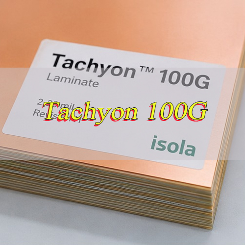
What Is Tachyon 100G?
Tachyon 100G is an Isola ultra-low-loss laminate and prepreg material for very high-speed digital PCB designs. It is intended for data rates of 100 Gb/s and beyond. The material is recognized under IPC-4103/17 and IPC-4101/102 and is RoHS compliant.
The standard laminate offering covers 2 to 20 mil, or 0.05 to 0.51 mm. Listed copper weights include 0.5 oz, 1 oz and 2 oz. Thinner and heavier copper foil can also be available.
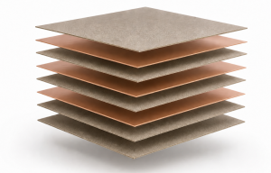
Unlike standard FR-4, this laminate system focuses on loss control and stable electrical behavior. Low Dk glass, square weave glass and mechanically spread glass are available. Low-profile copper options also help reduce conductor loss.
As a result, this high-speed PCB material is a strong fit for backplanes, daughter cards and line cards. It is most useful when insertion loss and timing margin directly affect channel performance.
Why Is Tachyon 100G Suitable for Ultra-Low-Loss High-Speed PCBs?
The material combines low dielectric loss, stable electrical properties and low-profile copper options. Its electrical behavior remains stable from -55°C to +125°C and at frequencies up to 100 GHz.
Its main advantages include:
- Low dielectric loss: A typical Df of 0.0021 limits dielectric loss as frequency rises.
- Stable Dk: A Dk of 3.02 at 5 GHz and 10 GHz supports predictable impedance design.
- Spread glass options: Spread glass helps reduce local dielectric variation and differential skew.
- Low-profile copper: HVLP3, HVLP and Advanced RTF options reduce roughness-related conductor loss.
- Low Z-axis expansion: A pre-Tg Z-axis CTE of 45 ppm/°C supports plated-hole reliability.
- Strong thermal capability: The material supports six 260°C reflow cycles and six 288°C solder-float exposures.
- HDI compatibility: Multiple lamination cycles and HDI processing are listed as material advantages.
In practice, these properties help improve eye opening and reduce jitter in loss-sensitive digital channels. They do not correct poor routing, plane splits or long via stubs. The PCB design must still protect the complete signal path.
What Is the Dielectric Constant of Tachyon 100G?
The typical dielectric constant is 3.04 at 2 GHz and 3.02 at both 5 GHz and 10 GHz. The datasheet also lists a typical Df of 0.0021 across the stated 2–10 GHz values.
| Frequency | Dk | Df |
|---|---|---|
| 2 GHz | 3.04 | 0.0021 |
| 5 GHz | 3.02 | 0.0021 |
| 10 GHz | 3.02 | 0.0021 |
These values support controlled-impedance design and high-speed channel modeling. However, 3.02 should not be used as one universal value for every dielectric layer.
Glass style, resin content and pressed dielectric thickness can change the effective dielectric behavior. The exact laminate and prepreg construction should be confirmed before final routing.
For production, calculate impedance from the released stackup. Then verify the finished PCB with impedance coupons and actual manufacturing geometry.
What Is the CTE Value of Tachyon 100G Material?
The Z-axis CTE is 45 ppm/°C below Tg and 250 ppm/°C above Tg. Total Z-axis expansion from 50°C to 260°C is 2.5%. The X/Y-axis CTE below Tg is 15 ppm/°C.
| Direction | Condition | CTE |
|---|---|---|
| Z-axis | Pre-Tg | 45 ppm/°C |
| Z-axis | Post-Tg | 250 ppm/°C |
| Z-axis | 50–260°C | 2.5% |
| X/Y-axis | Pre-Tg | 15 ppm/°C |
Z-axis expansion matters during lamination, reflow and thermal cycling. Excessive expansion increases stress around plated through holes and internal copper connections.
Tachyon 100G thermal performance is especially relevant to high-layer-count PCBs and fine-pitch BGA structures. Even so, CTE must be reviewed with board thickness, via aspect ratio and total thermal exposure.
A high-performance material cannot compensate for poor drilling or weak hole-wall plating. Material behavior and PCB process control must be evaluated together.
Isola Tachyon 100G Material Properties & Datasheet Overview
The June 23, 2026 Revision H datasheet lists Tg 215°C, Td 360°C, Dk 3.02 and Df 0.0021 as headline values. Revision H also corrects the Df test method and provides detailed thermal, electrical and mechanical data.
Thermal and Electrical Properties
| Property | Typical Value | Test Method |
|---|---|---|
| Tg, DSC | 215°C | IPC-TM-650 2.4.25C |
| Tg, DMA | 230°C | IPC-TM-650 2.4.24.4 |
| Tg, TMA | 210°C | IPC-TM-650 2.4.24C |
| Td, 5% Weight Loss | 360°C | IPC-TM-650 2.4.24.6 |
| T260 | >60 min | IPC-TM-650 2.4.24.1 |
| T288 | >60 min | IPC-TM-650 2.4.24.1 |
| T300 | >20 min | IPC-TM-650 2.4.24.1 |
| Z-CTE, Pre-Tg | 45 ppm/°C | IPC-TM-650 2.4.24C |
| Z-CTE, Post-Tg | 250 ppm/°C | IPC-TM-650 2.4.24C |
| Z Expansion, 50–260°C | 2.5% | IPC-TM-650 2.4.24C |
| X/Y CTE, Pre-Tg | 15 ppm/°C | IPC-TM-650 2.4.24C |
| Thermal Conductivity | 0.42 W/m·K | ASTM E1952 |
| Thermal Stress | Pass | IPC-TM-650 2.4.13.1 |
| Dk, 2 GHz | 3.04 | IPC-TM-650 2.5.5.5 |
| Dk, 5 GHz | 3.02 | IPC-TM-650 2.5.5.5 |
| Dk, 10 GHz | 3.02 | IPC-TM-650 2.5.5.5 |
| Df, 2–10 GHz | 0.0021 | Bereskin Stripline |
| Volume Resistivity | 1.33 × 10⁷ MΩ-cm | IPC-TM-650 2.5.17.1 |
| Surface Resistivity | 1.33 × 10⁵ MΩ | IPC-TM-650 2.5.17.1 |
| Dielectric Breakdown | 60 kV | IPC-TM-650 2.5.6B |
| Arc Resistance | 125 sec | IPC-TM-650 2.5.1B |
| Electric Strength | 60 kV/mm | IPC-TM-650 2.5.6.2A |
Mechanical and Safety Properties
| Property | Typical Value | Test Method |
|---|---|---|
| CTI | Class 3, 175–249 V | UL 746A / ASTM D3638 |
| Peel Strength | 0.79 N/mm | IPC-TM-650 2.4.8C |
| Peel Strength After Stress | 0.96 N/mm | IPC-TM-650 2.4.8.2A |
| Flexural Strength, Length | 303 MPa | IPC-TM-650 2.4.4B |
| Flexural Strength, Cross | 283 MPa | IPC-TM-650 2.4.4B |
| Tensile Strength, Length | 207 MPa | ASTM D3039 |
| Tensile Strength, Cross | 172 MPa | ASTM D3039 |
| Young’s Modulus, Length | 2,551 ksi | ASTM D790-15e2 |
| Young’s Modulus, Cross | 2,417 ksi | ASTM D790-15e2 |
| Taylor’s Modulus, Length | 2,264 ksi | ASTM D790-15e2 |
| Taylor’s Modulus, Cross | 2,197 ksi | ASTM D790-15e2 |
| Poisson’s Ratio, Length | 0.165 | ASTM D3039 |
| Poisson’s Ratio, Cross | 0.156 | ASTM D3039 |
| Moisture Absorption | 0.1% | IPC-TM-650 2.6.2.1A |
| Flammability | V-0 | UL 94 |
| RTI | 130°C | UL 746 |
The Tachyon 100G thermal conductivity is 0.42 W/m·K. This is a laminate value, not a complete PCB thermal solution.
Copper planes, thermal vias, component power density and airflow still control board-level heat transfer. The datasheet also lists 0.1% moisture absorption, UL 94 V-0 and an RTI of 130°C.
The combined data show strong electrical and thermal capability. They also support complex multilayer PCB structures and repeated thermal processing.
What Thickness Options Are Available for Tachyon 100G Prepreg?
The datasheet does not publish one fixed thickness range for Tachyon 100G prepreg. The listed 2 to 20 mil range applies to laminate, not prepreg.
Available prepreg fabric options include low Dk glass, square weave glass and mechanically spread glass. Final dielectric thickness depends on glass construction, resin content, ply count and lamination press-out.
Therefore, select the prepreg by finished dielectric spacing and target impedance. Confirm the actual construction before releasing the PCB stackup for production.
How Should a Tachyon 100G PCB Stackup Be Designed for High-Speed Signals?
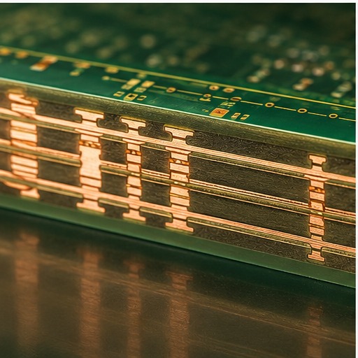
A Tachyon 100G PCB stackup should be built around channel loss, controlled impedance and continuous return paths. The material construction should be confirmed before final high-speed routing.
- Place high-speed signal layers beside continuous GND planes. SerDes and differential pairs require a stable return path. Avoid plane splits, large voids and reference changes beneath critical traces.
- Use the selected dielectric construction for impedance calculation. Do not apply Dk 3.02 to every layer without checking the actual buildup. Core, prepreg, glass construction and resin content can affect dielectric behavior.
- Control finished dielectric thickness. Trace width and spacing should be calculated from the pressed dielectric target. Prepreg nominal construction alone does not define the finished layer spacing.
- Use low-profile copper on loss-critical layers. HVLP3 is listed at ≤1.1 µm Rz JIS. HVLP and Advanced RTF are listed at ≤2.5 µm Rz JIS.
- Keep high-speed routes short and direct. Reduce unnecessary meanders and excessive layer transitions. Longer traces increase dielectric and conductor loss.
- Minimize signal via stubs. Review through-hole via length during channel simulation. Use back drilling when the remaining stub causes unacceptable resonance or return loss.
- Optimize anti-pad geometry. Via barrel, pad and anti-pad dimensions should be modeled together. Poor anti-pad design can create a large impedance discontinuity.
- Provide a return path at every layer transition. Place GND stitching vias close to signal vias. This gives return current a short path between reference planes.
- Control differential-pair geometry. Maintain the designed trace width, spacing and reference-plane distance. Avoid uncontrolled neck-down sections around BGA fanout and connectors.
- Review fiber-weave interaction. Spread-glass options help reduce local dielectric variation. Long differential pairs should still be reviewed for skew.
- Keep the layer buildup symmetrical. Balance dielectric thickness and copper distribution around the board centerline. This reduces bow, twist and lamination stress.
- Review copper distribution before lamination. Large copper-density differences can affect resin flow and pressed dielectric thickness. Copper balancing should be included in the manufacturing review.
- Plan BGA breakout before locking the stackup. Fine-pitch fanout can change via type, layer count and reference-plane continuity.
- Define controlled-impedance requirements in the fabrication data. Include target values, tolerances and trace layers. Suitable impedance coupons should be included for measurement.
- Verify the finished PCB. Impedance testing confirms the production geometry. Loss-sensitive projects may also require insertion-loss or channel-level validation.
The laminate, copper profile, via structure and return path must be designed as one high-speed channel. A Tachyon 100G PCB cannot deliver its expected performance with an uncontrolled stackup.
Tachyon 100G vs Megtron 6: Which Material Should You Choose?
For a numerical comparison, the exact MEGTRON 6 grade must be identified. The table below uses Panasonic MEGTRON 6 R-5775 as the comparison baseline.
| Property | Tachyon 100G | MEGTRON 6 R-5775 |
|---|---|---|
| Dk | 3.02 @ 10 GHz | 3.61 @ 10 GHz |
| Df | 0.0021 | 0.004 @ 10 GHz |
| Tg, DSC | 215°C | 185°C |
| Tg, DMA | 230°C | 210°C |
| Td | 360°C | 410°C |
| T288 | >60 min | >120 min |
| Z-CTE, Pre-Tg | 45 ppm/°C | 45 ppm/°C |
| Z-CTE, Post-Tg | 250 ppm/°C | 260 ppm/°C |
| X/Y CTE, Pre-Tg | 15 ppm/°C | 14–16 ppm/°C |
| Moisture Absorption | 0.1% | 0.14% |
| Peel Strength | 0.79 N/mm | 0.8 kN/m |
| Flammability | UL 94 V-0 | UL 94 V-0 |
Choose Tachyon 100G when dielectric loss and low nominal Dk are the main channel limits. Its published Df of 0.0021 is lower than the 0.004 value listed for R-5775 at 10 GHz.
MEGTRON 6 R-5775 shows stronger published Td and T288 values. It lists Td 410°C and T288 above 120 minutes. Tachyon 100G lists Td 360°C and T288 above 60 minutes.
For Z-axis expansion, the two materials are close. Both list 45 ppm/°C below Tg. The post-Tg values are 250 ppm/°C and 260 ppm/°C, respectively.
However, Dk and Df values should be reviewed with the test method and exact material construction. Published datasheet values support initial selection but do not replace channel simulation.
For long, loss-limited channels, Tachyon 100G has the stronger published dielectric-loss position. For an established MEGTRON 6 platform, qualification history and revalidation cost may justify retaining the approved material.
Where Is Tachyon 100G Commonly Used?
Tachyon 100G is mainly used where long channels and dense multilayer structures create signal-loss or thermal challenges. The material is common in networking, communications, computing, storage, aerospace and defense electronics.
Typical applications include:
- High-speed network backplanes
- Switch and router line cards
- Server PCB assemblies
- Data center hardware
- High-speed daughter cards
- Computing and storage systems
- High-layer-count communication PCBs
- Fine-pitch BGA PCB designs
- Aerospace electronic systems
- Defense communication electronics
A 100G interface does not automatically require this laminate. Channel length, connectors, via topology and copper roughness can change the loss budget.
For example, a short channel may have enough margin with another qualified low-loss material. A longer path with several transitions may benefit more from the ultra-low-loss dielectric system.
Select the material from the channel and reliability requirements, not from the product name alone.
What Affects Tachyon 100G PCB Cost?
Tachyon 100G PCB cost depends on material construction and manufacturing complexity. There is no fixed material or PCB price for every project.
The main cost factors include:
- Laminate construction: Core thickness and panel usage affect material cost.
- Prepreg selection: Glass construction, ply count and dielectric spacing change the multilayer buildup.
- Copper foil type: HVLP3, HVLP and Advanced RTF can change material sourcing.
- Copper weight: Standard listed options include 0.5 oz, 1 oz and 2 oz.
- Layer count: More layers increase laminate, prepreg, imaging and lamination work.
- Sequential lamination: Complex HDI structures add extra production stages.
- Drilling complexity: Small holes and thick boards increase drilling and plating control.
- Back drilling: Stub removal adds depth control and verification.
- Controlled impedance: Tight tolerances and coupon testing increase process control.
- Order quantity: Prototype and volume panel utilization are different.
The first cost-control step is to define the real channel-loss target. Do not use the highest-cost construction on every layer without a technical reason.
For procurement, lock the released stackup before requesting volume pricing. This makes PCB supplier quotations easier to compare and reduces later material changes.
Why Choose EBest Circuit as Your Tachyon-100G PCB Manufacturer?
Choosing the correct laminate is only the first step. EBest Circuit helps reduce stackup, material and production risks before volume manufacturing.
- Reduce stackup changes after layout release. We review laminate, prepreg, copper weight and dielectric spacing before production.
- Protect controlled-impedance performance. Trace layers, impedance targets and manufacturing geometry are reviewed together.
- Reduce material substitution risk. Specified laminate and copper-profile requirements can be identified before material release.
- Improve high-layer-count PCB manufacturability. Copper balance, drilling, lamination and board thickness are reviewed before production.
- Support loss-sensitive via structures. Back drilling, via stubs and high-aspect-ratio holes can be reviewed against the PCB structure.
- Maintain repeat-order consistency. Material and production information can be controlled for recurring and volume orders.
- Simplify PCB and PCBA sourcing. PCB fabrication, component sourcing, assembly and testing can be coordinated through one workflow.
- Match quality control to the project. AOI, electrical testing, impedance testing and microsection inspection can be applied as specified.
- Support regulated industry programs. EBest Circuit operates with ISO 9001, IATF 16949, ISO 13485 and AS9100D quality system capabilities.
- Buy directly from a China-based source manufacturer. Custom, prototype and volume PCB programs are manufactured in China and supplied worldwide.
The goal is to make your Tachyon 100G PCB stackup manufacturable, repeatable and ready for volume production.
FAQs About Tachyon 100G PCB Material
Q1: How should Tachyon 100G prepreg be stored before lamination?
A1: Store prepreg at 23°C or below and under 50% relative humidity. Keep it in the original packaging until use. FIFO inventory control also helps reduce moisture-related changes in resin flow and cure behavior.
Q2: Should opened Tachyon 100G prepreg be vacuum sealed?
A2: No. Remaining prepreg should be resealed with fresh desiccant and should not be vacuum sealed. Opened material should be used as soon as practical and protected from uncontrolled humidity.
Q3: What are the suggested starting lamination parameters?
A3: General starting parameters include 200°C cure temperature, 60 minutes at 200°C and a 3–5°C/min heat ramp. Product temperature should remain below 210°C. Final settings must match the actual multilayer construction.
Q4: Does a thick Tachyon 100G PCB require different drilling control?
A4: Yes. Boards above 2.5 mm with high layer counts may require a lower stack height and more conservative drilling parameters. Board thickness, copper structure and hole diameter should be reviewed before setting the drill program.
Q5: How many drill hits are recommended?
A5: A common processing guideline is a maximum of 1,000 hits for drills below 0.020 inch. Drills at or above 0.020 inch may reach 1,500 hits. Actual limits can be lower for thick or difficult PCB structures.
Q6: Does Tachyon 100G require plasma desmear?
A6: Not always. The material responds to chemical desmear. Plasma may help on thick or high-aspect-ratio PCBs where stronger hole-wall preparation is required before copper plating.
Q7: Is two-pass chemical desmear useful for thick boards?
A7: Two chemical-desmear passes may be considered for high-reliability PCBs or boards thicker than 2.5 mm. The exact process should be verified through hole-wall inspection and microsection analysis.
Q8: Can standard aqueous dry film be used for inner-layer imaging?
A8: Yes. Standard aqueous dry film can be used for inner-layer imaging. The material is also compatible with common cupric chloride and ammoniacal etching processes used in multilayer PCB fabrication.
Q9: Should panel flash be sheared after lamination?
A9: Routing is preferred instead of shearing. Removing panel flash by routing can reduce edge crazing risk after multilayer lamination and helps maintain cleaner panel edges before later fabrication processes.
Q10: Why is inner-layer dimensional movement important?
A10: Inner layers can change dimension after etching, oxide treatment and lamination. Artwork compensation should be based on measured production movement. Construction and grain orientation should remain controlled between repeat batches.
Q11: How should finished PCBs be packaged for long storage?
A11: Use a moisture barrier bag, humidity indicator card and suitable desiccant for long storage or high-temperature assembly programs. Finished PCBs should be dry before packaging.
Q12: How long should boards be used after opening the moisture barrier bag?
A12: A processing window of 168 hours is recommended when shop-floor conditions remain below 30°C and 60% RH. Bags opened only for inspection should be resealed promptly.
Tachyon 100G is built for PCB designs where channel loss, impedance stability and high-layer-count reliability directly affect product performance. The right laminate must be matched with the correct prepreg, copper profile, via structure and production stackup.
Do not wait until fabrication to discover that the released stackup is difficult to build or no longer meets the channel target. Send your Gerber or ODB++ files, stackup and impedance requirements to sales@bestpcbs.com. EBest Circuit will review your Tachyon 100G PCB project and provide a manufacturing quotation for prototype or volume production.