A micro circuit board compresses routing, components and interconnections into a tightly controlled footprint. Successful miniaturization depends on treating the board, component package, assembly process, enclosure and inspection plan as one system.
EBest supports PCB design, prototyping, fabrication, component sourcing, assembly and mass production. Start a compact-electronics project by submitting Gerber or ODB++, drill data, stackup targets, BOM, centroid data, assembly drawings and acceptance requirements for an engineering review.
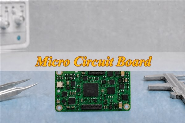
What Is a Micro Circuit Board and How Is It Different from a Mini or Standard PCB?
Density and process control define a micro circuit board. No universal board dimension defines the category. It usually combines a small outline with fine routing, compact packages, closely controlled registration and an assembly process designed for limited access.
| Board description | Typical design focus | Main manufacturing question |
| Standard PCB | Conventional component pitch and routing rules | Can normal drilling, imaging and assembly rules meet the design? |
| Mini PCB | Small mechanical outline | Does the reduced outline still use conventional features? |
| Micro PCB | Small outline plus dense interconnects and compact components | Which fine-feature, lamination, assembly and inspection controls are required? |
| Microchip circuit board | A colloquial term that may mean a tiny board carrying ICs | What actual board technology and package pitch does the product require? |
The label should therefore lead to a capability review, not a guessed rule set. A designer should specify the actual board outline, layer structure, component pitches, conductor geometry, via architecture and assembly constraints.
Where Are Micro Circuit Boards Used in High-Density and Compact Electronics?
Micro circuit boards fit more function into restricted spaces. The design must still protect serviceability and signal integrity. Typical applications include wearable sensors, compact diagnostic instruments, miniature cameras, hearing products, industrial sensing modules, robotics joints, aerospace instrumentation and portable communication devices.
- Medical electronics: compact sensing, data acquisition and wearable modules require documented materials, traceability and application-specific verification.
- Aerospace instruments: low mass and limited space must be balanced against vibration, thermal cycling and inspection access.
- Industrial sensors: dense analog, digital and power functions may share a small enclosure exposed to heat, moisture or electrical noise.
- Consumer and IoT products: antennas, batteries, connectors and user interfaces compete for the same mechanical envelope.
Application classification does not prove regulatory suitability. Medical, aerospace or safety-related projects require the product owner to define applicable standards, risk controls, validation evidence and change-control requirements.
How Small and Dense Can We Manufacture a Custom Micro Circuit Board?
No single dimension defines the manufacturable density limit. The real limit combines stackup, copper weight, via structure, laminate behavior, solder mask, component pitch and inspection method. A minimum trace or hole number alone cannot prove that the complete design is producible.
Before quoting a custom micro PCB design, EBest reviews the fabrication files and critical dimensions against the requested material, layer count and assembly plan. Exact line width, spacing, laser-via diameter, capture pad, annular ring, aspect ratio, finished thickness and tolerance must be confirmed for the individual build.
- Submit native constraints: identify controlled impedance, differential pairs, voltage spacing and current paths.
- Mark critical geometry: call out board edges, connector datums, keepouts, test points and component height limits.
- Separate prototype from volume assumptions: a laboratory build route may not provide the repeatability or throughput required for production.
- Request a stackup: route density should be checked against real dielectric and copper constructions before layout release.
What Design Requirements Should Be Considered for a Micro PCB?
Freeze fabrication and assembly rules before dense placement. The most expensive layout correction is often caused by choosing a package, via or connector that cannot be fabricated, assembled or inspected as planned.
- Freeze mechanical inputs: confirm the board outline, mounting points, flex zones, enclosure clearances and mating connector position.
- Define the stackup: assign reference planes, signal layers, power distribution and dielectric thicknesses before routing.
- Set package-aware rules: use land patterns, solder mask and paste apertures supported by component documentation and assembly review.
- Plan escape routing: evaluate fanout for fine-pitch BGAs, QFNs and compact connectors without violating return paths.
- Protect manufacturability: keep copper, holes and components clear of routed edges and scoring features by the approved amount.
- Design for inspection: preserve fiducials, probe access, polarity visibility and X-ray access where hidden joints are used.
- Control heat and power: verify copper area, thermal vias, temperature-sensitive parts and enclosure heat paths.
- Release one controlled dataset: align Gerber/ODB++, NC drill, netlist, BOM, centroid and drawings to the same revision.
How Do Fine Lines, HDI Microvias and Via-in-Pad Support PCB Miniaturization?
Fine lines and microvias release routing space. Via-in-pad also shortens layer transitions and frees escape channels around compact packages. These features can reduce board area, but each adds fabrication and reliability decisions.
An HDI PCB fabrication guide should be used to coordinate laser-via depth, capture pads, copper filling, sequential lamination and stackup symmetry. Via-in-pad beneath solderable lands normally requires a specified filling and planarization process so solder is not drawn into an open hole.
| Miniaturization feature | Design benefit | Control required |
| Fine lines and spaces | More routing channels within a smaller area | Copper thickness, imaging, etching and impedance review |
| Blind microvias | Short transitions between adjacent layers | Via depth, target pad, plating and registration control |
| Staggered microvias | Dense routing with reduced stacked-interface risk | Stackup and sequential-lamination planning |
| Stacked microvias | Vertical connection through multiple build-up layers | Structure-specific reliability evidence and process approval |
| Filled via-in-pad | Direct BGA escape and usable solder land | Fill quality, planarization, plating and assembly inspection |
Stacked structures should not be selected by routing convenience alone. Thermal excursions can expose weak microvia interfaces, so the approved structure and verification plan must match the product environment.
What Materials, Thicknesses and Stackups Are Suitable for Micro PCBs?
Application requirements determine material and thickness. Electrical, thermal, mechanical and assembly needs matter more than the word “micro.” Standard FR-4 may suit many compact products, while high-speed, flexible, rigid-flex or ceramic constructions address specific needs.
| Construction | Useful when | Confirm before release |
| Thin rigid FR-4 | The board must fit a shallow enclosure | Handling, bow and twist, copper balance and panel support |
| HDI multilayer | Fine-pitch devices require dense escape routing | Microvia sequence, lamination count, impedance and reliability |
| Flexible circuit | The circuit must fold, bend or replace wiring | Bend region, copper type, coverlay, stiffener and connector transition |
| Rigid-flex | Rigid component zones must connect through integrated flex regions | Transition design, layer mapping, bend control and assembly fixtures |
| Ceramic substrate | Thermal, dimensional or high-frequency needs justify a different material system | Metallization, assembly compatibility, brittleness and supplier process |
The standard thickness of a micro PCB is not a single value. An Extra Thin PCB requires project-specific confirmation of finished thickness tolerance, copper distribution, panel handling and assembly support.
How Are Micro Circuit Boards Manufactured?
Micro PCB fabrication requires tighter process coordination. It follows the standard multilayer sequence but applies closer control to imaging, lamination, drilling, plating and inspection. The process must follow the approved stackup and via architecture.
- CAM and DFM review: verify layer data, drills, netlist, stackup, panel strategy, coupons and critical dimensions.
- Inner-layer preparation: clean copper-clad cores and apply photoresist under controlled conditions.
- Laser imaging and development: transfer dense conductor patterns with registration appropriate to the construction.
- Etching and inner-layer AOI: form conductors and compare them with the design data before lamination.
- Oxide treatment and layup: prepare bonding surfaces and align cores, prepregs and copper foils.
- Lamination: consolidate the stack under a controlled heat and pressure cycle.
- Mechanical or laser drilling: create through holes, blind vias or microvias according to the build sequence.
- Desmear and metallization: condition hole walls, deposit conductive seed layers and plate copper.
- Sequential build-up: repeat imaging, lamination and laser drilling when the HDI structure requires additional layers.
- Outer-layer imaging and plating: form external conductors and plated features.
- Solder mask and surface finish: define solderable areas and protect exposed copper using the approved finish.
- Profiling and electrical test: route or laser-cut the outline, test connectivity and verify required dimensions.
- Final inspection: review workmanship, documentation, coupons and order-specific acceptance evidence.
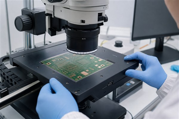
How Are Micro Printed Circuit Boards Assembled?
Printing, placement and reflow stability control assembly quality. Inspection must also detect hidden or closely spaced joints. Hand soldering may support limited rework, but it cannot replace a validated fine-pitch production process.
- Assembly DFM: review land patterns, spacing, polarity, fiducials, panel rails, tooling access and component heights.
- Material control: confirm component identity, moisture sensitivity, storage and traceability requirements.
- Stencil preparation: match foil thickness and aperture design to the smallest and largest solder deposits on the board.
- Solder paste inspection: detect insufficient, excessive, shifted or bridged deposits before placement.
- Precision placement: use suitable feeders, vision alignment and board support for compact components.
- Reflow: develop a profile compatible with the paste, package mass, board construction and component limits.
- Inspection and rework: combine AOI, X-ray where hidden joints require it, electrical checks and controlled rework instructions.
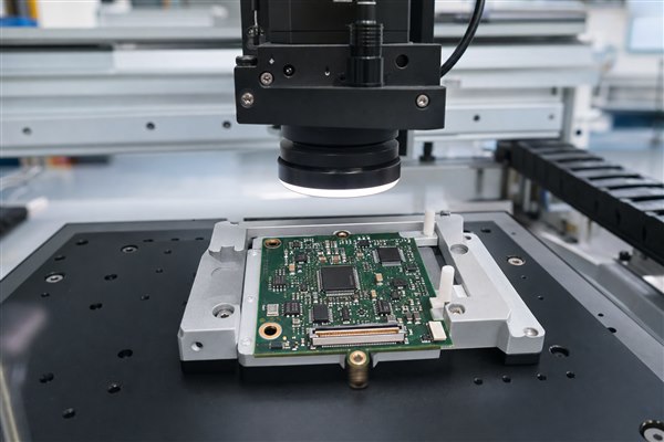
What Testing Is Required for Micro Circuit Boards and Assemblies?
Visual inspection alone cannot release a dense assembly. Testing must prove connectivity, workmanship and application-specific function. Dense boards reduce probe access and may hide solder joints, so the test strategy should be defined before layout is frozen.
| Quality gate | Risk controlled | Evidence to request |
| Inner- and outer-layer AOI | Opens, shorts and conductor anomalies | Inspection disposition tied to the production lot |
| Electrical test | Net continuity and isolation failures | Test completion record and approved netlist basis |
| Microsection or coupon review | Hole, plating and layer-registration concerns | Order-specific coupon or section results when required |
| SPI and AOI | Paste and visible assembly defects | Inspection criteria and defect disposition |
| X-ray inspection | Hidden BGA, QFN or filled-via joint concerns | Images or inspection record for agreed locations |
| ICT, flying probe or functional test | Electrical and product-level failures | Approved test limits, procedure and result format |
What Custom Micro PCB Prototyping, Manufacturing and Assembly Services Can We Provide?
EBest supports the complete compact-board production path. Services include PCB design, prototyping, component sourcing, fabrication, assembly and mass production. One project path keeps layout constraints, board construction, component availability and assembly access aligned to the same revision.
- PCB design support: review the board outline, stackup, fine-pitch fanout, power distribution, connector position and test access before manufacturing files are released.
- Prototype production: build samples to verify mechanical fit, component orientation, solderability, electrical behavior and assembly access before committing to a larger order.
- Custom board fabrication: evaluate standard FR-4, multilayer, HDI, extra-thin, flexible, rigid-flex, high-frequency, high-Tg, ceramic, metal-core and impedance-controlled constructions against the application.
- Component sourcing: check manufacturer part numbers, package compatibility, lifecycle status and approved alternatives so BOM changes do not reach the assembly line without review.
- PCB assembly: coordinate stencil data, placement files, polarity, reflow, visible-joint inspection, hidden-joint inspection and the agreed electrical or functional test scope.
- Mass-production transfer: carry the approved stackup, material set, BOM revision and acceptance criteria from prototype into repeat production, reducing avoidable requalification work.
- Quality and schedule planning: match the supplied ISO 9001, ISO 13485, IATF 16949, AS9100D, UL, RoHS and REACH information to contractual needs. EBest’s stated expedited service, including possible shipment within 24 hours, remains subject to material, design, capacity and test feasibility.
Send the actual fabrication and assembly package for confirmation of line width, spacing, via construction, finished thickness, package handling, inspection access and production schedule. A generic capability label cannot replace a design-specific review.
Custom Medical Micro Circuit Board Manufacturing and Assembly Case Study
Controlled inputs make a medical micro PCB case credible. This representative case follows a compact sensing board from mechanical constraints to verifiable assembly evidence.
Project Background: A portable monitoring module needed to fit signal acquisition, processing, power regulation and a board-to-board connector inside a shallow enclosure. The connector datum, mounting holes and component-height envelope could not move after the enclosure tooling was approved.
Project Requirements: The release package contained Gerber/ODB++, NC drill, a target stackup, BOM, centroid data, assembly drawings and the enclosure model. It also defined approved component manufacturers, polarity references, cleanliness limits, traceability fields, test-point nets and electrical acceptance limits.
Our Solution — Design Review: The engineering review checked whether the selected packages could escape without breaking reference planes, then aligned the via structure with an available stackup. Connector pads and mounting holes were checked against mechanical datums. Sensitive analog routing was separated from switching power paths.
Our Solution — Production Controls: Component spacing was reviewed for stencil release, placement nozzles, optical access and controlled rework. Hidden joints requiring X-ray were identified before assembly. The team returned one consolidated question list before tooling and applied the traceability logic used for high reliability medical PCBA planning to BOM, material and revision control.
Output Results: The defined outputs included an approved fabrication and assembly dataset, controlled prototype boards and assembled samples. Agreed inspection records, electrical test results and a signed revision baseline gave the customer verifiable evidence for device-level validation without claiming regulatory approval or field performance.
What Affects Micro PCB Prototype Cost and Production Lead Time?
Extra process cycles increase cost and lead time. Specialized materials, tighter controls and difficult component handling add further pressure. Quotes are comparable only when suppliers use the same data revision and acceptance scope.
- HDI build sequence: sequential lamination, stacked or filled microvias and via-in-pad add process steps and verification.
- Material availability: uncommon laminate, copper or thickness combinations can extend preparation time.
- Panel utilization: a tiny board is not automatically inexpensive if tooling rails, coupons or irregular outlines reduce usable panel area.
- Assembly density: small packages, mixed component sizes, X-ray needs and controlled rework affect setup and inspection.
- Test scope: fixtures, programming, functional simulation and documentation require approved procedures and inputs.
- Revision stability: late BOM, stackup or mechanical changes reset engineering work and may invalidate prepared tooling.
EBest states that expedited service may be available, including urgent shipment within 24 hours for feasible orders. That statement must not be treated as a promise for a micro PCB until material, design, capacity, assembly and test scope are reviewed in writing.
Why Choose EBest Circuit as Your Micro Circuit Board Manufacturer?
One coordinated supplier reduces handoff risk. EBest connects design, prototyping, fabrication, sourcing, assembly and mass-production support for compact-board projects. Each advantage below links the service to a practical customer benefit.
- Fewer responsibility gaps: one project path connects layout, bare-board fabrication, sourcing and assembly, reducing disputes when a footprint, material or component change affects more than one supplier.
- Lower respin risk: fabrication and assembly constraints are reviewed before tooling, helping expose impossible fanout, inaccessible test points, connector interference and stencil conflicts while they are still editable.
- Better construction fit: EBest’s supplied range includes FR-4, multilayer, HDI, extra-thin, flexible, rigid-flex, high-frequency, high-Tg, ceramic and metal-core boards. Customers can compare constructions against size, bending, thermal and signal requirements instead of forcing every design onto standard FR-4.
- More controlled BOM changes: component sourcing is connected to package, lifecycle and approved-alternative review, reducing the risk that an available substitute creates a new footprint or assembly problem.
- Smoother production transfer: prototype stackup, material, BOM and acceptance decisions can become the repeat-order baseline, reducing duplicated engineering work and uncontrolled revision drift.
- Clearer release evidence: quality-system information and order-specific inspection or test records can be matched to the customer’s contract before production, preventing certificate names from being mistaken for actual acceptance evidence.
- Feasible urgent planning: EBest states that expedited shipment may be available for urgent boards. Confirming files, materials, capacity, assembly and test scope first gives customers a usable commitment instead of an unsupported speed promise.
Send the complete project package instead of only a board image or dimensions. EBest can then review the micro circuit board against real construction, sourcing, assembly and acceptance requirements before confirming the quotation.
FAQs About Micro Circuit Boards
Q1: How should ultra-small micro circuit boards be panelized?
A1: Stable handling is the priority. Confirm rail width, tooling holes, fiducials, breakaway tabs, component clearance and the depanelization method with both the fabricator and assembler.
Q2: Which surface finish is suitable for fine-pitch micro PCB pads?
A2: Planarity and solderability govern the choice. Compare finish thickness, shelf life, wire-bonding needs, assembly cycles and service conditions before selecting ENIG, ENEPIG, immersion silver, immersion tin or another approved option.
Q3: How can tombstoning be reduced on a densely populated micro PCB?
A3: Balance the wetting forces. Check land-pattern symmetry, copper connections, paste deposits, stencil apertures, placement accuracy and the reflow profile when small passive components repeatedly stand on one end.
Q4: When should moisture-sensitive components be baked before assembly?
A4: Follow the component moisture limits. Baking depends on moisture sensitivity level, packaging condition and floor-life exposure. Use the supplier’s handling requirements and the agreed assembly procedure rather than applying one bake cycle to every device.
Q5: Should solder mask openings be shared between fine-pitch pads?
A5: Use manufacturable mask geometry. Shared openings may be necessary when individual mask dams cannot be produced reliably or the land pattern requires them. The final rule must reflect achievable mask registration and bridge width.
Q6: How should flux residue and cleanliness be specified?
A6: Specify measurable cleanliness requirements. Base them on the product environment, flux system and acceptance criteria. Define prohibited residues, ionic-cleanliness evidence, coating compatibility and component restrictions instead of requesting cleaning by habit.
Q7: How can a micro PCB be depanelized without damaging nearby components?
A7: Control stress during separation. Keep fragile parts away from break lines. The panel drawing should define tab positions, scoring or routing, allowable edge stress, board support and the tool used to prevent bending.
Q8: How should alternative components be approved for repeat production?
A8: Approve every substitute before production. Review manufacturer part number, package, electrical rating, lifecycle and assembly impact. Also verify footprint, polarity, height, thermal behavior and test consequences.
Q9: What traceability records are useful for repeat micro PCB orders?
A9: Link each shipment to approved inputs. Useful records include revision, material lot, component lot or date code, production batch, inspection disposition, test result and approved deviation history.
Q10: How should assembled micro circuit boards be packaged for shipment?
A10: Protect against ESD, moisture and impact. Packaging must not load small components or connectors. Define antistatic protection, tray or carrier support, desiccant, humidity indication, quantity per pack and orientation before shipment.
Conclusion
Reliable micro PCBs require one controlled production system. Review the stackup, fine-pitch packages, via structure, materials, component supply, assembly process and acceptance evidence together. Resolving these constraints before tooling reduces respins, substitutions, assembly defects and unclear release decisions.
Send EBest your Gerber/ODB++ and NC drill, stackup, BOM and quantities, plus assembly, programming and test requirements. Email sales@bestpcbs.com to confirm manufacturability, prototype and mass-production options, delivery feasibility and a formal quotation.