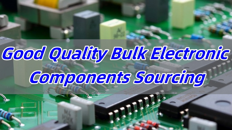
Bulk electronic components sourcing can be a turning point in project success, especially when production scales up. Whether you’re managing a tight schedule or handling complex BOMs, finding a reliable supply chain is critical to avoid disruptions, cost overruns, or inventory pileups.
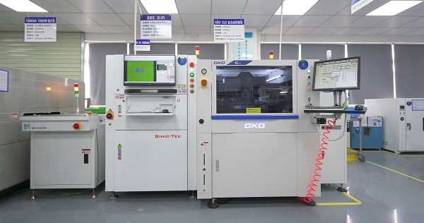
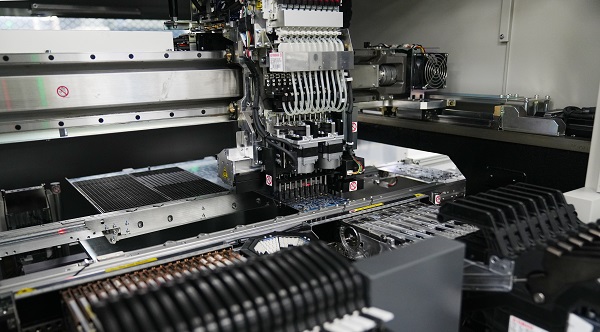
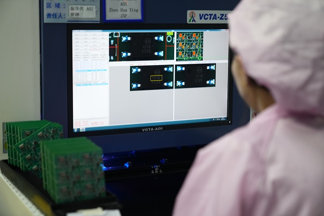
EBest Circuit (Best Technology) provides good quality bulk electronic components sourcing to a fiercely competitive market. As a major manufacturer of PCB and PCBA, we have integrated hundreds of bulk electronic components suppliers, and electronic product brands. We have a full supply chain, and we can get the material price fluctuation information and adjust our procurement strategies accordingly. We have advanced inspection equipment like AOI, X-ray. And all the processes from material sourcing to final box assembly comply with the rigorous standards, such as ISO 9001, ISO 13485, IATF 16949, AS9100D, UL, REACH, RoHS. For any bulk electronic components sourcing needs, or any EMS PCB manufacturing projects that need us to help, pls shoot us an email at sales@bestpcbs.com.
What Is Bulk Electronic Components?
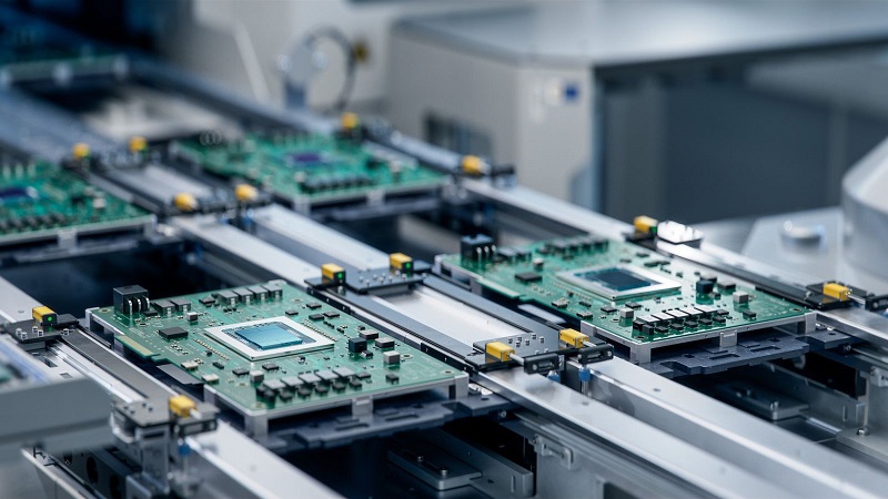
Bulk electronic components refer to large-quantity purchases of resistors, capacitors, ICs, connectors, or other passive and active devices used in circuit boards. These parts are typically packed in reels, trays, or bags and shipped in lots to meet production demands. Buying in bulk helps reduce per-unit costs, simplifies logistics, and supports faster manufacturing cycles.
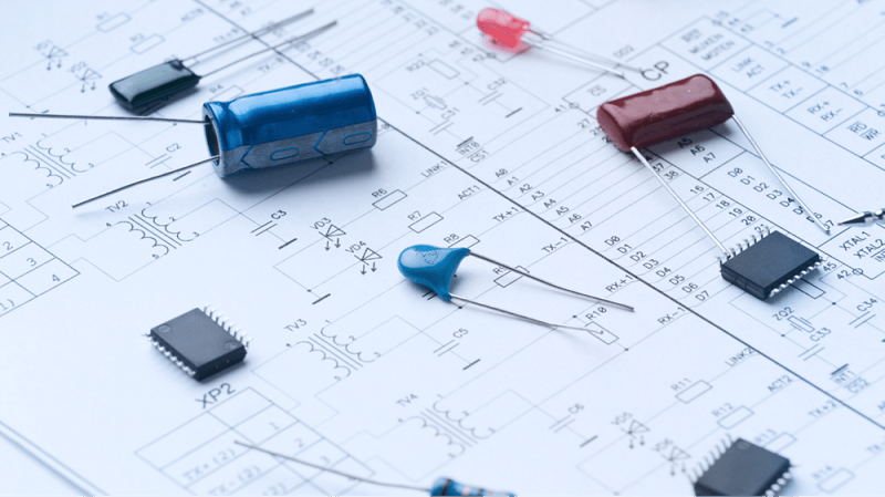
What Are the Basic Electronic Components?
Before sourcing, understanding the basics is helpful. The core components include:
Resistors: Control voltage and current in circuits.
Capacitors: Store and release electrical energy.
Diodes: Allow current to flow in one direction only.
Transistors: Amplify or switch electronic signals.
Integrated Circuits (ICs): Miniaturized circuits in a chip form.
Connectors: Link circuit boards to other components or power.
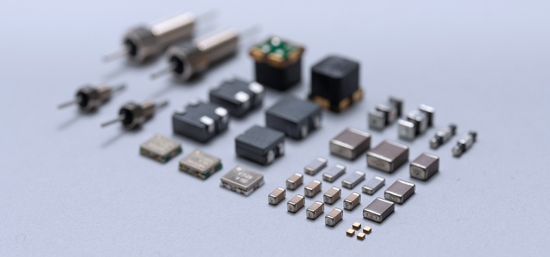
What Are Types of Electronic Components Packages?
Electronic components are available in various packages to fit design needs. The most common types are:
Through-Hole: Leads go through the board, used for mechanical strength.
Surface Mount (SMD): Smaller, mounted directly onto the board’s surface.
Ball Grid Array (BGA): Used for high-density ICs, such as processors.
Chip-on-Board (COB): ICs mounted directly onto the board substrate.
What Are Bulk Electronic Components Suppliers?
Bulk suppliers offer large volumes of components to OEMs, EMS providers, and manufacturers. Their inventory must be extensive, with short lead times. A supplier should provide traceable parts, full certifications, and test reports to ensure quality.
EBest Circuit (Best Technology) stands out by combining all these qualities. We use MES systems to ensure traceability and quality tracking. Our partnerships with global distributors reduce sourcing risks, while our on-site engineers help verify component authenticity.
Who Are Wholesale Electronic Components Shops in Johannesburg?
Johannesburg has a growing electronics market. Shops like RS Components South Africa, Mantech Electronics, and Communica are known suppliers. However, local stock may be limited during peak cycles. For large-volume PCB & PCBA orders, professional sourcing partners like EBest Circuit (Best Technology) provide a broader selection and professional bulk electronic components support.
How to Find Reliable Bulk Electronic Components Online?
To avoid counterfeit parts and long wait times, consider the following steps:
Verify the source: Choose distributors with ISO certifications and traceable supply chains.
Check technical specs: Always confirm datasheets, lot numbers, and RoHS compliance.
Read reviews: User feedback helps identify supplier strengths and gaps.
Ask for samples: Test small batches before scaling up to full orders.
Review warranty and return policies: Ensure risk-free buying terms.
With EBest Circuit (Best Technology), we not only vet suppliers but also apply rigorous quality checks before shipping. That helps reduce failures by up to 30% compared to market averages.
Where to Buy Bulk Electronic Components in China?
Shenzhen and Dongguan are key sourcing hubs in China. Platforms like Huaqiangbei, LCSC, and DigiKey China provide a wide range. But navigating language, logistics, and MOQ terms can be tough.
Our team at EBest Circuit (Best Technology) bridges this gap. We handle language barriers, inspect goods on-site, and negotiate MOQ terms. As a PCB and PCBA manufacturer, we offer bundled sourcing, assembly, and testing to shorten the supply chain and improve reliability.
Why Choose EBest Circuit (Best Technology)?
Here’s why our clients trust us when it comes to sourcing bulk electronic components:
Stable supply: Our distributed sourcing model shields against regional disruptions.
Component tracking: Each batch has full traceability through MES and blockchain solutions.
Custom sourcing: We help customers with rare or obsolete components through global distributor networks.
Quality assurance: All parts undergo AI-driven optical inspections and X-ray analysis when needed.
Flexible MOQs: We help startups and small manufacturers by breaking large MOQs into manageable volumes.
Fast Tech Updates: Our BOM engineers regularly check part lifecycle status, so your product won’t be based on obsolete components.
Efficient Procurement: EBest Circuit (Best Technology) offers one-stop BOM kitting. No more chasing 10 suppliers and waiting for 5 quote rounds.
To wrap up, choosing the right supplier for bulk electronic components is not just about price. It’s about delivery assurance, inventory control, and long-term support. With EBest Circuit (Best Technology), you gain a supply partner who understands every detail—from procurement strategy to viable PCBA solution. Welcome to follow us on YouTube or shoot us an email at sales@bestpcbs.com. We are glad to provide the specific quote and the corresponding solution based on your particular project needs.
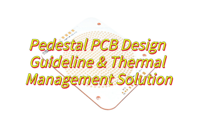
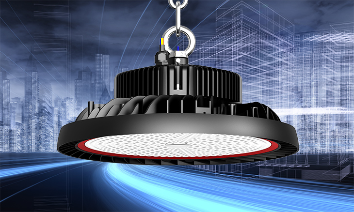
Looking for pedestal PCBthermal management solution? This guide covers design, specifications, functions, and thermal solutions for optimal performance.
Are you still worried about heat dissipation?
Does high temperature cause a sharp decrease in device life?
Does the heat sink take up valuable layout space?
Does thermal cycling cause solder joint failure?
EBest Circuit (Best Technology) Can Provide Solution:
Copper pillar direct connection technology – 60% reduction in thermal resistance.
Intelligent thermal distribution design – 45% improvement in temperature uniformity.
Material optimization solution – Eliminate thermal stress damage.
Welcome to contact us if you have any request for pedestal PCB design and manufacturing: sales@bestpcbs.com.
What Is A Pedestal PCB?
Apedestal PCB features built-in conductive pillars made of copper or aluminum that elevate components above the main circuit board. These pillars serve multiple functions: they transfer heat from high-power components to cooling systems, reducing operating temperatures by 20-35°C; they strengthen the board’s structure to prevent solder joint failures in high-vibration environments; and they provide electromagnetic shielding to protect sensitive signals.
Manufactured with precision laser drilling, the pillars maintain tight height tolerances within ±0.05mm. This technology is particularly valuable in 5G networks, automotive radar, and industrial equipment where thermal management, durability, and signal clarity are crucial.
The design combines thermal performance with mechanical stability while maintaining electrical connections through conductive vias, making it ideal for demanding electronic applications.
Copper foil expansion: 3x component size under heat sources
Thermal separation structure reduces thermal resistance by 40%
Electrical
Dielectric strength: ≥3kV (industrial)
Min. conductor spacing: 0.2mm
Impedance control: ±10% tolerance
Manufacturing
Thickness tolerance: ±0.1mm (FR-4)
CNC drilling accuracy: ±25μm
Copper adhesion: ≥0.8N/mm²
Environment
Operating temp: -40°C to +150°C
Halogen-free materials (RoHS 3.0 compliant)
Documentation
Must include: Component layout, impedance values, thermal resistance parameters
What Are Functions of Pedestal PCBs?
Mechanical Fixation
Serves as a rigid carrier to precisely secure components (e.g., IC chips, connectors), preventing vibration-induced solder joint fractures or displacement (e.g., ensuring reliability in industrial controllers under vibratory conditions).
Electrical Interconnection
Enables signal transmission and power distribution between components via copper traces and vias, supporting high-speed signals (e.g., PCIe interfaces) or high-current applications (e.g., motor drivers).
Thermal Optimization
Integrates copper planes/thermal via arrays to direct heat away from high-power components (e.g., metal-core PCBs for LED driver boards).
Power Distribution Network (PDN)
Designs dedicated power layers or wide traces to reduce impedance and stabilize voltage supply (e.g., multi-phase power designs in server motherboards for CPU dynamic frequency scaling).
Signal Integrity (SI) Assurance
Controls impedance and adds shielding layers to suppress EMI, ensuring distortion-free transmission of high-speed signals (e.g., DDR4/5 memory buses).
Modular Expansion
Provides standardized interfaces (e.g., edge connectors, board-to-board connectors) for plug-and-play integration of functional subcards (e.g., 5G modules) or RF assemblies.
What Are Applications of Pedestal PCB?
LED Lighting: High-brightness LED bulbs for thermal management
Automotive Electronics: EV battery systems and motor controllers
Industrial Automation: PLCs and robotics for stable operation
Medical Instruments: Imaging devices like X-ray machines and CT scanners
Telecommunications: Routers, base stations, and RF amplifiers
Consumer Devices: TVs, cameras, and audio equipment
Computing Hardware: Motherboards and expansion cards in servers
Looking for reliable circuit board assembly services? At EBest Circuit (Best Technology), we provide full-service PCB assembly solutions that include SMT, through-hole, mixed assembly, and turnkey capabilities. Whether you’re building prototypes or going into mass production, we support your project from start to finish with engineering guidance, quality control, and fast lead times.
What Are Circuit Board Assembly Services?
Circuit board assembly services play a crucial role in the electronics manufacturing industry. They involve the process of placing electronic components onto a blank PCB to form a functioning circuit. This process transforms a bare board into a working device. It’s used in every industry that depends on electronics — from smartphones and cars to medical devices and aerospace equipment.
There are three main methods in circuit board assembly:
SMT (Surface Mount Technology): Components are mounted directly onto the surface of the PCB.
THT (Through-Hole Technology): Leads are inserted into holes in the PCB and soldered underneath.
Mixed Assembly: Combines both SMT and THT for boards that require diverse components.
Understanding these methods helps new customers communicate better with suppliers and choose the right assembly process based on the design and function of their product.
Types of Circuit Board Assembly Methods
Different circuit designs and application needs call for different assembly methods. Here’s a breakdown:
Surface Mount Technology (SMT)
SMT is the most common technique in use today. Components are placed directly on the PCB surface, enabling smaller designs, higher component density, and faster assembly. Automated pick-and-place machines position these components with high precision. It’s suitable for compact and high-speed devices such as smartphones, tablets, and IoT products.
Through-Hole Technology (THT)
THT involves placing components with wire leads through pre-drilled holes in the PCB. The leads are soldered on the opposite side. This method offers greater mechanical strength and is often used for components that experience physical stress or need a strong bond, like connectors or transformers. THT is common in industrial and automotive PCBs.
Mixed Assembly
When a PCB requires both surface-mounted components and through-hole parts, a mixed assembly approach is used. It’s often found in complex designs, especially when different voltage levels or mechanical supports are needed. Mixed assembly offers more flexibility but also requires advanced equipment and careful coordination.
Dual In-line Package (DIP) Assembly
DIP is a specific type of through-hole assembly method that uses components with two parallel rows of pins (leads). These components are inserted into matching holes on the PCB and are often hand-soldered or wave-soldered. DIP is commonly used for ICs (integrated circuits), microcontrollers, and programmable logic devices during development or low-volume production. While not as compact as SMT, DIP is easier to prototype and replace, making it useful in educational, industrial, and repair applications.
Turnkey vs. Consigned PCB Assembly: What’s the Difference?
When working with an assembly partner, it’s essential to choose the right sourcing model:
1. Turnkey Assembly
In a full-turnkey model, the assembly provider takes care of everything. This includes sourcing components, manufacturing the PCB, assembling parts, testing, and delivery. It’s a hands-off approach for the customer and is preferred by startups or teams with limited resources. It reduces management complexity and lead times.
2. Consigned Assembly
With consigned assembly, the customer provides some or all the components. This is ideal for companies that already have components in stock or require tight control over part sourcing. While it offers flexibility, it also requires more effort from the client to ensure timely material delivery.
3. Partial Turnkey
A hybrid of the two, partial turnkey services split responsibilities — the customer supplies some components, and the assembler handles the rest. This balances control and convenience.
At EBest Circuit (Best Technology), we offer both full turnkey PCB assembly service and consigned assembly. All of our components are sourced from authorized distributor or digikey, mousers, find chips and so on. We have established stable bussiness relationship with them, so that we can get the best price and shorter lead time.
Key Capabilities of Our Circuit Board Assembly Services
At EBest Circuit (Best Technology), we bring years of experience and investment in equipment to deliver top-quality PCB assembly services.
1. SMT Line Capability
We operate 4+ advanced SMT production lines capable of handling fine-pitch, small components (as small as 01005) both in China and Vietnam. Each line supports:
Single- and double-sided placement
Reflow soldering with nitrogen ovens
Automatic solder paste printing with SPI (Solder Paste Inspection)
High-Speed Pick and Place
Dual online AOI
X-ray inspect machine for fine pitch BGAs
Our pick-and-place machines operate at speeds up to 80,000 components per hour, providing high efficiency for volume production. These machines offer accurate placement and are suitable for dense and complex boards.
2. Fine-Pitch and BGA Soldering
We’re capable of mounting fine-pitch ICs, BGA, QFN, and other challenging components. Our BGA rework station ensures precise alignment and reliable solder joints — ideal for high-reliability sectors like aerospace and medical.
3. Leaded and Lead-Free Options
We offer both leaded and lead-free soldering, depending on your application and regulatory requirements. All lead-free processes are compliant with RoHS and REACH directives.
4. Component Sourcing and BOM Management Support
Managing the bill of materials (BOM) is one of the most complex parts of circuit board assembly. We simplify this process:
Global Sourcing Network: We work with trusted distributors like Digi-Key, Mouser, Arrow, and Avnet.
Alternate Part Suggestion: If parts are obsolete or out of stock, our engineers will recommend alternatives based on functionality and compatibility.
Cost Control: We offer multiple supplier options and volume purchasing strategies to help reduce costs.
Inventory Tracking: Our MES system ensures full traceability from incoming materials to final product.
DFM & DFA checks before assembly with free services
5. Various PCB Assembly Support
We support various PCB assembly, including:
Rigid FR4 PCB
Metal core PCB
Ceramic PCB
Rigid flex PCB
Flex circuits
FR4 PCB with metal dome assembly
Box building assembly
Whether your project is a prototype or a large batch, we’ll handle procurement smoothly to keep things on schedule.
PCB Testing and Quality Inspection Services
Quality is not just a checkbox — it’s a process. Our multi-stage inspection services help identify issues early and deliver reliable products.
AOI (Automated Optical Inspection)
AOI checks for soldering defects, missing components, and polarity errors. It’s especially useful for SMT lines and runs on every board before moving to the next step.
X-ray Inspection
We use X-ray machines to inspect solder joints under BGAs and other invisible parts. This non-destructive method ensures hidden connections are properly made.
ICT and Functional Testing
We support In-Circuit Testing (ICT) and Functional Testing (FCT) using customer-provided test fixtures or our internal jigs. This verifies each component’s performance and the overall function of the board.
Visual Inspection (IPC-A-610)
Our trained QC staff visually inspects boards under IPC-A-610 standards, covering cosmetic and dimensional defects.
Certifications and Quality Standards We Follow
We understand the importance of compliance. That’s why EBest Circuit (Best Technology) adheres to the following certifications and standards:
ISO9001: General quality management system for manufacturing.
ISO13485: Standard for medical device assembly.
IATF16949: Automotive-grade quality system for reliability and traceability.
UL Certification: For products entering North American markets.
RoHS and REACH: Compliance with hazardous substance control.
IPC-A-610: Acceptance standards for electronic assemblies.
These certifications reflect our commitment to consistent quality and customer satisfaction.
Fast Prototyping and Quick-Turn Assembly Options
Startups, design houses, and R&D teams often need fast iterations. We support quick-turn prototypes with lead times as fast as 24–72 hours, depending on complexity and material availability.
No MOQ for prototypes.
DFM (Design for Manufacturability) checks to avoid errors.
Engineering support to adjust layout and improve yield.
For urgent projects, we offer expedited services at competitive rates. Speed doesn’t mean sacrificing quality — our rapid builds go through the same rigorous inspection process.
Industries We Serve with PCB Assembly Services
Our experience spans multiple industries, each with unique demands:
Consumer Electronics: Wearables, smart devices, gaming consoles, and home automation.
Automotive: In-vehicle infotainment, power control modules, and driver-assist systems.
Medical Devices: Heart rate monitors, wearable health trackers, and diagnostic equipment.
Industrial Automation: Sensor boards, motor controllers, and factory equipment.
Aerospace & Military: Avionics modules, communication devices, and tactical systems.
Our engineering team understands the compliance, testing, and documentation needs of each industry, making us a trusted partner.
Why Choose Us for Your Circuit Board Assembly Needs?
At EBest Circuit (Best Technology), we’re not just a PCB manufacturer — we’re a complete solution provider.
One-Stop Manufacturing: From PCB fabrication and component sourcing to final assembly and testing.
Engineering Support: Our team helps you optimize your design for performance and manufacturability.
Strict Quality Control: We apply multiple checkpoints to ensure every product meets expectations.
Competitive Pricing: We balance cost, quality, and speed through strategic sourcing and lean manufacturing.
Global Delivery: Our logistics team ships to over 80 countries with fast turnaround times.
Our approach combines reliability, speed, and technical depth — all under one roof.
How to Get a Quote for Circuit Board Assembly Services?
We make it easy for you to start working with us. Here’s how the quote process works:
Upload Your Files: Submit your BOM, Gerber files, and assembly drawings via our website or email.
Engineering Review: Our team will review the files and provide DFM feedback if needed.
Get a Quotation: You’ll receive a detailed quote within 24–48 hours.
Sample Production: Once approved, we make a prototype or pre-production sample for confirmation.
Mass Production: After sample approval, full production begins with agreed lead times.
We’re happy to guide you through the process — whether you’re an experienced engineer or a first-time product developer.
FAQs About Circuit Board Assembly
1. What files do I need to provide for PCB assembly?
You should provide Gerber files, BOM (Bill of Materials), centroid file, and any special instructions or drawings.
2. What’s the minimum order quantity (MOQ)?
We have no MOQ for prototypes. For production orders, we offer flexible quantities based on your needs.
3. Can you source hard-to-find or obsolete components?
Yes. We have strong relationships with global distributors and can help identify substitutes if needed.
4. Do you offer RoHS-compliant lead-free soldering?
Absolutely. We follow RoHS, REACH, and other international standards. Just let us know your preference.
5. What’s your typical lead time for PCB assembly?
Prototypes take 2–5 working days, while volume orders may range from 7 to 15 days depending on complexity.
6. Do you offer testing services for my assembled PCBs?
Yes, we provide AOI, X-ray, ICT, and functional testing depending on your product’s requirements.
7. Can I get help if I’m unsure about my BOM or layout?
Of course. Our engineers can review your files and recommend adjustments to improve performance and reduce cost.
Whether you’re launching a new product or scaling an existing one, EBest Circuit (Best Technology) is ready to support your success with professional circuit board assembly services. From prototype to production, we help simplify the process, reduce your workload, and deliver high-quality results on time.
📩 Contact us now to request a quote or speak to our engineering team.
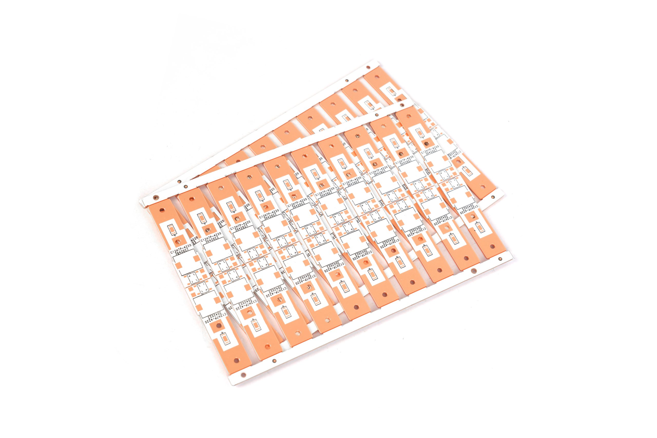
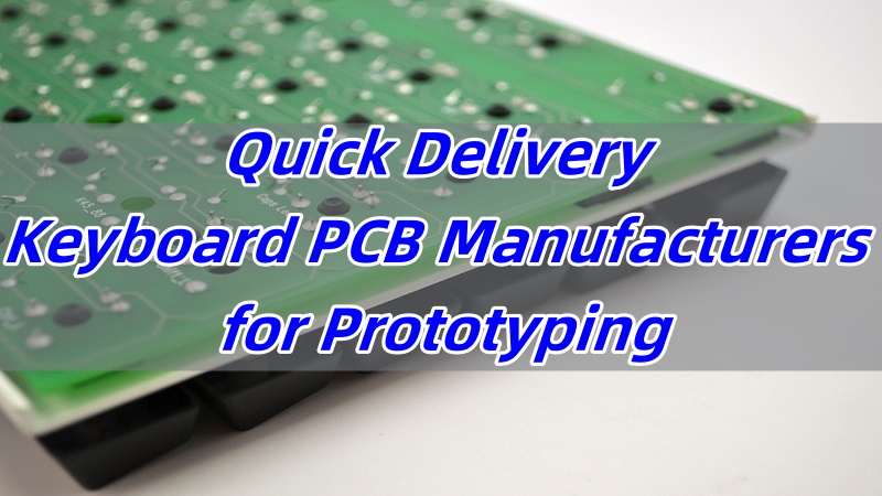
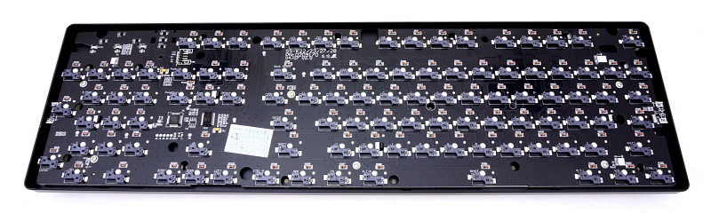
Keyboard PCB manufacturers are in high demand as the need for quick-turn prototyping rises. Especially for startups and custom mechanical keyboard makers, fast delivery and reliable service are key factors. In this blog, we’ll walk you through what keyboard PCBs are, their types, pricing, and how EBest Circuit (Best Technology) helps you avoid the most common production delays.
EBest Circuit (Best Technology) is one of the quick delivery keyboard PCB manufacturers for prototyping and assembly. We support flexible capacity from 10 pieces to 100 000pcs. You don’t need to worry about the MOQ issue. Moreover, EBest Circuit (Best Technology) suits your 72-hour prototyping delivery request in an urgent project. All the keyboard PCBs undergo the 72-hour aging test, which guarantees the quality. Besides, our SMT factories in China and Vietnam have given us a significant competitive edge in terms of production speed and cost. Our factories have the RGB SMD LED circuit impedance control technology (±5% tolerance) and our 8-layer PCB immersion gold process achieves a 1000Hzpolling rate.
EBest Circuit (Best Technology) provides a one-stop solution for custom PCB design, mechanical keyboard PCB manufacturing, firmware, and PCB assembly service. If you have any questions or would like to visit our factories, please contact us via call at +86-755-2909-1601 or email at sales@bestpcbs.com.
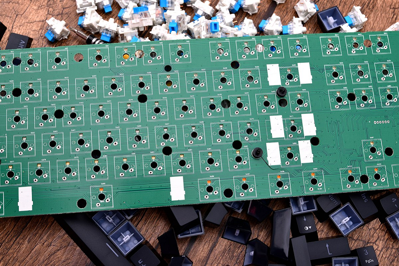
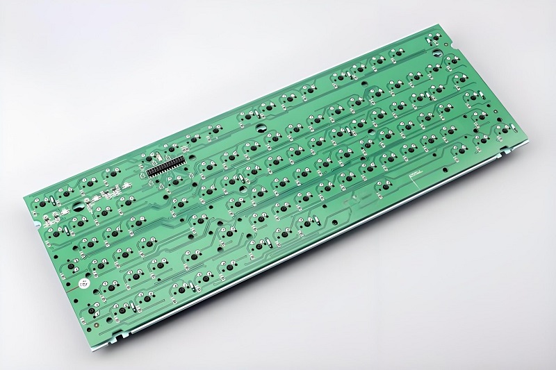
What Is a PCB Keyboard?
A PCB keyboard refers to the printed circuit board used at the core of every keyboard. This board connects switches, LEDs, and microcontrollers, managing keystroke data and power delivery. Unlike membrane alternatives, PCB keyboards are durable and provide better typing feedback. Whether it’s a gaming setup or a custom build, PCB keyboards give you control and reliability.
What Are Keyboard PCB Types?
There are several types of keyboard PCBs, each made to suit specific builds and experiences. Standard types include:
Hot-swappable PCBs: Allow switch changes without soldering.
Soldered PCBs: Permanent switch installation, often more stable.
Through-hole PCBs: Durable and suited for long-life mechanical builds.
Flexible PCBs: Designed for compact or curved applications.
Choosing the right type depends on how you want to build and maintain your keyboard.
Who Are Custom Keyboard PCB Manufacturers?
Custom keyboard PCB manufacturers cater to designers and enthusiasts who need unique layouts, LED setups, or additional controller logic. Companies like EBest Circuit (Best Technology) stand out by supporting full-stack services. We assist from design review and DFM (Design for Manufacturability) to final delivery, helping avoid delays due to common design flaws. With simulation tools and quick feedback, the process becomes smoother.
Who Are the Best Keyboard Manufacturers in the USA?
In the U.S., several firms provide quality mechanical keyboard PCBs, but the best combine technical support, fast turnaround, and real-time feedback. Makers like Input Club, Drop (formerly Massdrop), WASD Keyboards offer U.S.-based sales support, technical consultation, and strategic partnerships with local suppliers to avoid import delays. If you’re prototyping or building mid-volume batches, localized services make a big difference in timeline and cost.
What Is the Keyboard Circuit Board Price?
Prices for keyboard circuit boards vary based on layers, copper weight, board thickness, and layout complexity. For example:
2-layer boards: $2 – $5 per unit in bulk
4-layer boards: $5 – $10 per unit
Custom boards with 8+ layers and HDI may cost over $20 each
At EBest Circuit (Best Technology), our pricing remains competitive thanks to design standardization, smart material sourcing, and a tiered pricing structure to reduce costs as volume grows.
How Is a Keyboard PCB Manufactured?
Manufacturing involves several key steps:
Design review: Checking file formats (Gerber, CAD, etc.) and stack-up info
Paneling: Preparing the raw material with accurate thickness and copper weight
Impedance control: Especially for 4+ layers, signal integrity must be simulated and confirmed
Drilling & plating: Vias and through-holes are drilled and copper-plated
Solder mask & silk screen: Applying protective and labeling layers
Testing: Every board undergoes AOI and impedance verification
EBest Circuit (Best Technology) adopts 3D AOI and strict defect detection. We also pre-test for signal reliability in gaming-grade boards and offer aging tests to ensure performance longevity.
How to Choose Keyboard PCB Manufacturers?
When choosing a partner, prioritize:
Delivery speed: Can they provide 72-hour turnarounds?
Supply chain strength: Are there buffers for chip shortages?
Quality control: What’s their testing process?
Support: Do they offer project managers and live updates?
Experience: Have they built custom keyboard PCBs before?
EBest Circuit (Best Technology) checks all these boxes. With our prototype fast-track line, engineering feedback within 24 hours, and 100% impedance checks, your project stays on track.
Why Choose EBest Circuit (Best Technology) as One of Keyboard PCB Manufacturers?
Customers often face delayed deliveries due to part shortages, poor design feedback, or long engineering approval timelines. EBest Circuit (Best Technology) fixes these issues by:
Maintaining strategic inventory of key keyboard PCB components
Offering DFM reviews and signal simulations with tools
Deploying 24-hour engineering response teams and advanced inspection tools
Delivering a high-mix product line like single-sided PCBs, dual-layer PCBs, and multilayer PCBs. We will recommend the viable solutions as per your Keyboard construction and maintenance requirements.
Our warehouse strategy and work efficiency shorten delivery distances. For customers who need quick iterations, our 72-hour prototype service meets tight launch goals.
We also help reduce your costs by:
Using standard MX switch-compatible footprints
Reducing layers when possible for smaller layouts
Offering modular connector designs to lower customization costs
To top it all off, we provide one-on-one project managers, real-time production schedule sharing, and 24/7 support. These services keep communication clear and production fast.
Finally, when searching for reliable keyboard PCB manufacturers, speed, support, and precision are what matter most. EBest Circuit (Best Technology) offers all three. From handling global supply chain uncertainties to offering smart design suggestions, our goal is to make your keyboard project smoother. With fast turnaround, expert engineering, and strong quality systems, we’re the partner you can trust for both prototyping and volume production. If you have comments or suggestions please contact us via email at sales@bestpcbs.com or online customer service using the links here.
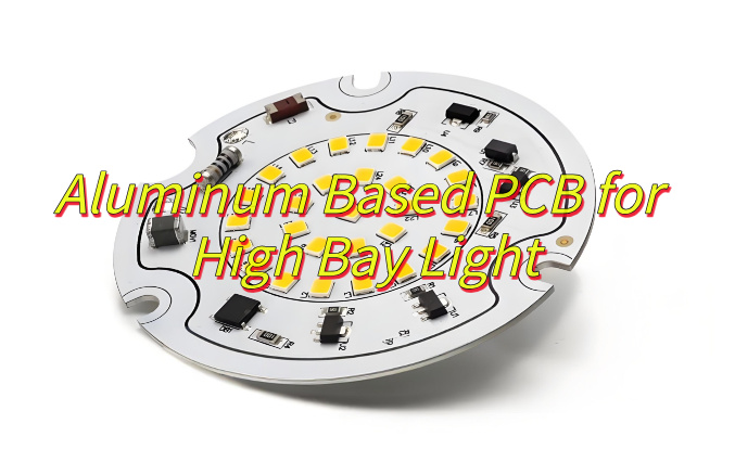
Looking for aluminum based PCB solution? This guide explores thermal management, performance enhancement, and long-term reliability strategies for optimal lighting solutions.
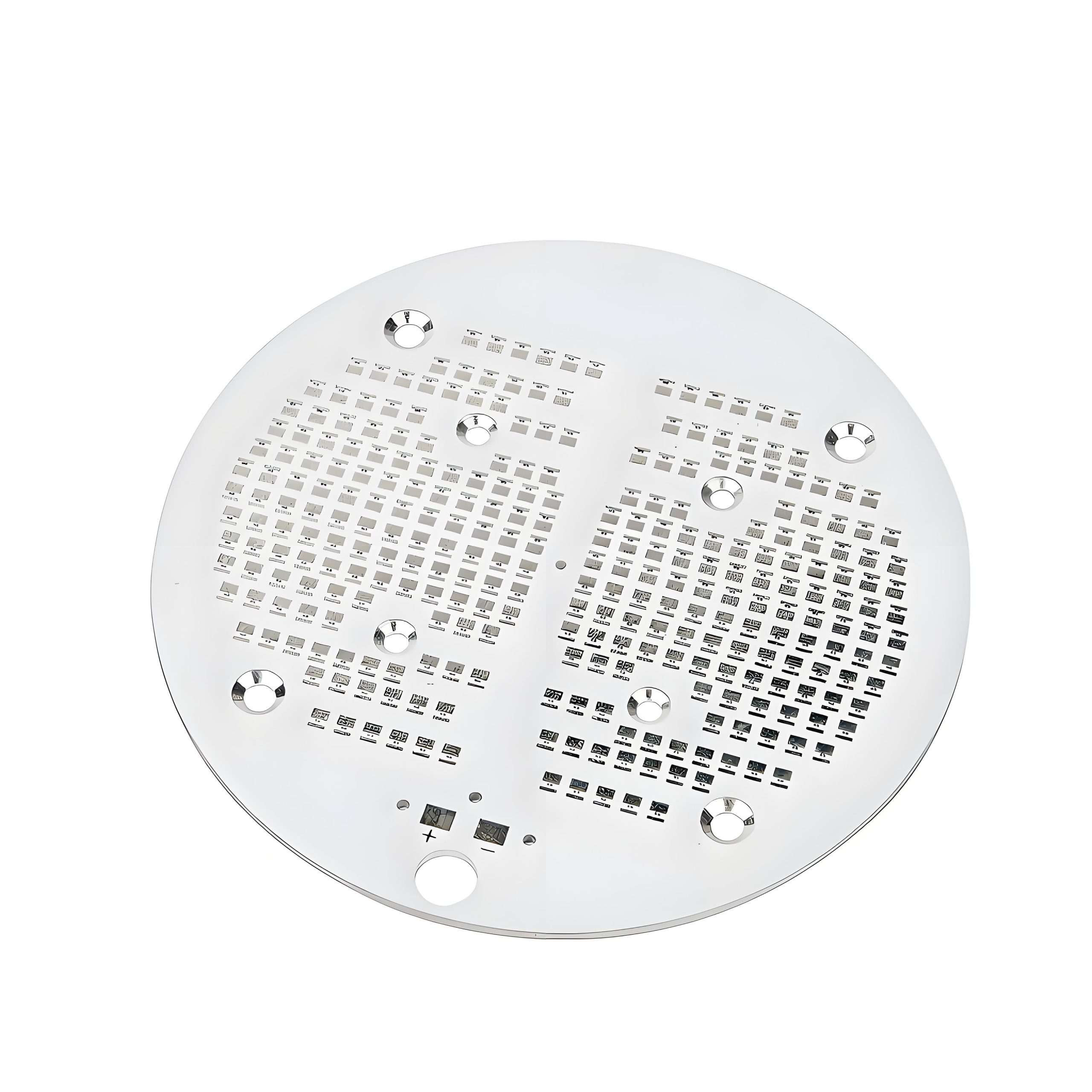
What Is Aluminum Based PCB?
An aluminum based PCBis a specialized circuit board that uses an aluminum substrate as its foundation instead of traditional fiberglass materials. The board’s structure typically includes three essential layers: a conductive copper layer for circuitry, a thermally conductive dielectric layer for electrical insulation, and the aluminum substrate that provides both mechanical support and heat dissipation.
This design offers superior thermal management compared to conventional PCBs, as the aluminum substrate efficiently transfers heat away from components. Similar to aluminum substrate PCB technology, these boards maintain excellent dimensional stability while operating in high-temperature environments. The metal core also provides natural electromagnetic shielding and vibration resistance.
Aluminum Based PCB Thermal Conductivity
Aluminum-based PCBs (Metal Core PCBs or MCPCBs) have a typical thermal conductivity ranging from 1.0 W/m·K to 8.0 W/m·K, depending on the dielectric layer composition. Here’s a detailed breakdown:
Factors Affecting Thermal Conductivity:
Dielectric Layer:
The thermally conductive but electrically insulating layer between the copper circuit and aluminum base is critical.
Standard dielectric: 1.0–2.5 W/m·K (e.g., epoxy-based).
High-performance dielectric (filled ceramics/polymers): Up to 8.0 W/m·K.
Aluminum Substrate:
Pure aluminum has high thermal conductivity (~220 W/m·K), but the dielectric layer limits overall performance.
Layer Thickness:
Thinner dielectric layers improve heat transfer but reduce electrical insulation.
Aluminum Based PCB Stackup
Aluminum-based PCBs(Metal Core Printed Circuit Boards) typically follow a 3-layer stackupoptimized for thermal management. Here’s the standard architecture:
Circuit Layer (Top)
Material: Copper foil (Electrodeposited or Rolled).
Heat Dissipation Solution for Aluminum Substrate Board
High-Conductivity Dielectric Layers: Select ceramic-filled polymer dielectrics (3–5W/m·K) to reduce thermal resistance. Optimize layer thickness (50–150μm) for balanced insulation and heat transfer.
Thermal Via Arrays: Place dense thermal vias (0.3–0.5mm diameter, 1mm pitch) under high-power components. Fill vias with silver epoxy or solder to boost vertical heat conduction.
Radiative Surface Treatments: Apply anodized coatings (10–30μm thickness) with emissivity >0.8 for radiative cooling. Use matte finishes to minimize heat reflection and enhance airflow.
Component Clustering: Position heat-generating devices (e.g., MOSFETs, LEDs) centrally on the board for uniform heat spreading. Maintain ≥2mm clearance from edges to prevent hotspots.
Direct Thermal Bonding: Attach components with thermally conductive adhesives (1–3W/m·K) or solder. Avoid low-conductivity TIMs (<0.5W/m·K) for critical high-power nodes.
Embedded Heat Spreaders: Integrate copper blocks or heat pipes into the aluminum substrate. Use press-fit or friction-stir welding for robust contact and rapid heat transfer.
Forced Convection Design: Align fins/channels on the aluminum surface with enclosure airflow. Include mounting holes for external heatsinks or fans (40–80mm diameter) to enhance cooling.
Why Choose Aluminum Based PCB for High Bay Light?
Reasons why choose aluminum base PCB for high bay light:
Thermal Efficiency: Conducts heat efficiently, reducing LED junction temperature by 20–30% (vs. FR-4), extending lifespan to 50,000+ hours.
Mechanical Strength: Supports heavy LED arrays/lenses, resists vibration and thermal expansion in harsh environments (e.g., factories).
Cost Savings: Eliminates external heatsinks/fans, cutting initial costs and long-term maintenance from thermal failures.
Compact Design: Allows dense component placement (e.g., multi-chip LEDs) without overheating, enabling slim fixtures for elevated/confined spaces.
Environmental Resilience: Corrosion-resistant, stable (-40°C to 150°C), ideal for outdoor/dusty industrial settings.
Energy Optimization: Stable thermal environment ensures consistent LED output, maximizing lumen/watt efficiency at higher drive currents.
How to Improve the Electrical Performance of Aluminum PCBs in High Bay lighting?
Thicken Copper Traces: Use 2oz–4oz copper to lower DC resistance, reducing voltage drop and heat in power lines. Supports 5A–20A currents without overheating.
Match Impedance: Design 50Ω microstrip lines with ground planes to minimize signal reflection. Critical for stable RF communication in dimming controls.
Isolate Power/Analog Circuits: Separate high-current drivers (e.g., MOSFETs) from low-noise analog sections. Prevents EMI coupling in LED control systems.
Ground Plane Bonding: Connect ground layers to aluminum via thermal vias. Enhances EMI shielding and heat dissipation simultaneously.
High-Voltage Insulation: Apply ≥100μm dielectric layers with >500V breakdown rating. Prevents arcing in AC-DC converter zones of mains-powered luminaires.
Low-ESR Capacitors: Select polymer/MLCC types (<10mΩ ESR) to stabilize driver outputs. Reduces ripple and extends lifespan under thermal stress.
Thermal-Electrical Co-Design: Use simulation tools to balance trace widths, via densities, and component placement. Avoids hotspots that degrade electrical reliability.
Long-Term Durability Strategies for Aluminum-Based PCBs in High-Bay Light
Material Durability: Use 5052/6061 aluminum alloys for corrosion resistance. Pair with polyimide dielectrics (Tg ≥150°C) to resist thermal degradation.
Vibration Resistance: Epoxy adhesive or fasteners secure heavy components. Optimized via placement distributes mechanical loads.
Humidity Control: Moisture-resistant solder masks (≥60μm LPI) and sealed edges prevent delamination. Store PCBs in dry packs (≤5% RH).
UV/Chemical Protection: UV-stable dielectrics/solder masks for outdoor use. Avoid chemical cleaners; use alcohol-based solvents.
Maintenance Protocols: Temperature sensors/thermal fuses detect overheating. Biannual inspections check for corrosion, cracks, or material wear.
Why Choose EBest Circuit (Best Technology) As Your Aluminum Based PCB Manufacturer?
Guaranteed Reliability – IPC Class 3 certified manufacturing with automated optical inspection (AOI) ensures <0.1% defect rates, preventing costly field failures in high-bay installations.
Transparent Cost Structure – No hidden fees with upfront pricing, including complimentary thermal simulations and DFM analysis to optimize designs before production.
Thermal Management Expertise – Free integrated heat-spreader solutions reduce LED junction temperatures by 15-30°C, extending luminaire lifespan without additional cooling components.
Industrial-Grade Durability – Anodized aluminum substrates with ceramic-filled dielectrics withstand 500+ thermal cycles (-40°C to 150°C), ideal for warehouses with extreme temperature swings.
One Stop Solution – Dedicated engineering team provides real-time production updates and technical guidance, streamlining procurement from prototype to volume orders.
If you have any request for aluminum based PCB, welcome to contact us: sales@bestpcbs.com.
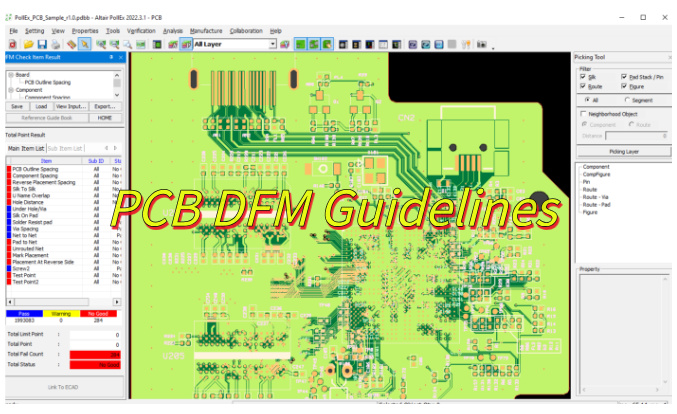
Why does PCB DFMmatter for reliable manufacturing? This guide covers design rules, layout strategies, and verification methods for optimized PCB production.
Does each engineering confirmation take 3-5 working days, slowing down the overall progress?
Do you know that more than 40% of the additional cost comes from process omissions in the design stage?
Can you afford the loss of the entire batch being scrapped due to undiscovered impedance deviation?
EBest Circuit (Best Technology) Can Provide:
Lightning DFM diagnosis: issue a 3D simulation report containing 267 process parameters in 12 hours (compared with peers in the industry in an average of 48 hours.
Cost sandbox simulation: use big data to predict the utilization rate of the board material, helping you save 8-15% of material loss.
Free engineering service: 24-hour online engineers answer your questions and avoid impedance deviation.
Welcome to contact us if you have any request for PCB design: sales@bestpcbs.com.
What Is PCB DFM?
PCB DFM(Design for Manufacturability) is a proactive approach to circuit board development that ensures designs can be efficiently and reliably manufactured. It involves analyzing layout elements such as trace widths, component spacing, via placement, and material choices to align with production capabilities while maintaining electrical performance.
By implementing DFM principles, designers avoid common pitfalls like insufficient solder mask clearance or unrealistic drill hole sizes that could lead to fabrication defects. The methodology also considers assembly requirements, ensuring proper thermal relief and component orientation for automated soldering processes.
This systematic verification reduces prototyping iterations, lowers production costs, and improves yield rates by addressing potential issues before manufacturing begins. Industry guidelines provide standardized benchmarks for implementing these checks throughout the design workflow.
PCB DFM Guidelines
Adopting DFM principles ensures PCB designs align with production capabilities, reducing errors and costs. Below are actionable guidelines for optimized manufacturing:
1. Layout Planning
Maintain ≥0.15mm (6mil) clearance between copper features to prevent solder bridges.
Place high-speed/RF components away from noise sources (e.g., switching regulators).
Use standard aspect ratios (e.g., 1:1 for SMT pads) to simplify assembly.
2. Component Placement
Position polarized components (e.g., electrolytic capacitors) with clear orientation markers.
Group similar parts (resistors, capacitors) to minimize pick-and-place time.
Avoid placing tall components (e.g., connectors) near board edges to prevent handling damage.
3. Solder Pad Design
Follow IPC-7351B standards for pad sizes (e.g., 0.5mm pitch QFN pads: 0.3mm solder mask opening).
Extend thermal pads on power components (e.g., MOSFETs) to improve heat dissipation.
Add solder paste stencils with 1:1 aperture-to-pad ratios for fine-pitch parts.
4. Trace Routing
Use ≥0.15mm (6mil) trace width for signals and ≥0.2mm (8mil) for power lines.
Avoid acute angles (<90°) to prevent acid traps during etching.
Isolate analog/digital grounds with single-point connections.
5. Via Design
Limit via-in-pad usage to reduce solder wicking (use filled/capped vias for BGA escape).
Maintain ≥0.25mm (10mil) annular ring to ensure via reliability.
Keep via aspect ratio (hole diameter: board thickness) ≤1:6 for plating consistency.
6. Thermal Management
Add ≥1mm² copper pours under power components (e.g., voltage regulators).
Include thermal vias (0.3mm diameter, 1mm pitch) to connect top/bottom layer heat sinks.
Avoid placing vias in thermal pad regions to prevent solder voiding.
7. Drill File Accuracy
Specify drill sizes in increments of 0.05mm (e.g., 0.2mm, 0.25mm).
Use separate files for plated (PTH) and non-plated (NPTH) holes.
Include a drill chart with tolerances (e.g., ±0.05mm for ≤0.5mm holes).
8. Silkscreen & Marking
Place reference designators ≥0.5mm away from pads to avoid solder mask interference.
Use high-contrast ink for silkscreen (e.g., white on green solder mask).
Include polarity marks for diodes, LEDs, and electrolytic capacitors.
9. Design for Assembly (DFA)
Minimize component count by using integrated devices (e.g., PMICs instead of discrete regulators).
Align SMT and THT components on the same side to reduce reflow passes.
Avoid mixing lead-free and leaded solder processes without manufacturer approval.
10. File Output & Validation
Generate Gerber files in RS-274X format with layer-specific extensions (e.g., .GTL for top copper).
Include a fabrication drawing with board outline, cutouts, and special instructions.
Run DFM checks using software tools (e.g., Valor NPI) to flag errors.
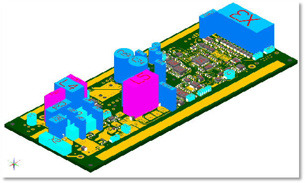
PCB DFM Layout Optimization Strategies
Component Placement Methodology
Functional grouping: Cluster components by circuit function (power, analog, digital) with at least 100 mil spacing between groups
Assembly considerations: Maintain 50 mil clearance around all components for pick-and-place machines
Thermal management: Position heat-generating components (voltage regulators, power ICs) with 200 mil spacing and access to thermal vias
Connector placement: Locate all board-to-board connectors within 300 mil of board edges
Signal Routing Best Practices
Trace geometry: Use 45° angles with minimum 3x width radius for bend transitions
Impedance control: Maintain consistent 5 mil spacing for differential pairs and reference planes
High-current paths: Implement 20 mil minimum width for 1A current carrying capacity
Noise isolation: Separate analog and digital grounds with at least 50 mil gap
Manufacturing Enhancement Features
Via standardization: Use 8 mil/16 mil (hole/pad) via sizes throughout the design
Solder mask: Apply 4 mil expansion on all SMD pads with 2 mil web minimum
Fiducial markers: Place three 40 mil diameter markers in L-shape pattern
Test points: Include 32 mil diameter test points every 5-10 components
Documentation Standards
Silkscreen: Use 45 mil height fonts with 7 mil line width
Layer identification: Mark all layers with orientation indicators
Version control: Include datecode and revision near board edge
Assembly drawings: Provide 1:1 scale component location diagrams
Design Validation Process
Run DRC checks with 6 mil minimum spacing rules
Verify annular rings meet 5 mil minimum requirement
Cross-check against manufacturer’s capability matrix
EBest Circuit (Best Technology) offers complimentary PCB DFM analysis reports to streamline your manufacturing process. Our automated system performs comprehensive design verification, checking 200+ manufacturing parameters against industry standards. You’ll receive detailed feedback on component spacing, trace widths, via placement, and other critical factors within 24 hours. This free service helps identify potential production issues before fabrication, reducing costly redesigns and delays. Simply upload your design files to receive a customized report with actionable recommendations. Our analysis covers all major fabrication aspects while maintaining strict data confidentiality. Take advantage of this professional evaluation to optimize your PCB design for manufacturability. Contact us now to get a free PCB DFM report:sales@bestpcbs.com.
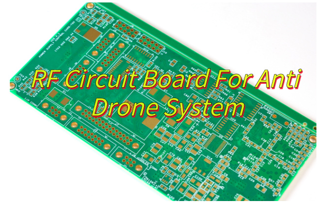
How can RF circuit boardrevolutionize anti-drone systems with their unique capabilities? This overview explores their design principles, environmental resilience, cost-efficiency, and full-band performance in counter-drone applications.
How to achieve an effective interference distance of 500 meters with a limited budget?
How to avoid signal interference causing false alarms from communication base stations?
Can it be compatible with mainstream drone frequency bands without interfering with GPS?
EBest Circuit (Best Technology) Can Provide You:
Stepped power enhancement service: Dynamic impedance matching technology improves antenna efficiency, and actual measurements show that it can extend the effective interference distance by 15%.
Base station signal collaborative analysis service: Adaptive notch filter is used to achieve 20ms-level rapid response to sudden base station signals.
Multi-protocol compatible solution: GPS L1 band out-of-band suppression reaches 55dB, and millimeter-level frequency band isolation is achieved through cavity filters.
Welcome to contact us if you have any request for RF circuit boards: sales@bestpcbs.com.
What Is A RF Circuit Board?
A RF circuit board is a specially engineered printed circuit board designed to transmit, receive, and process high-frequency radio signals, typically from a few megahertz (MHz) into the gigahertz (GHz) range and beyond. Unlike standard PCBs handling lower frequencies or digital signals, these boards require exceptional attention to signal behavior at high speeds.
They utilize specialized dielectric materials, such as PTFE (Teflon) or ceramic-filled laminates, chosen for stable electrical properties and minimal signal loss at RF frequencies. Precise control over trace geometries, impedance matching, grounding structures (like coplanar waveguides), and shielding techniques are fundamental. This careful design minimizes signal distortion, power loss (insertion loss), and unwanted radiation (EMI), ensuring signal integrity is maintained throughout the circuit path. RF circuit boards are essential components in wireless communication devices, radar systems, satellite technology, and high-speed test equipment.
Benefits of RF Circuit Boards
Superior High-Frequency Handling: RF circuit boards maintain signal quality across wireless frequencies from mobile networks to satellite communications, preventing degradation.
Precision Signal Management: Advanced designs minimize interference between components, ensuring stable connections in crowded electronic environments.
Temperature-Resistant Operation: Specialized materials prevent performance fluctuations during extended use or in extreme conditions.
Space-Efficient Architecture: Multi-layer construction allows complex circuitry in compact devices like wearables and IoT sensors.
Enhanced Durability: Manufactured to withstand environmental stressors including moisture, vibration, and thermal cycling.
Application-Specific Customization: Engineers can optimize designs for particular frequency ranges, power requirements, and physical constraints.
Energy-Efficient Performance: Optimized signal pathways reduce power waste, extending battery life in portable electronics.
Application of RF Circuit Board
5G RF Boards – Enable low-latency millimeter-wave data transfer in urban networks.
Medical RF Systems – Process high-precision signals for MRI/radiotherapy with thermal stability.
Automotive Radar Modules – Support 77 GHz collision detection and adaptive cruise control.
Satellite RF Components – Manage X/Ka-band signals for GPS and Earth observation in space.
IoT RF Connectivity – Provide Bluetooth/Wi-Fi links in smart devices with compact, low-power designs.
Military RF Tech – Jam signals and analyze spectrums with EMI-shielded high-power amplifiers.
Industrial RF Control – Enable wireless robot/AGV operation via interference-resistant frequency-hopping.
Consumer Electronics RF – Integrate cellular/Wi-Fi/GPS in smartphones with miniaturized, high-efficiency layouts.
How to Design RF Circuit Boards for Anti-Drone Jamming Systems?
Use FR-4 substrates for non-RF sections (e.g., control logic) to cut material expenses by 30–50%.
Reserve PTFE/ceramic laminates only for high-frequency traces (e.g., antenna feeds).
Simplified Layer Stackup
Design 4-layer boards (signal-ground-power-ground) instead of 6-layer.
Avoid blind/buried vias; use through-hole vias with staggered patterns for cost efficiency.
Automated Testing
Develop in-house test jigs (e.g., Arduino-based power meters) for basic checks (output power, harmonics).
Replace expensive spectrum analyzers with open-source tools (e.g., GNU Radio scripts) for signal validation.
Design Reuse
Create modular sub-boards (e.g., 2.4 GHz power amplifier module) repurposable across systems.
Standardize connectors (e.g., U.FL for RF, JST for power) to simplify inventory and repairs.
Thermal Management Trade-offs
Replace active cooling (fans, Peltier modules) with passive solutions (aluminum heat sinks + thermal pads).
Use stamped aluminum enclosures instead of machined magnesium for 40–60% cost reduction.
Regulatory Compliance
Pre-certify designs for unlicensed bands (e.g., 2.4 GHz Wi-Fi) to avoid redesign costs.
Use pre-compliance tools (e.g., USB spectrum analyzers with EMI filters) before formal testing.
Lifecycle Cost Reduction
Design for field repairability (socketed amplifiers, plug-in filters) to extend device lifespan.
Update firmware via USB/SD cards instead of hardware recalls (50–70% savings per update).
Why Choose EBest Circuit (Best Technology) as Your RF Board Manufacturer?
High-Frequency Precision Manufacturing – With ±0.025mm drilling accuracy and impedance control within 1%, we solve signal integrity issues in 5G/mmWave designs, backed by 67GHz testing.
Material & Process Expertise – 50+ qualified laminates (including ultra-low-loss Rogers/Duroid) and strict tan δ (<0.0015) control ensure consistent RF performance.
Thermal Reliability Solutions – Metal-core boards and embedded heat pipes (15W/cm² dissipation) prevent warping/delamination in high-power applications.
Rapid Prototyping & NPI Support – 24 hours prototype turnaround with DFM feedback within 4 hours accelerates your development cycle.
Supply Chain Security – 12-month buffer stock of critical materials and AS9100 logistics eliminate production delays.
Dedicated Engineering Partnership – Each project gets a senior RF engineer for real-time technical support from design to volume production.
Can RF Boards Overcome Full-Band Scanning Failures?
Yes, RF boards can overcome full-band scanning failures through design optimizations, signal processing, and environmental hardening. These strategies ensure reliable spectrum analysis even in noisy or dynamic conditions.
Signal Integrity Focus
Use impedance-matched microstrip lines (50 Ω ±5%) and via stitching to minimize signal loss, ensuring weak frequencies are detected during scans.
Integrate bandpass filters (e.g., SAW) to suppress out-of-band interference, improving signal clarity.
Dynamic Range Management
Deploy low-noise amplifiers (LNAs) with <1 dB noise figures to amplify faint signals without distortion.
Add automatic gain control (AGC) to adjust amplification levels dynamically, preventing saturation from strong nearby signals.
Redundant Scanning Paths
Design multi-channel architectures (e.g., dual independent receivers) to cross-validate results, reducing false negatives from single-channel issues.
Use RF switches to reroute signals to backup channels if anomalies are detected, ensuring continuous scanning.
Environmental Stability
Include temperature sensors and bias-adjustment circuits to stabilize amplifier performance across -40°C to +85°C, avoiding thermal drift.
Shield sensitive components (e.g., LNAs) with nickel-silver enclosures and EMI gaskets to block external interference.
Adaptive Software Tools
Embed self-calibration routines (e.g., frequency sweeps) to compensate for component aging or manufacturing variances.
Use FPGA-based processing to adjust scan parameters (dwell time, step size) in real time based on environmental feedback
By combining these approaches, RF boards deliver robust full-band scanning capabilities, making them reliable for anti-drone systems, spectrum monitoring, and wireless security applications.
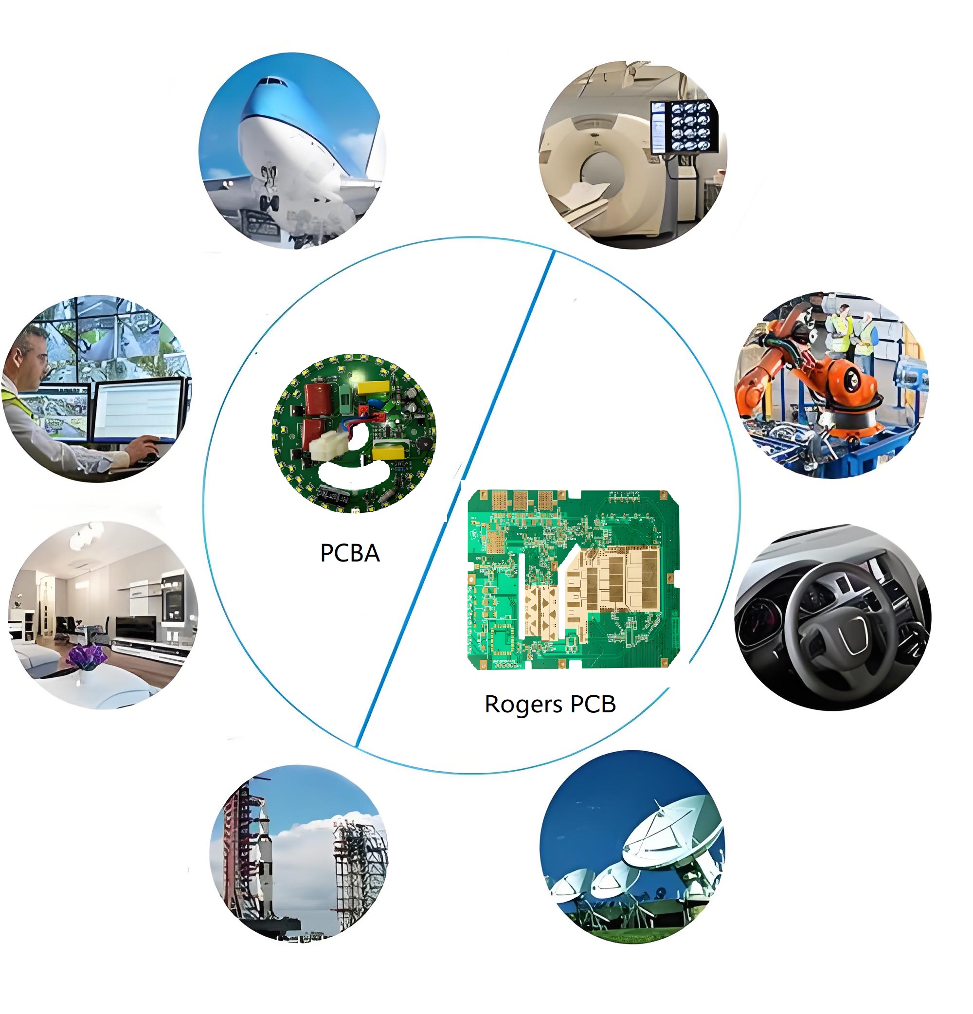
In EBest Circuit (Best Technology), the printed circuit Board manufacturing, particularly in high-frequency and high-speed signal transmission applications, Rogers Corporation’s PCB materials have become the go-to choice for our engineers. Rogers specializes in producing high-performance, highly reliable circuit board materials that find extensive use in wireless communications, automotive radar, satellite communication, and more. This blog post explores the unique advantages of Rogers PCBs and their significance in the international market.
What is Rogers PCB?
Rogers PCBs are renowned for their exceptional electrical performance. Compared to traditional FR-4 materials, Rogers materials offer a lower dissipation factor (Df), meaning they can maintain signal integrity at higher frequencies with reduced energy loss. This is critical for applications requiring precise data transmission such as 5G communications and millimeter-wave radars.
Rogers materials exhibit outstanding thermal stability. In high-temperature environments, these materials retain dimensional stability and mechanical strength, ensuring the reliability of PCBs under extreme conditions. For devices that need to operate stably over long periods, such as base stations or satellite communication equipment, this feature is especially important. Here is a comparison between Rogers materials and FR4.
Moreover, Rogers offers a range of materials with different characteristics to cater to various application needs. From low-loss to ultra-high-frequency applications, customers can choose the most suitable material based on their specific requirements. This not only enhances design flexibility but also provides more solutions to address complex engineering challenges.
In the context of globalization, competition in the international market has intensified. Utilizing Rogers PCB materials not only elevates the technical content and competitiveness of products but also offers customers a superior service experience. With the widespread adoption of 5G technology and the development of the Internet of Things (IoT), the demand for high-performance PCBs will continue to grow, making Rogers a leader in this field.
Advantages of Rogers PCB
1. Superior High-Frequency Performance
Rogers PCBs offer excellent electrical performance at high frequencies. Their stable dielectric constant and low loss tangent minimize signal loss and dispersion, which is critical for RF and microwave applications.
2. Low Dielectric Loss
Rogers materials have very low Df (dissipation factor), reducing power loss during signal transmission. This makes them highly efficient for high-speed, high-frequency signal paths.
3. Excellent Thermal Management
Rogers laminates have better thermal conductivity compared to standard FR4, allowing for more efficient heat dissipation. This helps maintain performance in demanding temperature environments.
4. Stable Electrical Properties
Their dielectric constant remains consistent over a wide range of temperatures and frequencies, enabling precise impedance control and signal integrity in advanced circuit designs.
5. Low Moisture Absorption
Rogers materials absorb less moisture than FR4, making them reliable for outdoor, aerospace, or high-humidity environments.
6. Better Reliability for Harsh Environments
With high temperature resistance and chemical stability, Rogers PCBs perform well in aerospace, military, and industrial applications where standard FR4 may fail.
Applications of Rogers PCB
1. RF and Microwave Circuits
Rogers PCBs are widely used in radio frequency (RF) and microwave communication systems, including antenna arrays, radar modules, and RF amplifiers.
2. 5G Infrastructure
Due to their low signal loss and excellent high-frequency characteristics, Rogers boards are ideal for 5G base stations, antennas, and network hardware.
3. Aerospace and Defense Systems
In aviation, satellites, and military electronics, Rogers PCBs provide the precision and durability needed for mission-critical communication and control systems.
4. Automotive Radar and ADAS
Modern vehicles use Rogers-based PCBs in advanced driver assistance systems (ADAS), radar sensors, and collision avoidance modules for reliable performance under extreme conditions.
5. Medical Imaging and Equipment
Rogers boards are used in MRI machines, RF ablation devices, and other diagnostic tools where consistent signal performance is crucial.
6. High-Speed Digital Circuits
In computing and telecommunications, Rogers materials support high-speed signal integrity for backplanes, routers, and high-frequency data transmission boards.
Conclusion
Rogers PCBs stand out globally due to their outstanding performance and broad applicability. Whether developing new communication devices or improving existing systems, choosing Rogers is a wise decision. Their commitment to innovation ensures they remain at the forefront of technological advancement, providing unparalleled solutions for tomorrow’s electronic challenges.
Best Tech is a very professional manufacturer in printed circuit board. If you are interesting to know more information for Rogers PCB and other high-speed signal transmission application for printed circuit board, please come to contact us at any time.
Ever wondered how microchip integrated circuit power our digital world? This guide covers their evolution, functions, manufacturing, applications, and performance evaluation.
Why does my chip solution always encounter welding failure and signal integrity problems during the PCBA stage?
How to solve the cost out-of-control caused by small batch and multi-variety production?
Why does the verification cycle from chip to complete machine always exceed expectations?
EBest Circuit (Best Technology) Can Provide You:
“Chip-PCBA joint simulation engine” – a collaborative simulation platform based on IBIS/SPICE models to predict welding stress and EMI risks in advance.
“Modular PCBA solution” – provides a standard package reference design library from QFN to BGA, increasing the patch yield by 30%.
Welcome to contact us if you have any request for PCBA: sales@bestpcbs.com.
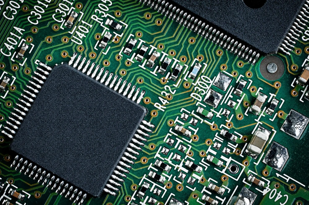
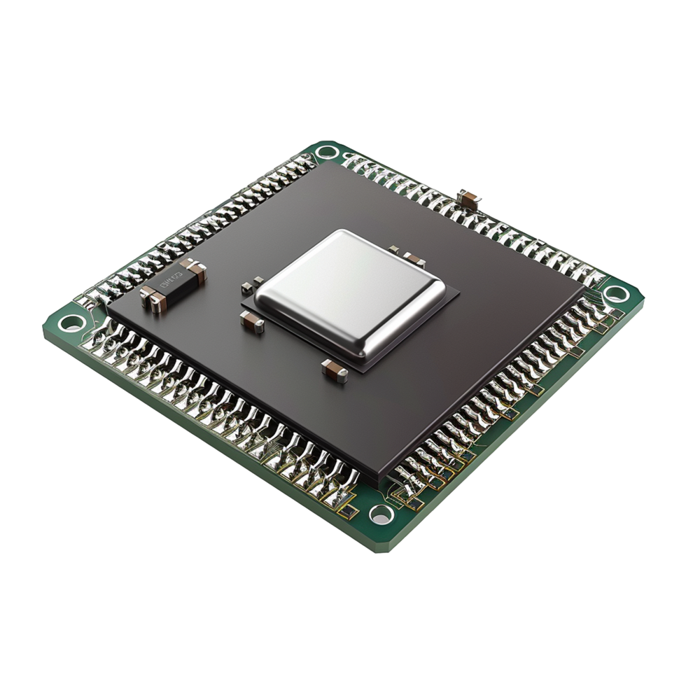
What Is Microchip Integrated Circuit?
A microchip integrated circuit, commonly known as a microchip or IC, is a miniaturized electronic structure fabricated on a single semiconductor substrate, typically silicon. It integrates essential components such as transistors, resistors, capacitors, and interconnecting pathways into a unified microscopic unit. This consolidation replaces bulky discrete circuits, enabling complex functionalities within compact physical dimensions. The microchip is encapsulated in protective housing (e.g., plastic or ceramic packages) with external pins for connectivity in broader electronic systems.
Draft schematics using EDA tools, simulate functionality and thermal behavior.
Validate logic gates, power distribution, and signal timing.
2. Silicon Wafer Production
Grow ultra-pure silicon crystals into ingots, slice into 300mm wafers.
Apply CMP to achieve <1nm surface roughness for patterning accuracy.
3. Photolithography
Coat wafers with photoresist, expose using UV light and reticle masks.
Develop patterns to 10nm resolution, defining transistor locations.
4. Etching
Remove unprotected silicon/metal via plasma or chemical etchants.
Create trenches for interconnects and transistor channels.
5. Doping
Implant boron/phosphorus ions using ion beam accelerators.
Diffuse dopants at 800–1200°C to form p-n junctions.
6. Thin Film Deposition
Use ALD to deposit 2nm insulating layers.
Apply CVD for copper seed layers in interconnects.
7. Interconnect Formation
Embed copper in damascene trenches, planarize with CMP.
Stack 8–12 metal layers for signal routing.
8. Defect Inspection
Scan wafers with SEM at 5000x magnification to detect cracks.
Use automated probes to test 10,000+ dies per wafer.
9. Wafer Dicing
Cut wafers into individual dies using laser ablation.
Collect dies with <10μm edge tolerance.
10. Packaging
Encapsulate dies in epoxy resin, attach solder bumps.
Integrate heat spreaders for thermal dissipation.
11. Final Testing
Perform burn-in tests at 125°C for 48 hours.
Grade chips by speed (GHz) and power (mW) metrics.
How to Evaluate the Performance of Microchip Integrated Circuits?
Performance evaluation priorities for microchip integrated circuits:
Speed & Responsiveness
Use oscilloscopes to measure signal propagation delay (ns) in critical paths.
Benchmark execution time for industry-standard tasks (e.g., AES encryption).
Power Consumption
Calculate dynamic power (switching activity × capacitance × voltage²) and static leakage.
Derive energy efficiency (nJ/operation) using precision power analyzers.
Thermal Stability
Perform thermal imaging under maximum load to identify hotspots (>85°C junction temp).
Validate thermal throttling thresholds and recovery time.
Signal Quality
Analyze eye diagrams for high-speed interfaces (e.g., PCIe Gen4) to assess jitter (<1ps RMS).
Measure noise margins using vector network analyzers.
Reliability Under Stress
Conduct 1,000-hour HTOL (High-Temperature Operating Life) tests at 125°C.
Inspect for electromigration in metal layers via SEM post-testing.
What Is the Lifespan of an Integrated Circuit Microchip?
The operational lifespan of integrated circuit microchips varies significantly based on application, operating conditions, and manufacturing quality, with typical functional longevity spanning 5–20 years under normal usage. Storage lifespan for unused chips under optimal conditions can exceed 10 years.
Operating Environment
Temperature: Sustained exposure above 85°C accelerates electromigration and material fatigue, reducing lifespan by up to 50%. Temperature cycling (repeated heating/cooling) induces mechanical stress in interconnects.
Electrical Stress: Voltage spikes or unstable power supplies degrade transistor gates and dielectric layers. Overclocking increases failure rates exponentially.
Humidity/Contaminants: Moisture ingress corrodes metal traces; airborne particulates cause short circuits.
Workload Intensity
High-Frequency Operation: Clock-intensive tasks (e.g., real-time data processing) accelerate electron migration in nanoscale interconnects.
Write/Erase Cycles: Flash memory chips withstand 10,000–100,000 cycles before storage degradation; controllers distribute wear to extend usability.
Manufacturing Factors
Process Node: Smaller nodes (e.g., 3nm/5nm) exhibit intensified aging effects like bias temperature instability due to atomic-scale structures. Larger nodes (e.g., 28nm+) typically offer higher longevity.
Material Quality: Impurities in silicon wafers or metal layers create weak points for early failure.
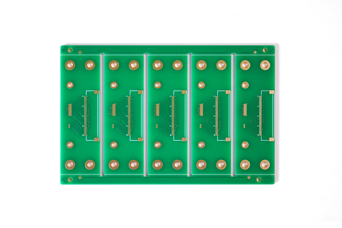
Dual layer PCB is often the top choice when balancing performance, cost, and compact design for both prototype and production. It’s ideal for engineers who need reliability without the complexity of multi-layer designs. In this blog, we’ll explore what it is, how it compares to other PCB types, and how EBest Circuit (Best Technology) helps you overcome real design and manufacturing challenges.
EBest Circuit (Best Technology) is a China EMS PCB manufacturer, presenting better quality dual layer PCB for prototype and assembly service to worldwide clients and markets. Our standard process for double layer PCBs supports a minimum finished board thickness of 0.2mm ±0.1mm, compatible with ENIG surface finish. For special requirements, we can produce boards with thicknesses ranging from 0.15mm to 0.4mm (±0.1mm) within a maximum size of 350×350mm. Our rigid PCB line varies, including heavy copper PCB, extra thin PCB, high Tg PCB, HDI PCB, and RF PCB. For any help, please contact our team by calling +86-755-2909-1601 or email at sales@bestpcbs.com.
What is a Dual Layer PCB?
A dual layer PCB, also called a double-sided PCB, has two copper layers—one on the top and another on the bottom. These layers are connected by plated through-holes. This structure allows for denser routing and more components compared to single layer boards. Dual-layer PCBs strike a strong balance between simplicity and capability.
What is the Difference Between Single and Double Layer PCB?
Single layer PCBs have components and routing only on one side. They are simple, low-cost, and easier to produce. But they can be limiting in complex circuits. Dual layer PCBs, by contrast, offer routing on both sides, providing more space and better electrical performance. For example, you can separate power and signal traces better, which improves noise control and makes debugging easier.
What is the Difference Between Dual Layer PCB and 4 Layer PCB?
A dual layer PCB has two copper layers, while a 4-layer PCB includes additional inner layers, usually for power and ground. This extra space gives better EMI shielding and more routing options. But it comes at a higher cost and longer lead time. Unless the circuit requires that added complexity, dual-layer designs are often more practical for cost-sensitive applications.
What are 2-Layer PCB Design Rules?
Effective design helps avoid signal problems and manufacturing defects. For a 2-layer PCB, key rules include:
Route high-speed signals near a ground plane to reduce interference.
Use decoupling capacitors near power pins to stabilize voltage.
Ensure impedance matching for differential pairs like USB or HDMI.
Minimize vias and layer transitions to keep costs low.
EBest Circuit (Best Technology)’s engineers help review your design before production to catch layout issues early. Our team uses automated DRC/DFM tools to prevent costly mistakes.
How Much Does a 2 Layer PCB Cost?
Prices depend on board size, copper thickness, surface finish, and order volume. On average, small batch prototype PCBs start at $30–$80, while larger production runs can bring per-unit cost below $1. At EBest Circuit (Best Technology), we offer cost control strategies like layout optimization, material selection (such as CEM-3), and bulk ordering for better pricing.
What is a Double Layer PCB Board Used For?
Double layer PCBs are used in a wide range of electronics. Common examples include:
Power supply modules
Lighting systems like LED drivers
Consumer electronics like smart devices
Industrial control boards
Their simplicity makes them easy to test and repair, yet they are robust enough for demanding use cases. With good layout, they can also handle moderate-speed signals and analog circuits.
Where to Get Dual-Layer PCB?
Choosing a reliable partner matters. EBest Circuit (Best Technology) provides dual layer PCB solutions tailored to your needs. We support prototyping, mass production, and turnkey assembly. Every board goes through electrical testing, visual inspection, and X-Ray for via quality. We also solve common pain points faced by engineers:
EMI issues? We suggest layout improvements and material selection to reduce noise.
Signal quality concerns? Our impedance control ensures clean signals for fast communication.
Soldering defects? We use AOI and X-Ray to catch issues before boards ship.
Our MES system ensures every component and batch is traceable—improving quality and simplifying troubleshooting.
In brief, dual layer PCBs are a great choice for prototypes and production alike. They offer a balance of performance and cost. But without proper design and process control, issues like signal loss, EMI, or soldering errors may arise.
EBest Circuit (Best Technology) solves customer needs with complete solutions: from layout optimization, precision drilling, automated assembly, to final testing. Whether you’re in automotive, medical, or consumer products, our team ensures your board meets every requirement. You can contact us at sales@bestpcbs.com, and be sure to give us Gerber files, quantity, and any special requirements so that we can quote you as fast as we can.
This website uses cookies to enhance your experience, remember your preferences, and help us understand how visitors use our site. You can accept all cookies, reject non-essential cookies, or manage your settings.
This website uses cookies to improve your experience while you navigate through the website. Out of these cookies, the cookies that are categorized as necessary are stored on your browser as they are essential for the working of basic functionalities of the website. We also use third-party cookies that help us analyze and understand how you use this website. These cookies will be stored in your browser only with your consent. You also have the option to opt-out of these cookies. But opting out of some of these cookies may have an effect on your browsing experience.
Necessary cookies are absolutely essential for the website to function properly. These cookies ensure basic functionalities and security features of the website, anonymously.
Cookie
Duration
Description
cookielawinfo-checkbox-analytics
11 months
This cookie is set by GDPR Cookie Consent plugin. The cookie is used to store the user consent for the cookies in the category "Analytics".
cookielawinfo-checkbox-functional
11 months
The cookie is set by GDPR cookie consent to record the user consent for the cookies in the category "Functional".
cookielawinfo-checkbox-necessary
11 months
This cookie is set by GDPR Cookie Consent plugin. The cookies is used to store the user consent for the cookies in the category "Necessary".
cookielawinfo-checkbox-others
11 months
This cookie is set by GDPR Cookie Consent plugin. The cookie is used to store the user consent for the cookies in the category "Other.
cookielawinfo-checkbox-performance
11 months
This cookie is set by GDPR Cookie Consent plugin. The cookie is used to store the user consent for the cookies in the category "Performance".
viewed_cookie_policy
11 months
The cookie is set by the GDPR Cookie Consent plugin and is used to store whether or not user has consented to the use of cookies. It does not store any personal data.
Functional cookies help to perform certain functionalities like sharing the content of the website on social media platforms, collect feedbacks, and other third-party features.
Performance cookies are used to understand and analyze the key performance indexes of the website which helps in delivering a better user experience for the visitors.
Analytical cookies are used to understand how visitors interact with the website. These cookies help provide information on metrics the number of visitors, bounce rate, traffic source, etc.
Advertisement cookies are used to provide visitors with relevant ads and marketing campaigns. These cookies track visitors across websites and collect information to provide customized ads.