- Are you still disrupting your production plan because of the unstable delivery time of PCB suppliers?
- The high cost and long cycle of BOM procurement slow down your product launch speed?
- During small-batch trial production, have you encountered repeated design modifications caused by process mismatch?
EBest Circuit (Best Technology) Can Provide:
- On-time delivery guarantee: intelligent production scheduling system + safety inventory, on-time delivery rate of 99.2%, daily compensation for breach of contract.
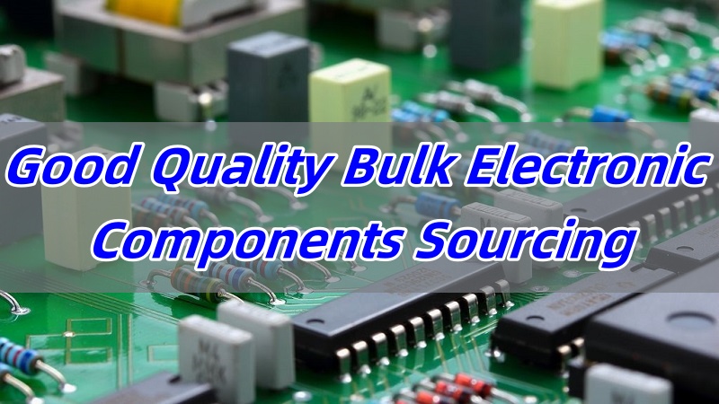
- Supply chain integration: 200+ global component strategic cooperation, 48-hour ultra-fast procurement of commonly used materials, and 15% cost reduction.
- Free DFM optimization: 24-hour manufacturability report is provided to avoid repeated proofing caused by design defects.
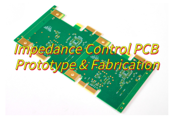
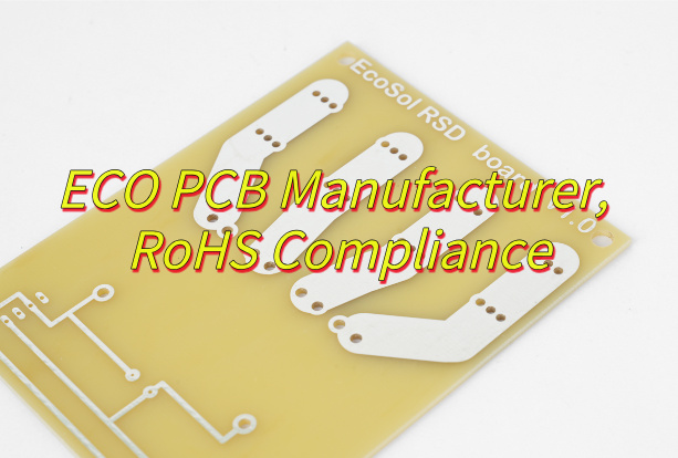
Welcome to contact EBest Circuit (Best Technology) if you have any request for turnkey PCB assembly or PCBA: sales@bestpcbs.com.
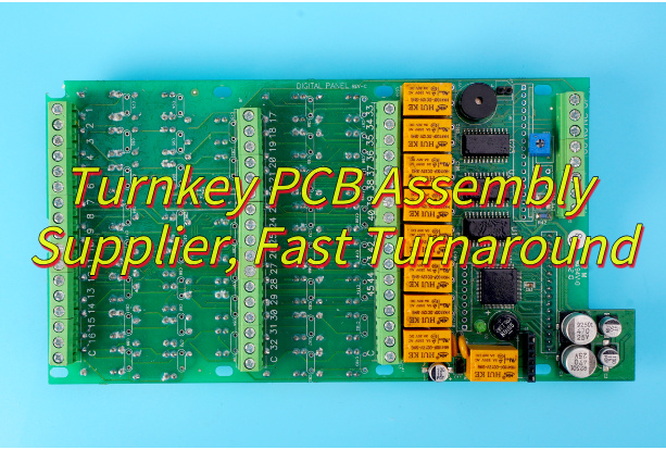
Why Choose EBest Circuit (Best Technology) as Your Turnkey PCB Assembly Supplier?
Here are the reasons to choose EBest Circuit (Best Technology) as your turnkey PCB assembly supplier:
- Fastest Turnaround – Industry-leading production cycles (prototypes in 24-48 hours, volume orders in 5-10 days)
- Reliable Quality – Certified IPC-A-610 Class 3 standards with 99.98% first-pass yield rate
- Competitive Pricing – Cost-optimized solutions without compromising quality (15-30% savings vs. industry averages)
- Stable Supply Chain – Long-term partnerships with component manufacturers ensuring material availability
- Rapid Response – Dedicated engineering support with 1-hour initial response times
- Flexible Scaling – Seamless transition from prototypes to mass production
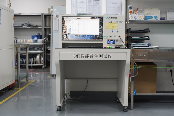
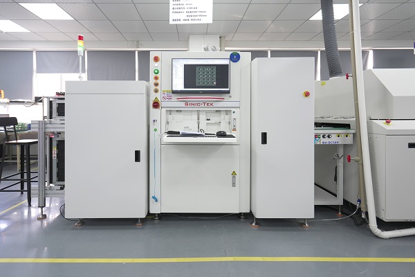
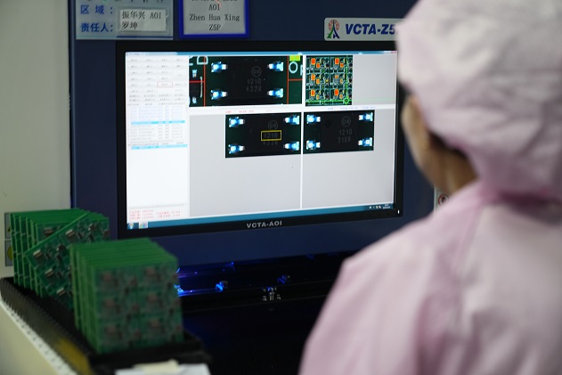
- Comprehensive Testing – Automated optical inspection (AOI), functional testing, and full traceability
- Technical Expertise – 15+ years of experience handling complex designs (HDI, flex, RF, etc.)
- Transparent Communication – Real-time production updates through client portal
- Risk Mitigation – Dual-source procurement and buffer inventory for critical components
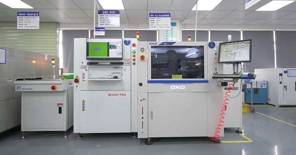
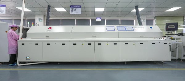
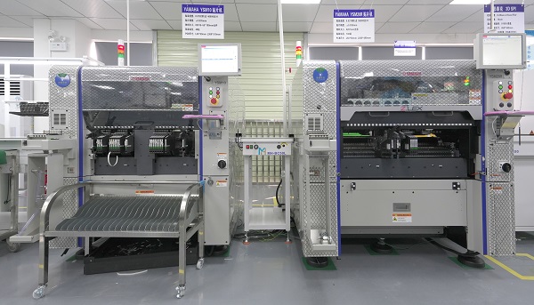
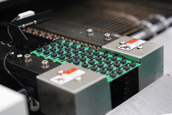
Our PCB Assembly Capacities
| Item | Capabilities |
| Placer Speed | 13,200,000 chips/day |
| Bare Board Size | 0.2 x 0.2 inches – 20 x 20 inches/ 22*47.5 inches |
| Minimum SMD Component | 01005 |
| Minimum BGA Pitch | 0.25mm |
| Maximum Components | 50*150mm |
| Assembly Type | SMT, THT, Mixed assembly |
| Component Package | Reels, Cut Tape, Tube, Tray, Loose Parts |
| Lead Time | 1 – 5 days |
Our Quality Inspection & Certifications
- Certified & Compliant Standards: ISO 9001, ISO 13485, IATF 16949, AS9100D Certified, and UL, REACH, RoHS Compliant.
- AOI (Automated Optical Inspection): Detects surface defects like open/short circuits, missing components, and soldering issues. X-Ray Inspection (Internal Defect Screening): Checks solder joint voids, cracks, and BGA/QFN hidden defects.
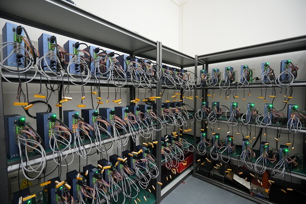
- Aging Test (Environmental Stress Screening): Includes thermal cycling (-40℃~85℃) and humidity exposure to validate long-term reliability.
- Salt Spray Test (Corrosion Resistance): Evaluates coating durability under 5% NaCl solution (≥72 hours).Dimensional Verification (CMM/Profilometer): Measures thickness (±0.1mm), flatness, and hole alignment accuracy.
- Peel Strength Test (Adhesion Assessment): Quantifies copper-clad laminate bonding force (ASTM D903).
Our Turnkey PCB Assembly Service Options
Here are our turnkey PCB assembly service options:
- One-Stop Solution – Includes PCB manufacturing, component sourcing, assembly, and testing in a single integrated service.
- Quick-Turn Prototyping – Accelerated production of assembled PCB prototypes to reduce time-to-market.
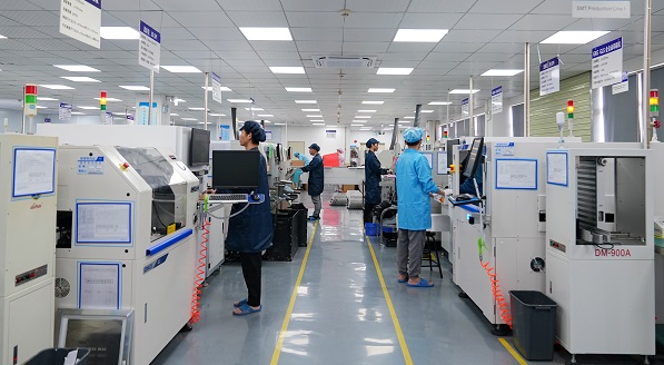
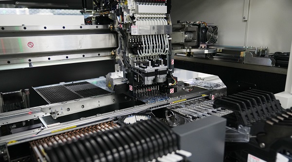
- SMT Assembly – High-precision surface mount technology for accurate placement of miniature components.
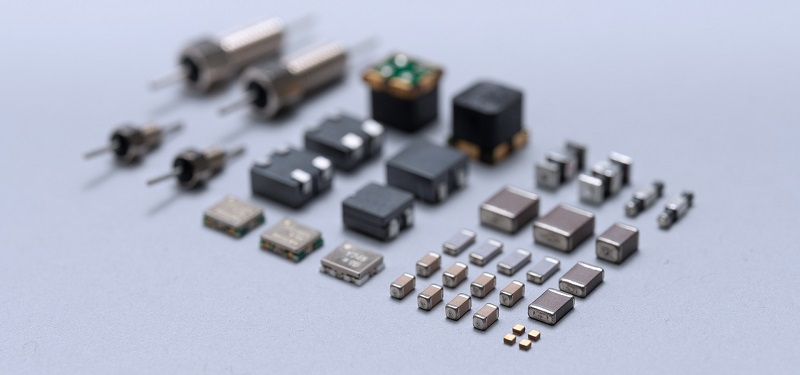
- Component Procurement – Global supply chain management with access to 100,000+ in-stock parts and risk-mitigated sourcing.
- Design Support – Professional engineering assistance from design (DFM/DFX) to manufacturing.
- Quality Assurance – Full production monitoring with advanced testing and QMS protocols.
What Is Turnkey PCB Assembly?
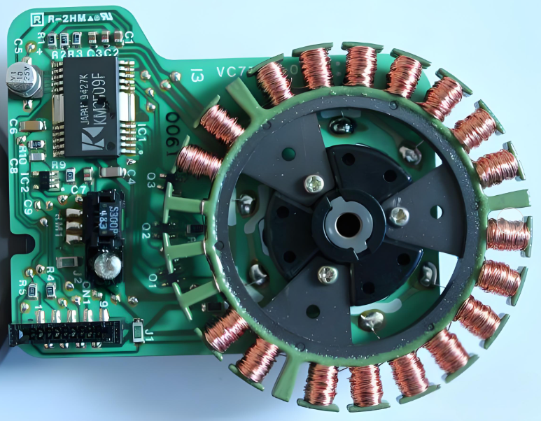
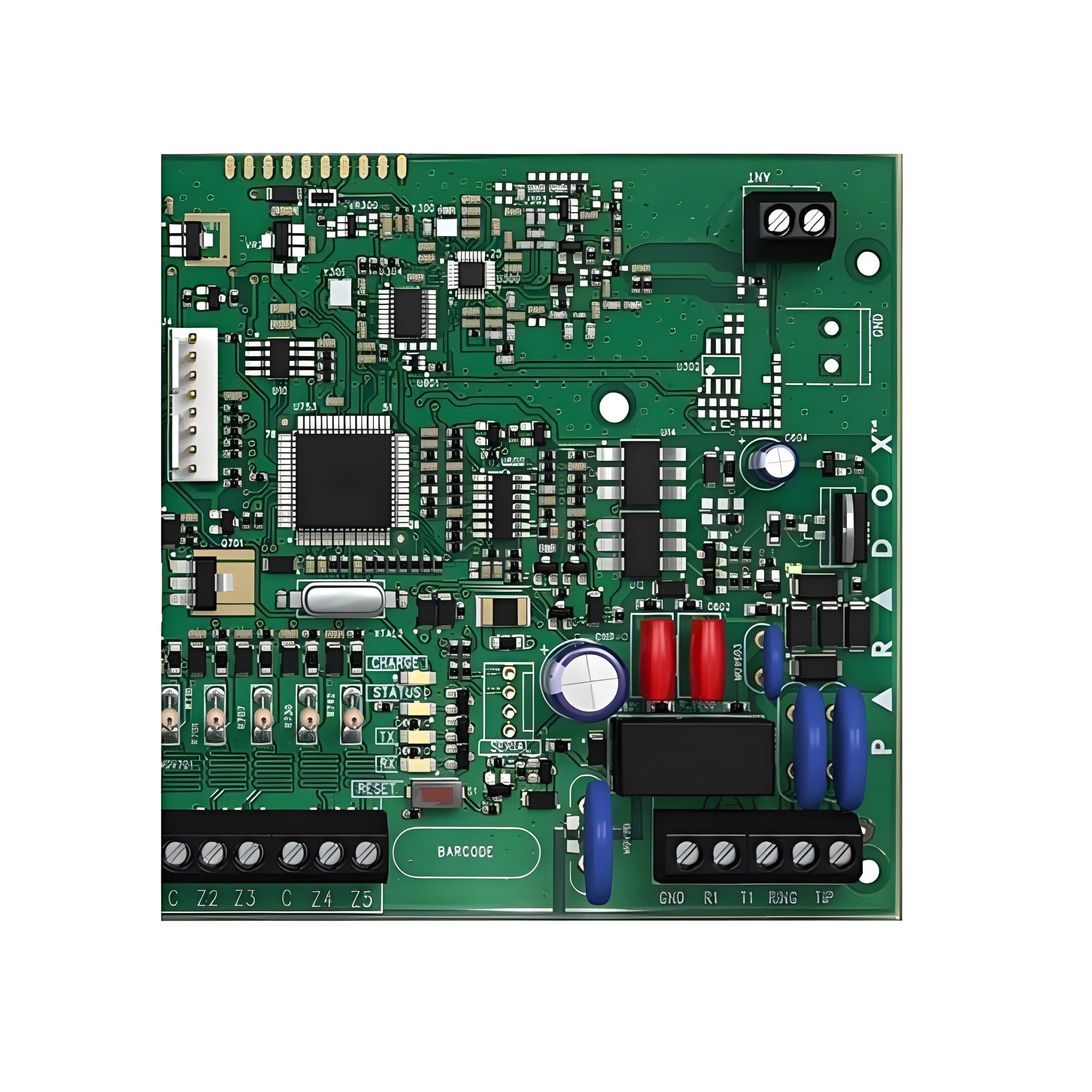
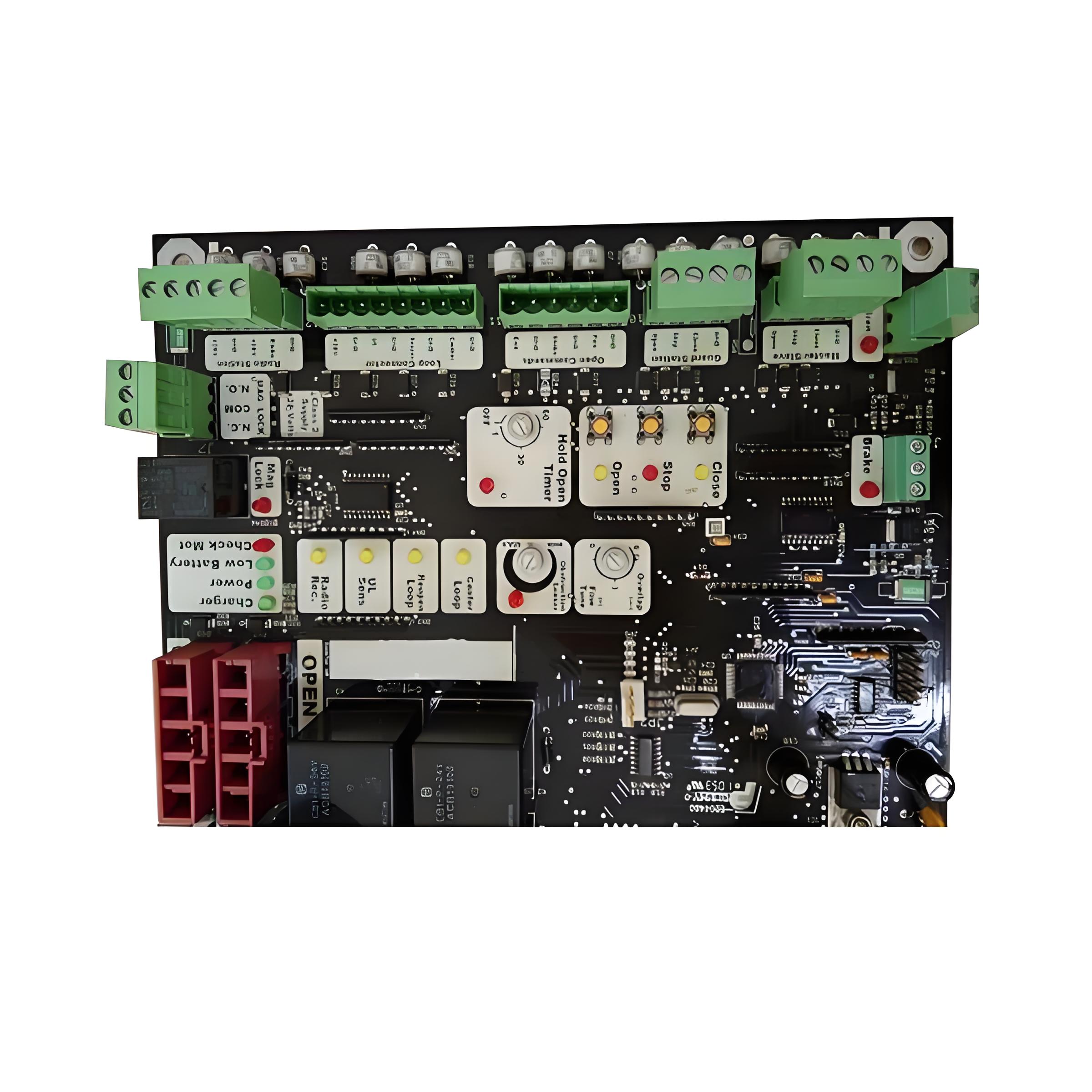
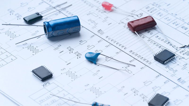
Turnkey PCB assembly(PCBA) is a complete manufacturing service where a provider handles every step of printed circuit board production, from initial design review to final delivery. This integrated approach includes component sourcing, PCB fabrication, assembly, testing, and quality control, allowing clients to receive fully functional boards without managing multiple vendors.
The process begins with design verification to ensure manufacturability, followed by procurement of all necessary materials. Advanced pick-and-place machines then populate the board, with thorough inspection at each stage. Automated testing procedures validate electrical performance before shipment.
This service model reduces logistical complexity, minimizes supply chain risks, and accelerates time-to-market. It eliminates the need for clients to maintain inventory or coordinate between separate fabrication and assembly facilities, providing a streamlined solution for prototypes or production-scale orders.
The Benefits of Turnkey PCB Assembly
End-to-End Process Control
- Single-point responsibility for design verification, component procurement, assembly, and testing.
- Eliminates coordination gaps between multiple vendors.
Cost Efficiency
- Bulk purchasing power reduces material costs by 15-30%.
- Automated assembly minimizes labor expenses.
Faster Time-to-Market
- Concurrent engineering processes shorten development cycles.
- Typical lead times reduced by 40% compared to fragmented sourcing.
Quality Assurance
- Integrated testing protocols (ICT, flying probe, functional testing).
- Traceability systems track every component from sourcing to final assembly.
Technical Expertise
- DFM analysis prevents 80% of common manufacturing issues.
- Support for advanced packaging (01005, 0.2mm pitch BGA).
Supply Chain Reliability
- Managed inventory buffers against component shortages.
- Alternative sourcing plans for obsolete parts.
Scalability
- Seamless transition from prototype (10 units) to mass production (100k+).
- No requalification needed between phases.

What Is the Difference Between Consigned and Turnkey?
| Operational Aspect | Consigned Assembly | Turnkey (Full-Service) Assembly |
| Component Provision | Client manages sourcing of all parts | Manufacturer handles all material procurement |
| Material Accountability | Client retains ownership of parts inventory | Manufacturer assumes material ownership |
| Supply Chain Management | Client controls entire component logistics chain | Single-point supplier coordination |
| Cost Structure | Payment limited to assembly labor/services | Comprehensive pricing (components + assembly) |
| Component Verification | Client performs authenticity/certification checks | Manufacturer verifies all materials |
| Production Initiation | Requires client-delivered components for start | Manufacturer initiates without client materials |
| Quality Dispute Resolution | Shared responsibility between parties | Unified supplier accountability |
How to Get a Quote for Turnkey PCB Assembly Service?
Here’s a practical guide to obtaining accurate quotes for turnkey PCB assembly services:
1. Prepare Essential Documentation
- Complete PCB design files (Gerber/ODB++, BOM, centroid/pick-and-place).
- Technical specifications (PCB material, thickness, surface finish).
- Quantity requirements (prototype, small-batch, or mass production).
- Testing/QC requirements (ICT, flying probe, functional testing).
2. Information to Specify
- Board complexity (layer count, component density).
- Component types (standard, high-temperature, fine-pitch).
- Special requirements (conformal coating, potting, box-build).
- Certifications needed (ISO, UL, IPC standards).
3. Submission Process
- Upload files to supplier’s secure portal (preferred method).
- Email packages with clear subject line (“RFQ for 6-layer medical PCB assembly”).
- Complete online quote request forms with dropdown selections.
4. Timeline Expectations
- Standard quotes: 24-48 hour turnaround.
- Complex projects: 3-5 business days.
- Expedited quotes: Available for urgent projects (typically +15-20% fee).
5. Quote Evaluation Factors
- Breakdown of material/labor costs.
- MOQ (minimum order quantity) pricing tiers.
- Lead time commitments.
- Warranty terms (typically 1-2 years).
- ECO (engineering change order) policies.
Conclusion
Turnkey PCB assembly provides a streamlined solution from design to finished product, eliminating supply chain complexities while ensuring quality and faster time-to-market. For reliable production with certified standards, competitive pricing, and rapid turnaround (prototypes in 24-48 hours), contact EBest Circuit (Best Technology) for a detailed quote today. Submit your Gerber files and BOM via our instant quote system to start your project. Ready to proceed? Request your quote now: sales@bestpcbs.com.