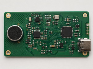
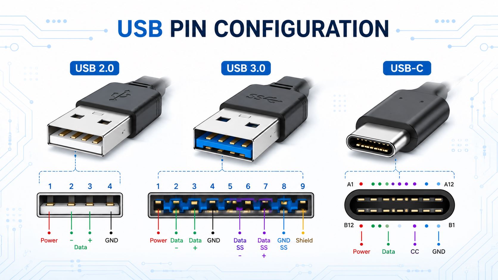
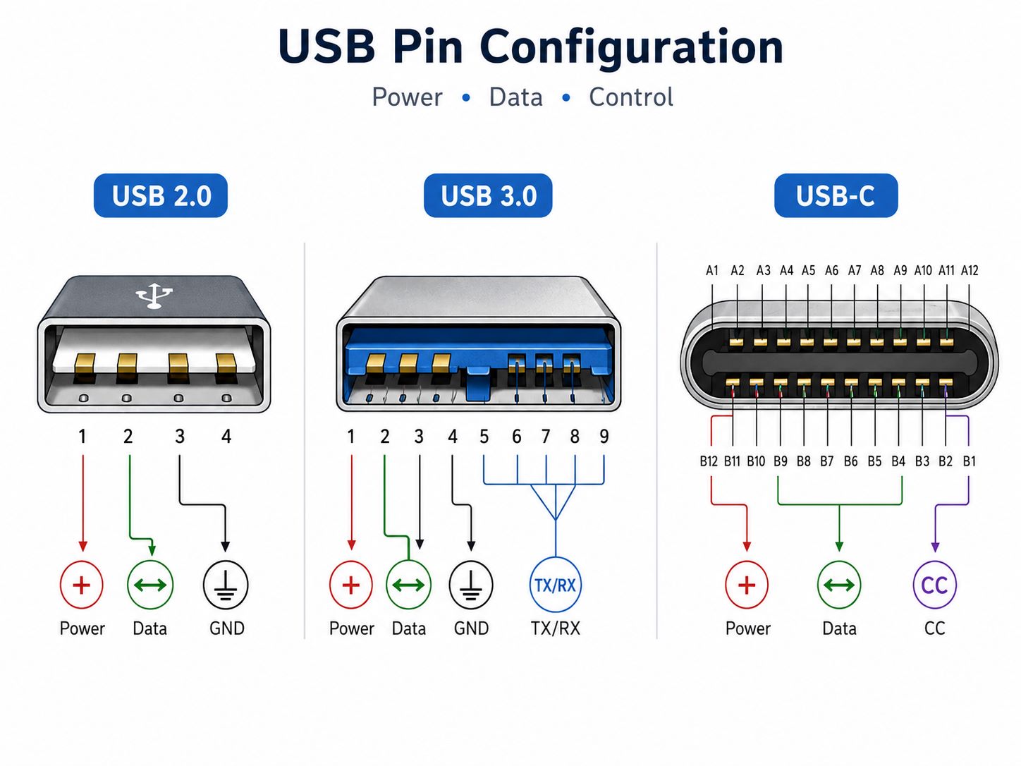
Pin configuration of USB port connectors determines how power, ground, and data signals are assigned inside a USB interface. USB ports are used in chargers, laptops, control boards, industrial devices, and consumer electronics, but a small pin or routing mistake can lead to charging failure, unstable data transfer, or connector reliability issues. This blog explains USB 2.0, USB 3.0, USB-C pin layouts, USB wire color codes, and the key PCB layout and assembly points engineers should check before moving a USB-related board into production.
What Is the Pin Configuration of a USB Port?
The pin configuration of USB port connectors describes how each electrical contact inside a USB connector is assigned. Some pins provide power. Some pins connect to ground. Some pins carry data signals. In newer USB interfaces, extra pins may also support high-speed transmission, plug orientation detection, current identification, and power negotiation.
In simple terms, a USB pin configuration tells you what each pin does and how it should be connected in a cable, device, or PCB. For example, a basic USB 2.0 port normally uses VBUS, D−, D+, and GND. USB 3.0 adds more pins for SuperSpeed data. USB-C uses a more advanced 24-pin structure that supports reversible plugging, higher current capability, and more flexible functions.
For PCB projects, USB pin configuration is not just a drawing. It affects the schematic, connector footprint, PCB routing, ESD protection, soldering strength, inspection method, and final product reliability. A small connector mistake can cause charging failure, unstable data transfer, or a USB port that works only in certain conditions.
That is why engineers and buyers should check the USB pinout, connector datasheet, PCB layout, and assembly requirements before prototype or mass production.
USB Port Pin Configuration Diagram and Basic Pin Functions
Before looking at USB 2.0, USB 3.0, and USB-C separately, it helps to understand the common USB signal names. Different connectors may have different pin counts, but many USB ports share similar electrical functions.
| Signal | Basic Function |
|---|---|
| VBUS | Power |
| GND | Ground |
| D+ | USB 2.0 data + |
| D− | USB 2.0 data − |
| TX+ / TX− | High-speed transmit |
| RX+ / RX− | High-speed receive |
| CC1 / CC2 | USB-C detection |
| SBU1 / SBU2 | Alternate mode |
| Shield | EMI support |
The most basic USB interface only needs power, ground, and one pair of data lines. More advanced USB ports add extra pairs for higher data speed. USB-C also adds CC pins, which are important for cable orientation and current detection.
For PCB layout, these pins are not equal in difficulty. VBUS and GND mainly need proper current capacity. D+ and D− need clean differential routing. USB 3.0 TX/RX pairs need tighter impedance control. USB-C CC pins need correct connection, even when the port is only used for power input.
A useful way to understand USB pin configuration is this:
- Power pins decide whether the device can charge or receive power.
- Ground pins provide the return path and signal reference.
- Data pins decide whether the device can communicate.
- High-speed pins decide whether fast transfer is stable.
- Configuration pins decide how USB-C detects the cable and connection.
- Shield pins help with mechanical strength and EMI control.
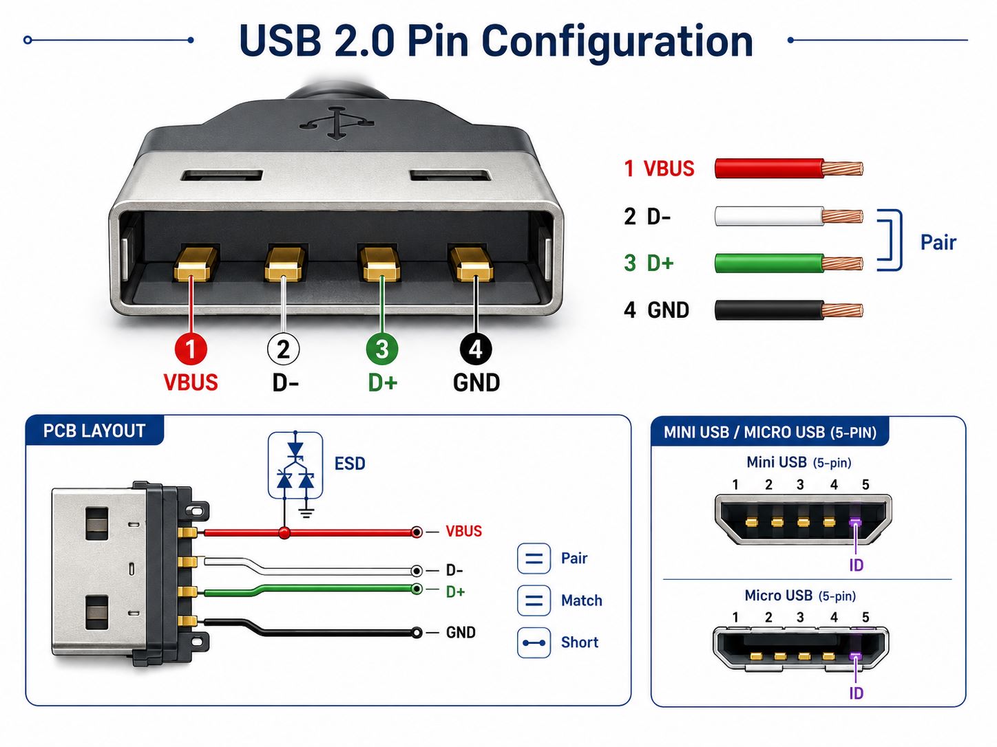
USB 2.0 Pin Configuration
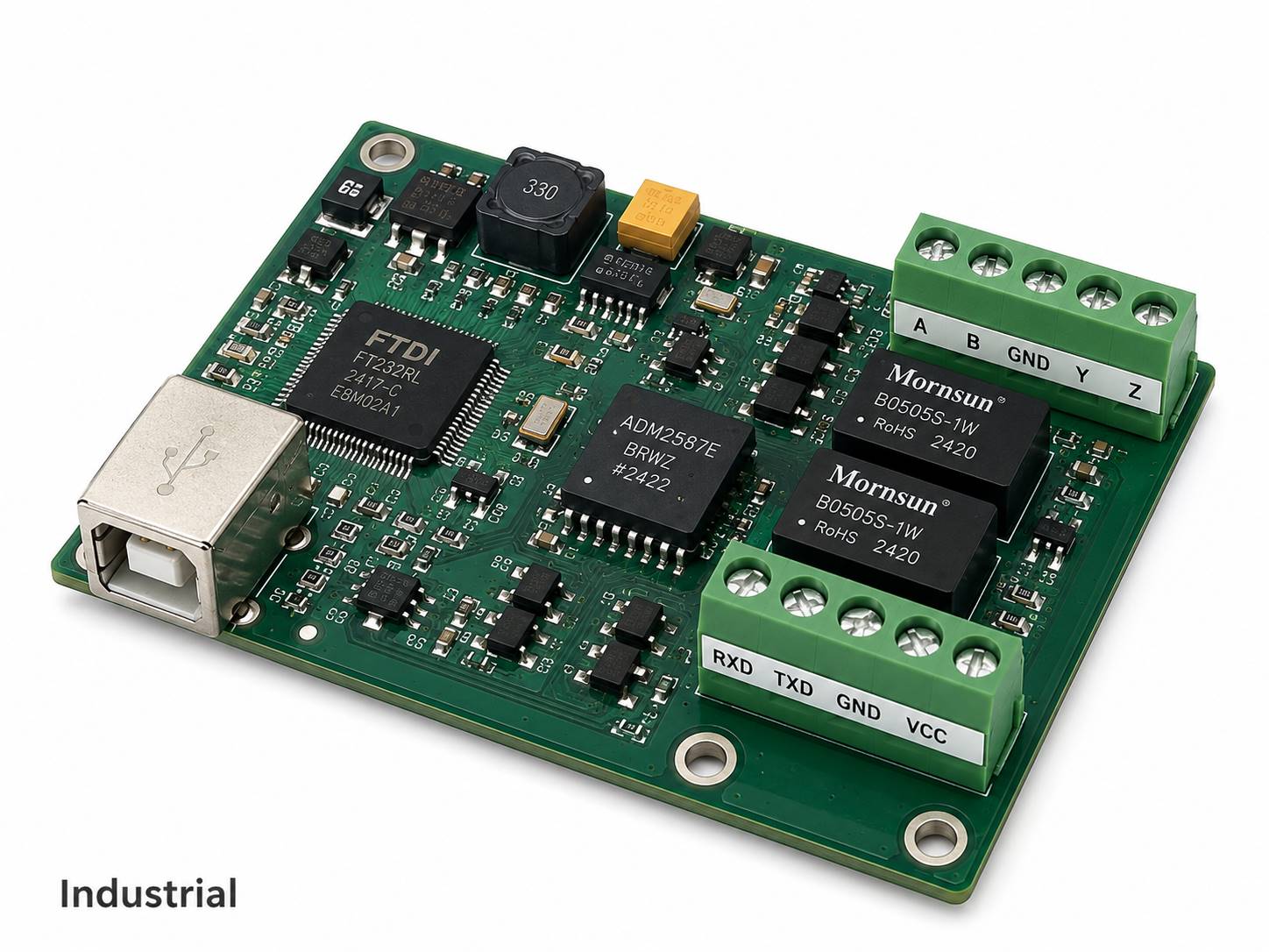
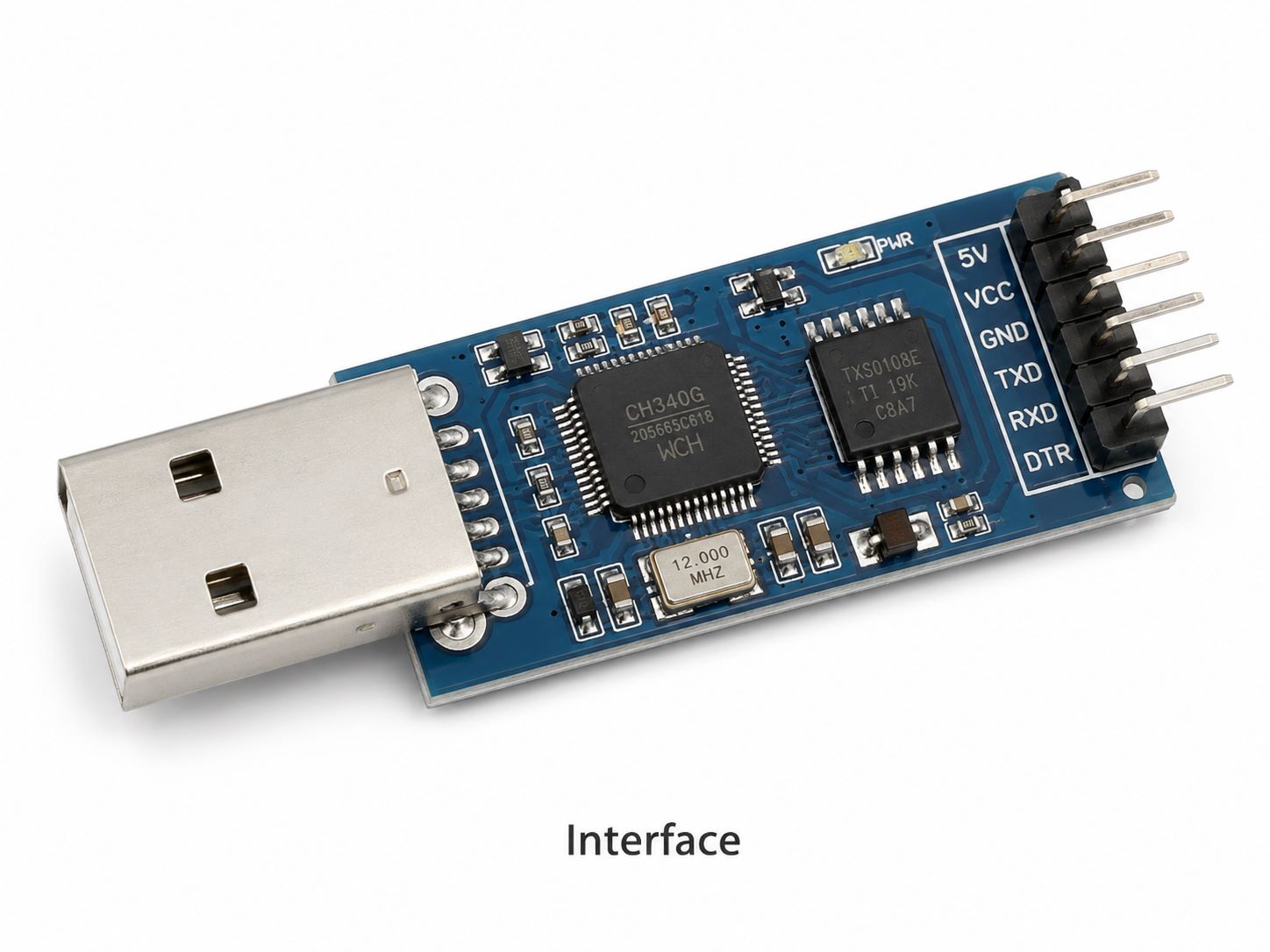
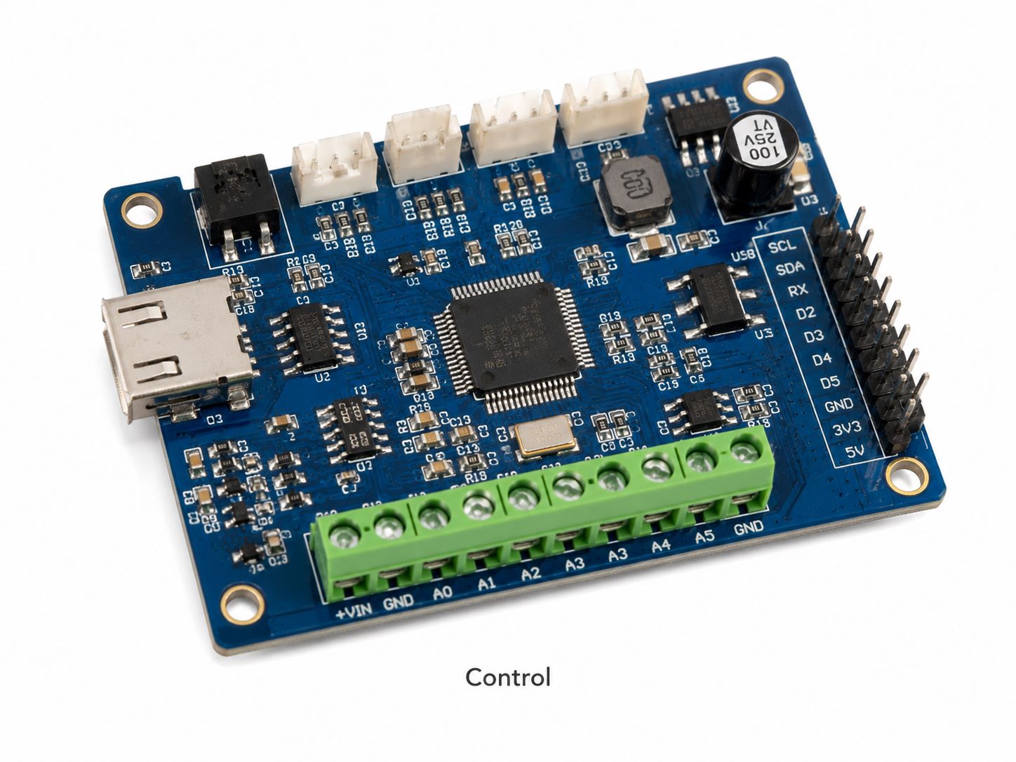
USB 2.0 is still widely used in electronic products because it is simple, stable, and suitable for many basic applications. It is commonly found in charging boards, control boards, debugging interfaces, MCU modules, industrial devices, and low-to-medium-speed data products.
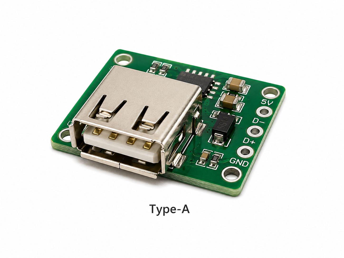
A standard USB 2.0 Type-A or Type-B connector usually has four main pins.
| Pin | Signal | Function | Wire Color |
|---|---|---|---|
| 1 | VBUS | +5V power | Red |
| 2 | D− | Data − | White |
| 3 | D+ | Data + | Green |
| 4 | GND | Ground | Black |
The D+ and D− pins are used as a differential data pair. They should be routed together on the PCB instead of being treated as two unrelated traces. Clean routing helps improve communication stability and reduce avoidable signal problems.
For USB 2.0 PCB layout, the main points are:
- Route D+ and D− as a pair.
- Keep the two traces close and similar in length.
- Avoid long stubs near the USB connector.
- Keep data traces away from noisy power circuits.
- Place ESD protection close to the connector.
- Confirm the connector footprint before PCB fabrication.
- Check the insertion direction and board-edge position.
USB 2.0 is often a practical choice when the product only needs charging, firmware update, basic communication, or debugging. Compared with USB 3.0 and full-featured USB-C designs, it has lower layout complexity and easier assembly control.
Mini USB and Micro USB usually add one more pin, commonly called the ID pin. This pin helps distinguish certain cable or device roles, especially in older portable devices. In many modern designs, Micro USB has been replaced by USB-C, but it is still used in cost-sensitive and legacy products.
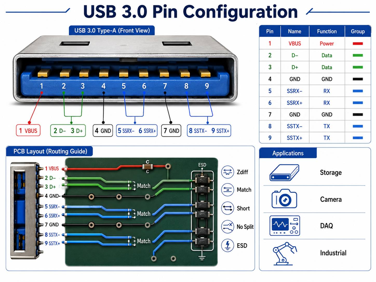
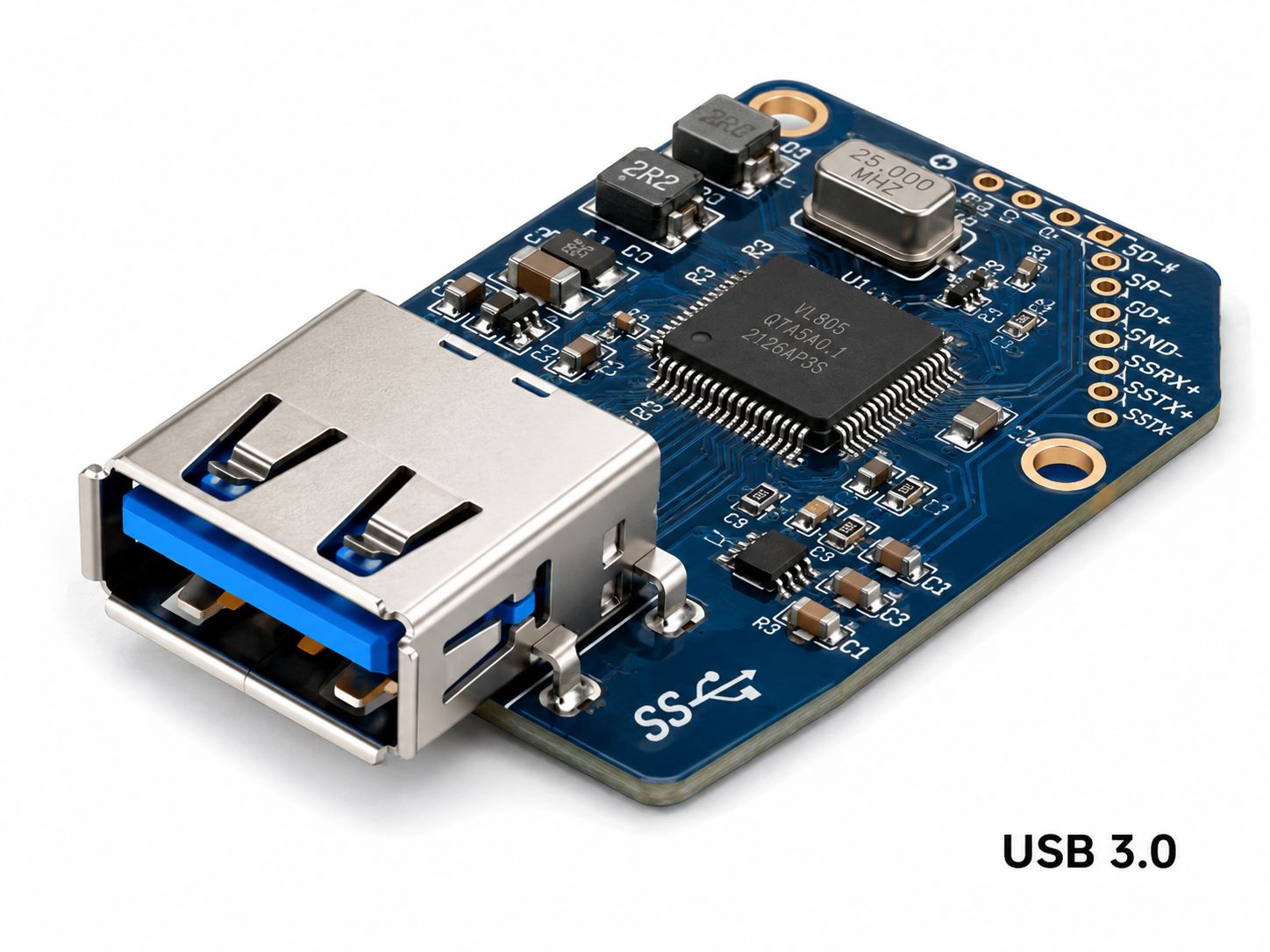
USB 3.0 Pin Configuration
USB 3.0 uses more pins than USB 2.0 because it adds extra signal paths for higher-speed data transfer. It keeps the original USB 2.0 contacts for backward compatibility and adds SuperSpeed transmit and receive pairs.
A typical USB 3.0 Type-A pin configuration includes nine pins.
| Pin | Signal | Function |
|---|---|---|
| 1 | VBUS | Power |
| 2 | D− | USB 2.0 data − |
| 3 | D+ | USB 2.0 data + |
| 4 | GND | Ground |
| 5 | SSRX− | Receive − |
| 6 | SSRX+ | Receive + |
| 7 | GND_DRAIN | Signal ground |
| 8 | SSTX− | Transmit − |
| 9 | SSTX+ | Transmit + |
The key change is the addition of TX and RX differential pairs. These lines carry high-speed signals and require more careful PCB routing. A board may still charge normally through VBUS and GND, but high-speed data can fail if the SuperSpeed pairs are not routed correctly.
For USB 3.0 PCB projects, layout review should focus on:
- Controlled impedance
- Short routing path
- Length matching within each pair
- Stable reference plane
- Reduced via count
- Clean connector breakout
- Separation from switching power circuits
- No routing across plane gaps
- Proper ESD device selection for high-speed lines
USB 3.0 is a better fit when the product needs faster data transfer, such as data acquisition equipment, external storage devices, high-speed modules, test instruments, cameras, and industrial data interfaces.
However, the PCB stack-up and routing quality must support the signal requirement. If the board layout is not suitable, the connector may look correct, but the final product may still show unstable transfer speed, poor enumeration, or intermittent connection.
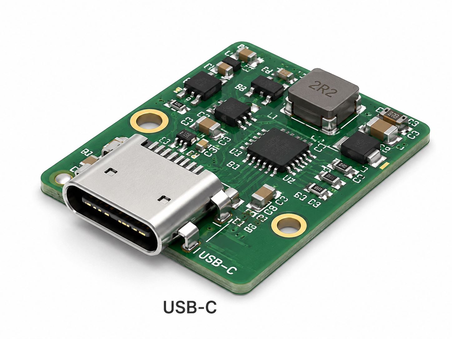
USB-C Pin Configuration
USB-C is a compact and reversible connector with 24 pins. It can support power input, power output, USB 2.0 data, USB 3.x data, Power Delivery, and alternate modes depending on the product design.
However, USB-C should not be understood as one fixed function. A USB-C connector can be used in different ways. Some products use it only for 5V power. Some use it for USB 2.0 data. Some use it for high-speed data. Some use it for Power Delivery. Some use it for video or other alternate modes.
The actual function depends on the circuit, controller, cable, connector, and PCB layout.
| Pin Group | Main Role |
|---|---|
| VBUS | Power path |
| GND | Ground return |
| D+ / D− | USB 2.0 data |
| TX / RX | High-speed data |
| CC1 / CC2 | Cable detection |
| SBU1 / SBU2 | Alternate mode |
| Shield | EMI and strength |
The CC pins are one of the most important differences between USB-C and older USB connectors. They help detect cable insertion, plug orientation, and current capability. Even if the USB-C port is used only as a simple power input, the CC pins still need correct resistor configuration.
USB-C design needs closer checking when the product involves:
- Reversible plug connection
- Higher charging current
- USB Power Delivery
- USB 3.x high-speed data
- DisplayPort or other alternate modes
- Compact PCB space
- Frequent cable insertion
- EMI-sensitive products
- High-current VBUS path
A common mistake is treating USB-C like a simple four-pin connector. It can be used in a simple design, but the required pins must still be handled correctly. Leaving CC pins floating or using the wrong resistor value can stop the port from working as expected.
For PCB manufacturing and assembly, USB-C also requires careful attention to footprint accuracy. USB-C connectors often have fine-pitch pins, shell pads, locating posts, and complex soldering requirements. The land pattern should match the selected manufacturer part number, not just a similar-looking connector.
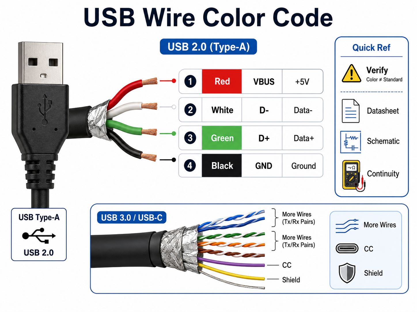
USB Wire Color Code and Pin Mapping
USB wire color code is useful when checking a cable, repairing a simple connection, or wiring a basic USB header. For many USB 2.0 cables, the common color arrangement is red, white, green, and black.
| Color | Signal | Meaning |
|---|---|---|
| Red | VBUS | +5V |
| White | D− | Data − |
| Green | D+ | Data + |
| Black | GND | Ground |
This color code is convenient, but it should not be the only verification method. Some low-cost, customized, or non-standard cables may use different colors. For production work, always confirm the actual connection with the connector datasheet, cable specification, schematic, or continuity test.
Use wire color only as a quick reference when:
- Checking a basic USB 2.0 cable
- Repairing a simple power/data cable
- Identifying VBUS and GND
- Connecting a USB header during early testing
- Comparing cable wiring with a schematic
For USB 3.0 and USB-C cables, the internal structure is more complex. They may include shielded differential pairs, drain wires, CC lines, and additional conductors. In these cases, color alone is not enough. The cable drawing or supplier specification should be checked before assembly or testing.
How to Choose the Right USB Port Pin Layout for a PCB?
Choosing the right USB port pin layout depends on the product function, data speed, power requirement, connector size, and assembly method. The best option is not always the newest connector. It should match the actual product requirement.
| Project Need | Suitable Option |
|---|---|
| Simple 5V input | USB 2.0 or USB-C |
| Basic data | USB 2.0 |
| Faster data | USB 3.0 or USB-C |
| Compact product | Micro USB or USB-C |
| Modern charging port | USB-C |
| Industrial interface | Type-B, Type-A, or USB-C |
| High insertion cycles | Strong mechanical connector |
For PCB projects, the connector choice should consider both electrical and manufacturing factors.
Important selection questions include:
- What current does the USB port need to carry?
- Is data transfer required, or only power input?
- Does the product need USB 2.0 or high-speed data?
- Is USB-C Power Delivery required?
- Is the PCB space limited?
- Will the connector be mounted on the board edge?
- Is the product frequently plugged and unplugged?
- Can the selected connector be assembled reliably?
- Is the connector available from stable suppliers?
- Does the connector footprint match the PCB design rules?
For a simple charging module, a basic USB 2.0 or USB-C power input may be enough. For a high-speed data interface, USB 3.0 or USB-C needs a better PCB stack-up and stricter routing. For small consumer products, USB-C is often preferred because of its size and user-friendly orientation. For industrial equipment, mechanical strength and connector availability may matter more than appearance.
The right USB pin layout should support the product function while remaining practical for PCB fabrication, component sourcing, soldering, inspection, and testing.
How Does USB Port Pin Configuration Affect PCB Layout and Assembly?
USB port pin configuration directly affects PCB layout and assembly quality. A correct schematic is only the first step. The footprint, routing, pad design, soldering process, and inspection method must also match the connector and product function.
Key PCB layout points include:
- Connector footprint: Use the exact datasheet land pattern.
- D+ and D− routing: Keep the pair close and clean.
- USB 3.0 pairs: Control impedance and reduce routing discontinuity.
- USB-C CC pins: Apply the correct connection method.
- VBUS path: Use enough copper width for the target current.
- Ground return: Keep a stable reference path under data traces.
- ESD protection: Place protection devices near the USB port.
- Shield connection: Follow product EMI and grounding needs.
- Board edge design: Check connector position and insertion direction.
- Mechanical pads: Reinforce shell tabs and anchor points.
Assembly-related checks are also important:
- Confirm the connector part number in the BOM.
- Check whether the connector is SMT, through-hole, or hybrid.
- Confirm solder paste opening for fine-pitch pins.
- Review the connector’s heat tolerance for reflow.
- Check whether AOI can inspect the solder joints.
- Confirm if manual inspection is needed for shell tabs.
- Add functional testing when data transfer must be verified.
- Review panelization if connectors are close to the board edge.
Common mistakes include:
- Mirrored USB connector footprint
- Reversed D+ and D− signals
- Wrong USB-C CC resistor design
- ESD device placed too far from the port
- Weak connector soldering
- Poor high-speed routing
- Using a similar but mismatched connector
- VBUS copper width too narrow
- No clear test requirement for USB communication
These problems are easier to correct before production. Once boards are fabricated and assembled, connector-related errors can cause expensive rework or scrap. A careful review before prototype manufacturing can save time and reduce risk.
Need Help With USB Port PCB Manufacturing and Assembly?
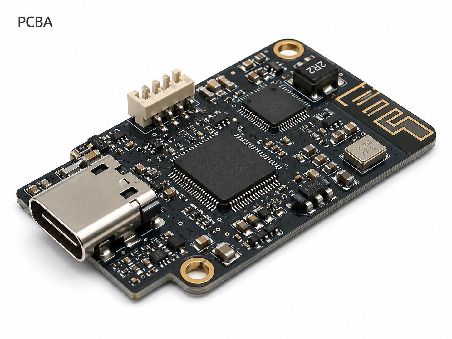
Understanding USB port pin configuration is useful, but reliable production also depends on practical PCB manufacturing and assembly control. Connector footprint accuracy, pad design, solder mask opening, board thickness, surface finish, ESD placement, soldering quality, and testing method can all affect the final USB port performance.
EBest Circuit, also known as Best Technology, supports USB-related PCB projects from prototype to batch production. Our support focuses on PCB layout support within manufacturability requirements, PCB fabrication, component sourcing, SMT assembly, connector soldering, inspection, and functional testing according to customer project needs.
For USB port PCB projects, we can help review production-related details such as:
- Connector footprint
- Pad size
- Solder mask opening
- Surface finish
- Board thickness
- Panel design
- Assembly direction
- BOM and connector part number
- Connector soldering feasibility
- Inspection and testing requirements
We can support different USB connector board projects, including:
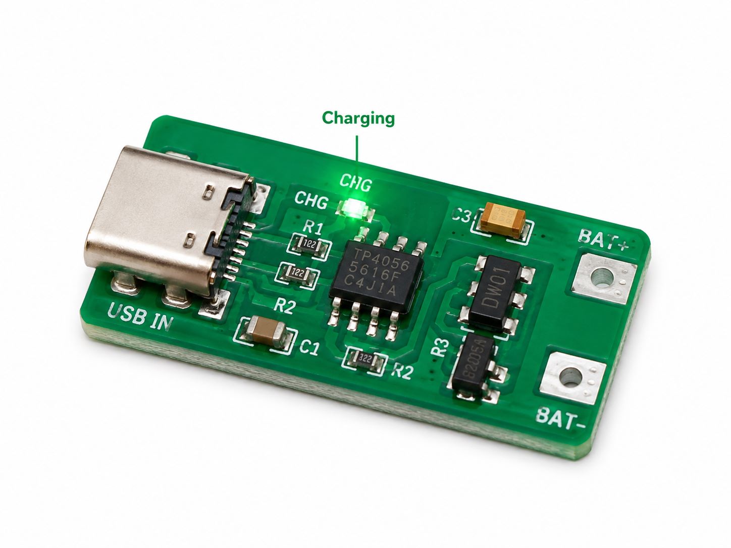
- USB charging boards
- USB interface modules
- Control boards with USB ports
- Industrial USB communication boards
- Consumer electronics PCBAs
- USB Type-A connector boards
- Micro USB PCB assemblies
- USB 3.0 connector boards
- USB-C PCB assemblies
Our service scope is centered on PCB layout support, PCB manufacturing, and PCB assembly. Complete circuit design, product architecture design, firmware development, and system-level electronics design should normally be handled by the customer’s hardware or product design team.
Once your schematic, Gerber files, BOM, pick-and-place file, or assembly drawing is ready, EBest Circuit can help turn the design files into manufacturable PCB and PCBA products. With practical engineering communication and production experience, we help customers reduce avoidable manufacturing issues and move USB PCB projects forward more smoothly. For USB port PCB manufacturing or assembly support, please contact us at sales@bestpcbs.com.
FAQs About USB Port Pin Configuration
How many pins does a USB 2.0 port have?
A standard USB 2.0 Type-A or Type-B port usually has four main pins: VBUS, D−, D+, and GND.
What is the positive pin in a USB port?
VBUS is the positive power pin. In many USB 2.0 cables, it is connected to the red wire and carries +5V.
Which USB pins are used for data?
D+ and D− are used for USB 2.0 data. USB 3.0 adds TX and RX differential pairs for higher-speed transfer.
Are all USB port pinouts the same?
No. USB pinout changes according to connector type and USB generation. USB 2.0, USB 3.0, Micro USB, and USB-C do not use the same full pin structure.
What is the difference between USB pinout and USB pin configuration?
USB pinout usually means the exact pin assignment. USB pin configuration is broader and can include pin position, signal role, connector orientation, PCB footprint, and layout requirements.
Does USB-C always support fast charging?
No. USB-C is a connector type. Fast charging depends on the cable, power source, controller, CC configuration, and power circuit design.
Can USB-C be used only for power?
Yes. USB-C can be used as a power input only, but the CC pins still need the correct resistor configuration for proper detection.
Why does a USB PCB port fail after assembly?
Common causes include wrong connector footprint, reversed signals, weak soldering, poor ESD placement, damaged connector, narrow VBUS trace, or poor data-pair routing.
What files are needed for USB PCB manufacturing and assembly?
Common files include Gerber files, drill files, BOM, pick-and-place file, assembly drawing, connector part number, and testing requirements.
Should USB connectors be tested after assembly?
Yes, if the USB port is used for data or charging performance. Visual inspection can check soldering, but functional testing confirms whether the USB port works as intended.
In summary, the pin configuration of a USB port defines how power, ground, data, high-speed signals, and control pins are arranged inside the connector. USB 2.0 uses a simple four-pin structure. USB 3.0 adds SuperSpeed TX/RX pairs. USB-C uses a 24-pin structure that can support reversible connection, power delivery, high-speed data, and optional alternate modes.
For PCB projects, USB pin configuration should always be checked together with the connector datasheet, schematic, footprint, layout, assembly process, and test plan. A small mistake near the USB connector can lead to charging failure, unstable data transfer, weak soldering, or product reliability problems.
EBest Circuit can support USB port PCB manufacturing and assembly with file review, PCB fabrication, component sourcing, SMT assembly, connector soldering, inspection, and functional testing. With clear design files and production requirements, your USB PCB project can move from prototype to finished PCBA with better manufacturability and fewer avoidable risks. For USB PCB manufacturing or assembly support, pls feel free to contact us at sales@bestpcbs.com.