Board warpage during reflow can reduce SMT yield, damage solder joint reliability and cause final assembly problems. For BGA, fine-pitch ICs, connectors, LED modules, medical electronics and automotive PCBA, even small deformation may lead to solder opens, head-in-pillow defects or housing mismatch.
The best way to control board warpage is to reduce internal stress before PCB fabrication and verify flatness during assembly. This guide explains the causes, design controls, material choices, stackup examples, reflow settings, IPC-TM-650 measurement, bow and twist calculation, and practical repair limits after reflow.
What Is Warpage in PCB?
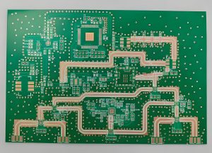
Warpage in PCB means the board is no longer flat. It may bend upward, curve along the length, twist at one corner or deform locally after lamination, baking, solder mask curing, routing or reflow soldering.
Bow means the PCB curves while the four corners stay almost in the same plane. Twist means one corner lifts when the other three corners stay on a flat reference surface. Both problems affect SMT because the PCB surface height becomes uneven during solder paste printing, component placement and soldering.
A board may look flat at room temperature but deform at peak reflow temperature. Therefore, flatness should be checked at important process stages, not only after final delivery.
What Causes Boards to Warp During PCB Manufacturing and Reflow?
Boards warp because copper, laminate, resin, solder mask and mounted components expand and shrink differently under heat. When these forces are not balanced, stress builds inside the PCB and pulls the board out of shape.
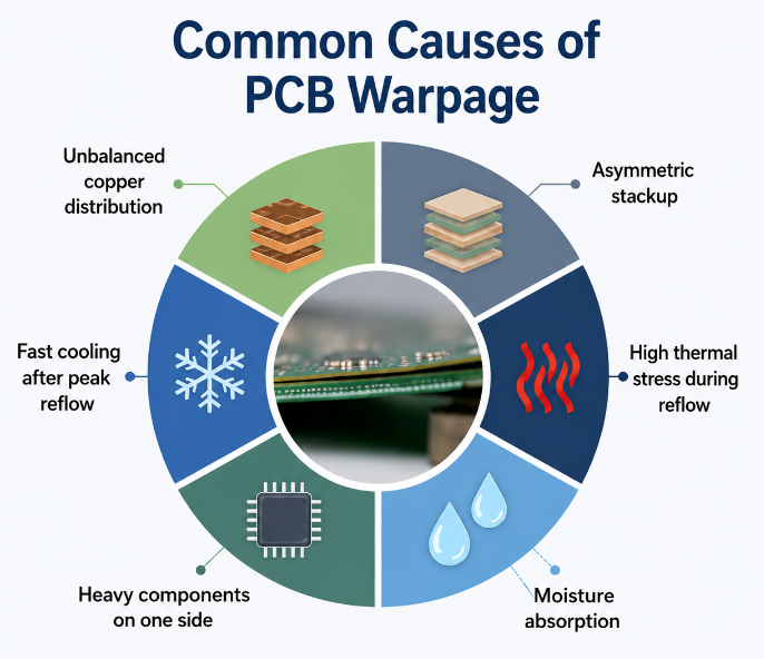
Common causes include:
- Unbalanced copper distribution between top and bottom layers.
- Asymmetric stackup with uneven dielectric thickness.
- High thermal stress during lamination, baking or reflow.
- Large panel size without enough conveyor support.
- Moisture inside laminate before high-temperature exposure.
- Heavy components placed mainly on one side.
- Fast cooling after peak reflow that locks stress into the PCB.
The risk is not only visual bending. Excessive board warpage can cause solder bridges, open joints, BGA cracks and unreliable electrical performance.
Why Does Board Warpage Often Occur With the Length of the Board?
Board warpage often appears along the length because long PCBs have lower stiffness over distance. When heat, copper stress and mechanical support are uneven, the longest unsupported direction usually bends first.
Warpage occurring with the length of the board is common in LED PCBs, power control boards, narrow panels and long industrial control boards. The longer the unsupported span, the easier the PCB can sag, bow or twist during reflow.
This problem becomes worse when the PCB is thin, copper is unbalanced or panel rails are weak. For long boards, better thickness, balanced copper, shorter panel spacing and reflow carriers can greatly reduce deformation risk.
How Does Thermal Stress Cause PCB Deformation During Reflow?
Thermal stress PCB deformation causes come from uneven heating, peak temperature exposure and uneven cooling. During reflow, copper, resin, glass fiber, solder mask and components do not expand at the same rate.
First, the PCB absorbs heat in the preheat and soak zones. Then solder melts near peak temperature, while laminate stiffness drops. If the top and bottom sides expand differently, the board starts to bend. During cooling, the structure contracts again, but part of the deformation may remain.
A stable reflow profile reduces sudden temperature differences across the PCB. This is especially important for thick copper PCB, large panels, heavy assemblies and boards with BGA or fine-pitch packages.
How Does Coefficient of Thermal Expansion Affect PCB Warpage?
Coefficient of thermal expansion affects PCB warpage because every material inside the PCB expands and shrinks at a different rate during heating and cooling. Copper, FR-4 laminate, prepreg, solder mask, component packages and adhesives do not move in exactly the same way under reflow temperature.
When the PCB enters the reflow oven, copper planes heat up quickly, while laminate and resin respond differently. If the top and bottom sides of the PCB have similar copper coverage and dielectric structure, the expansion force is more balanced. As a result, the board can stay flatter through the heating and cooling process.
However, if one side has more copper, thicker material or stronger restraint, the PCB may bend toward one direction. This is a common reason for coefficient of thermal expansion PCB warpage in SMT production. The higher the material mismatch and structural imbalance, the greater the risk of bow or twist after reflow.
CTE mismatch is more serious in BGA assemblies, heavy copper PCB, rigid-flex PCB and long PCB designs. These products usually have tighter flatness requirements because small deformation can affect solder joint quality, component coplanarity and mechanical assembly fit.
To reduce this risk, engineers should choose stable laminate, control resin content, balance copper layers and keep the stackup symmetrical. The key point is to make both sides of the PCB expand and contract as evenly as possible during reflow. This helps reduce board warpage and improves SMT assembly reliability.
What Design Factors Help Reduce PCB Board Warpage Before Fabrication?
Good design reduces stress before the PCB enters production. Warpage control should start during layout and DFM review, not after SMT defects appear.
Key design actions include:
- Balance copper on opposite layers to reduce uneven expansion.
- Use symmetrical stackup whenever the electrical design allows it.
- Avoid large copper-free areas on only one side of the PCB.
- Increase board thickness for long, thin or heavy assemblies.
- Add panel rails and support tabs for weak outlines.
- Distribute heavy components evenly instead of loading one side.
- Review slots, cutouts and irregular shapes because they reduce stiffness.
For high-risk products, DFM review should include flatness risk, not only trace width, spacing and hole size.
What Material Choices Help Prevent Board Warpage?
Material choice affects board warpage because PCB laminate must keep enough stiffness during lamination, baking and reflow. If the material softens too much or absorbs moisture, the board can bend after heating and cooling. The right material should match reflow temperature, board size, copper weight and final assembly stress.
- Use high-Tg FR-4 for better reflow stability.
High-Tg laminate keeps stronger mechanical stability at high temperature. It helps reduce softening during peak reflow and lowers the risk of permanent deformation after SMT assembly. - Choose low-CTE material for high-reliability PCB.
Lower CTE helps the PCB expand less during heating. This is useful for BGA, fine-pitch SMT, automotive electronics, medical devices and other products with strict flatness requirements. - Match laminate strength with copper weight.
Heavy copper PCB creates more thermal and mechanical stress than standard copper PCB. If the laminate is not strong enough, board warpage may appear after lamination or reflow. - Control moisture before reflow.
Moisture inside the laminate can expand quickly during heating. Proper storage and baking help reduce internal pressure, delamination risk and PCB board warpage. - Select suitable material for long or thin boards.
Long LED PCB, narrow control boards and thin panels need better stiffness. Increasing material thickness or using stronger laminate can reduce bending along the board length. - Review rigid-flex material combinations carefully.
In rigid-flex PCB, PI film, FR-4, adhesive and stiffener materials expand differently. Poor material matching can create local bending near the rigid-flex transition area.
The material rule is simple: use reflow-stable laminate, reduce CTE mismatch, control moisture and match material strength with PCB structure. Good material selection gives the stackup a stable base before copper balance and layer symmetry are reviewed.
What Stackup Choices Help Prevent Board Warpage?
Stackup design controls how stress is distributed through the PCB thickness. Even with good laminate, an unbalanced stackup can still cause board warpage during reflow. A stable stackup should keep copper weight, dielectric thickness and layer structure balanced from the centerline outward.
- Keep the stackup symmetrical.
The top half and bottom half of the PCB should be similar in copper weight and dielectric structure. Symmetry helps both sides expand and shrink evenly during heating and cooling. - Balance copper between outer layers.
Avoid large copper areas on only one side of the PCB. If L1 has heavy copper but L4 has sparse routing, the board may bend toward one side during reflow. - Balance inner plane layers.
Ground and power planes should be arranged close to the centerline when possible. This reduces uneven stress and helps maintain flatness after lamination. - Avoid large dielectric thickness differences.
If one side uses thin prepreg and the other side uses thick prepreg, the PCB may shrink unevenly after lamination. Core and prepreg thickness should stay as even as the design allows. - Add copper balance in empty areas.
Copper thieving or copper balancing patterns can help reduce stress in sparse areas. This is useful when one layer has large copper pours and another layer has open space. - Increase thickness for long or narrow PCB.
Long boards are more likely to bend along the length. For high-risk designs, increasing thickness from 1.0 mm to 1.6 mm or 2.0 mm can improve stiffness and reduce deformation.
A good 4-layer stackup should keep copper and dielectric structure balanced around the centerline.
| Layer | Balanced 4-Layer Stackup Example |
|---|---|
| L1 | Signal + copper balance |
| Prepreg | 0.20 mm |
| L2 | Ground plane |
| Core | 0.80 mm |
| L3 | Power plane |
| Prepreg | 0.20 mm |
| L4 | Signal + copper balance |
In this example, L1 and L4 are balanced outer layers, while L2 and L3 are inner plane layers near the centerline. The prepreg thickness on both sides is similar, so the PCB expands and cools more evenly during reflow. This structure is suitable for SMT boards that need better flatness.
For stable SMT production, the stackup rule is clear: keep copper balanced, keep dielectric thickness symmetrical and review warpage risk during DFM before PCB fabrication.
How Should Reflow Profile Settings Be Controlled to Reduce Board Warpage?
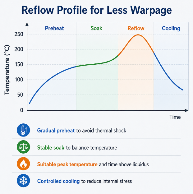
Reflow profile settings should be controlled to heat the PCB evenly, reduce thermal shock and avoid unnecessary peak temperature exposure. The goal is not to make the oven hotter, but to let the whole PCB reach soldering temperature in a stable and balanced way.
- Use a gradual preheat stage.
The PCB should not enter a sharp temperature rise too quickly. A smooth preheat helps copper, laminate, solder mask and components warm up together, reducing sudden thermal stress. - Keep the soak zone stable.
The soak zone helps balance temperature across large copper areas, heavy components and different PCB regions. This is important for thick PCB, heavy copper PCB and boards with uneven component density. - Avoid excessive peak temperature.
Peak temperature must be high enough for solder wetting, but it should not be much higher than the solder paste requirement. Excessive peak heat can soften the laminate and increase board warpage. - Control time above liquidus.
The solder must stay molten long enough to form reliable joints, but too much time above liquidus increases thermal exposure. Long exposure can add stress to the PCB and components. - Use slower and controlled cooling.
Very fast cooling can lock internal stress into the PCB. A controlled cooling stage helps the board contract more evenly and reduces the risk of permanent deformation. - Measure temperature at different PCB locations.
Thermocouples should be placed near dense components, large copper areas, board edges and the center area. This helps confirm whether the entire PCB heats evenly during reflow. - Create separate profiles for high-risk boards.
Long PCB, thin PCB, BGA assemblies, heavy copper PCB and rigid-flex PCB should not automatically use the same profile as standard boards. A custom profile can reduce deformation risk. - Check board flatness after profile validation.
A profile is not fully proven only because solder joints look good. The PCB should also be checked for bow and twist after reflow, especially when the project has strict SMT flatness requirements.
For stable SMT production, the reflow profile rule is clear: use gradual heating, balanced soaking, suitable peak temperature, controlled cooling and real PCB temperature measurement. This helps reduce board warpage while keeping solder joint quality reliable.
How Do Fixtures, Carriers and Panel Support Help Reduce Board Warpage?
Fixtures, carriers and panel support reduce mechanical sag while the PCB is soft at high temperature. They are especially useful for thin boards, long boards, heavy assemblies and irregular outlines.
Effective support methods include:
- Reflow carriers to hold thin or flexible PCBs flat through the oven.
- Edge rails to improve conveyor stability.
- Center support pins for wide panels.
- Balanced panelization to avoid uneven stress after routing.
- Selective pressure fixtures where local bending is predictable.
- Controlled depaneling to prevent stress release after assembly.
The proper way to glue boards together for less warpage is not random adhesive bonding. If bonding is required, adhesive type, cure temperature, pressure and copper balance must be engineered together.
What Are PCB Warpage Limits for SMT and PCBA Production?
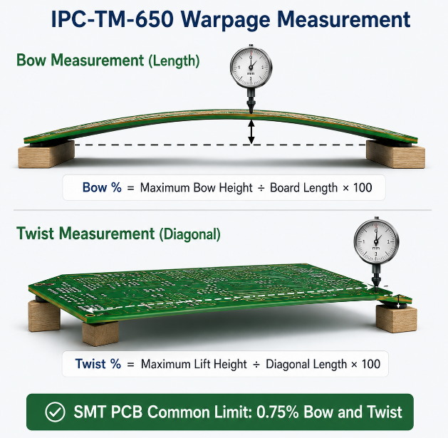
PCB warpage allowance depends on product class, assembly type, board size and customer specification. In common IPC-related practice, printed boards using surface mount components are often controlled to 0.75% maximum bow and twist, while other boards may allow 1.5%.
| Item | Typical Limit | Production Note |
|---|---|---|
| SMT PCB | 0.75% | Common IPC-related target |
| Non-SMT PCB | 1.5% | Less strict assembly condition |
| BGA Assembly | 0.50% or tighter | Often customer-specific |
| Fine-Pitch PCBA | 0.50% or tighter | Needed for placement accuracy |
| Long LED PCB | Custom limit | Depends on fixture and housing |
| Rigid-Flex PCB | AABUS | Based on design agreement |
For strict SMT projects, PCB warpage limits IPC standard language should be confirmed on the drawing, purchase order and quality agreement. This avoids disputes between PCB fabrication, SMT assembly and final product inspection.
How to Check PCB Warpage by IPC-TM-650 Measurement?
IPC-TM-650 measurement checks PCB bow and twist by comparing the board surface with a flat reference plane. The goal is to measure the real gap without pressing, bending or forcing the PCB into a flat condition.
Step 1: Prepare a flat inspection surface.
Use a clean, calibrated flat plate or inspection table. Dust, solder residue or uneven support can affect the measurement result, so the surface should be checked before placing the PCB.
Step 2: Let the PCB return to room temperature.
The board should be measured after cooling unless the project requires high-temperature warpage testing. Measuring too soon after reflow may give unstable results because the PCB is still releasing thermal stress.
Step 3: Place the PCB naturally on the flat surface.
Put the board on the reference plane without pressing it down. If the PCB is forced flat by hand, the real board warpage condition will be hidden and the result will not be reliable.
Step 4: Check bow deformation.
For bow measurement, find the highest gap between the PCB and the flat surface along the board length or width. This gap is used to calculate the bow percentage.
Step 5: Check twist deformation.
For twist measurement, keep three corners touching the flat surface and measure the lifted corner or the highest diagonal gap. This shows how much the PCB twists out of plane.
Step 6: Record the board size and maximum gap.
Measure the board length, width or diagonal according to the calculation method. Then record the maximum bow height or twist height clearly for quality review.
Step 7: Calculate bow and twist percentage.
Convert the measured height into a percentage using the PCB bow and twist calculation formula. This makes the result easier to compare with the PCB warpage allowance or customer drawing.
Step 8: Compare the result with the required limit.
For SMT production, many projects use 0.75% maximum bow and twist as a common reference. For BGA, fine-pitch PCBA or strict mechanical assemblies, the limit may be tighter.
Step 9: Keep inspection records for traceability.
Record the measured value, inspection stage, board lot, panel direction and operator information. These records help identify whether board warpage comes from PCB fabrication, reflow profile, fixture support or assembly handling.
For accurate IPC-TM-650 warpage measurement, the key rule is simple: measure the PCB in its natural state, use a flat reference surface, record the maximum gap and compare the calculated percentage with the required SMT or customer limit.
How to Calculate PCB Bow and Twist for Warpage Evaluation?
The PCB bow and twist calculation formula converts deformation height into a percentage. This makes it easier to compare different board sizes and judge whether the board meets the required PCB warpage specification for SMT.
For bow, the common calculation is:
Bow % = Maximum Bow Height ÷ Board Length × 100
For twist, the common calculation is:
Twist % = Maximum Lift Height ÷ Diagonal Length × 100
For example, if a 200 mm PCB has a 1.0 mm bow height, the bow value is 0.50%. If a board diagonal is 250 mm and one corner lifts 1.5 mm, the twist value is 0.60%.
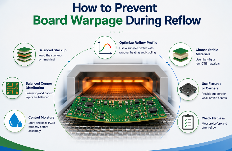
How to Prevent Board Warpage During Reflow?
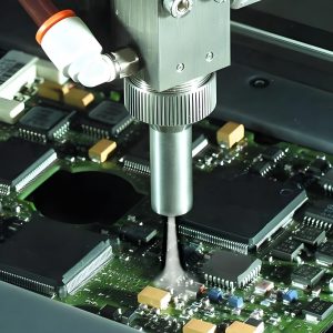
Preventing board warpage during reflow should start before SMT assembly. Once the PCB is already bent after soldering, repair options are limited. The best method is to reduce structural stress, moisture stress and thermal stress before the board enters the reflow oven.
- Balance copper distribution.
Large copper areas should not stay only on one side of the PCB. If top and bottom copper coverage is very different, both sides will expand unevenly during heating and may cause bow or twist. - Use a symmetrical stackup.
Copper weight, prepreg thickness and core thickness should be balanced from the centerline outward. A symmetrical stackup helps both sides of the PCB release stress evenly during reflow. - Choose stable laminate material.
High-Tg FR-4 or low-CTE material is better for thin PCB, long PCB, heavy copper PCB, BGA assembly and fine-pitch SMT. Stable material helps reduce softening at peak reflow temperature. - Control moisture before assembly.
Moisture inside the PCB may expand quickly in the oven and increase board warpage risk. Dry storage and proper baking help reduce deformation, blistering and delamination. - Optimize the reflow profile.
Use gradual preheating, stable soaking, suitable peak temperature and controlled cooling. Excessive peak heat or fast cooling can increase thermal stress and cause permanent deformation. - Use fixtures or carriers for weak boards.
Thin PCB, long PCB, rigid-flex PCB and irregular panels may sag during reflow. Reflow carriers, edge rails or center supports can keep the board stable through the oven. - Check flatness before and after reflow.
Measure bow and twist before SMT and after reflow for high-risk boards. This helps confirm whether the issue comes from PCB fabrication, storage, reflow profile or fixture support.
For stable production, the rule is clear: balance the PCB structure, select stable material, control moisture, optimize reflow and support weak panels during heating.
How to Fix Warped Circuit Board After Reflow?
A warped circuit board after reflow should be treated as a reliability risk, not only a shape problem. The correct approach is to measure the deformation first, inspect solder reliability and then decide whether repair, fixture support or remake is suitable.
- Let the board cool before inspection.
Do not judge the PCB immediately after it leaves the oven. Let it return to room temperature first, because the board may still be releasing thermal stress. - Measure bow and twist first.
Place the PCB naturally on a flat reference surface and measure the maximum gap. Then compare the result with the PCB warpage allowance, SMT requirement or customer drawing. - Inspect sensitive solder areas.
Check BGA, QFN, fine-pitch ICs, connectors and heavy components carefully. For hidden solder joints, X-ray inspection may be needed to confirm reliability. - Avoid manual straightening.
Do not bend the PCB back by hand. Uncontrolled force may crack vias, damage inner traces, lift pads or weaken solder joints, even if the board looks flatter. - Use controlled baking only in limited cases.
If the deformation is related to moisture or temporary stress, controlled baking with flat support may help. This should be done only when the material and components can tolerate the temperature. - Use fixture support only when warpage is slight.
If the board is still within the allowed limit, a fixture or carrier may help it pass the next process. However, solder joint inspection and mechanical fit must still be confirmed. - Remake boards with serious deformation.
If the PCB exceeds flatness limits, affects BGA reliability or cannot fit the housing, remaking the board is safer than forced repair. - Correct the root cause before mass production.
Repeated warpage should be traced to copper balance, stackup symmetry, material selection, moisture control, reflow profile or fixture support.
For warped boards after reflow, the key rule is simple: measure first, inspect solder joints, avoid forced straightening and correct the process cause before continuing production.
FAQs About PCB Board Warpage
Q1: Is PCB board warpage always caused by reflow?
A1: No. PCB board warpage can happen before reflow due to unbalanced copper, asymmetric stackup, poor material selection, moisture absorption or stress from lamination. Reflow may only make the existing stress more visible. The real cause should be checked from PCB fabrication, storage and SMT assembly together.
Q2: What is the most common cause of PCB board warpage?
A2: The most common cause is structural imbalance. If copper coverage, dielectric thickness or material stress is different between the top and bottom sides, the PCB may bend during heating and cooling. Unbalanced copper and asymmetric stackup are the first items to check during DFM review.
Q3: Can PCB board warpage affect solder paste printing?
A3: Yes. If the PCB surface is not flat, the stencil may not contact the board evenly. This can cause too much solder paste in one area and insufficient paste in another area. For fine-pitch SMT and BGA assembly, even small height differences can create solder defects.
Q4: Why is PCB board warpage serious for BGA assembly?
A4: BGA solder joints are hidden under the package, so warpage can create open joints, head-in-pillow defects or cracked solder balls without obvious visual signs. BGA assemblies usually need tighter flatness control than standard SMT boards, especially after reflow.
Q5: Can thicker PCB reduce PCB board warpage?
A5: Thicker PCB can improve stiffness and reduce bending, especially for long or narrow boards. However, thickness alone cannot solve the problem if copper is unbalanced or the stackup is asymmetric. Thickness works best with balanced copper, stable material and proper reflow support.
Q6: Should PCBs be baked before reflow to reduce warpage?
A6: Baking can help when moisture absorption is a risk, especially for long-stored PCBs or moisture-sensitive materials. However, baking cannot fix poor stackup or copper imbalance. Baking should be used as moisture control, not as the main solution for structural warpage.
Q7: What flatness limit should buyers specify for SMT PCB?
A7: Many SMT projects use 0.75% maximum bow and twist as a common reference. However, BGA, fine-pitch components, connectors and strict mechanical assemblies may require 0.50% or tighter. The final requirement should be written clearly on the drawing or quality agreement.
Q8: Can PCB board warpage be accepted if the board still works electrically?
A8: Not always. A warped PCB may pass a simple electrical test but still have hidden solder stress, weak BGA joints or mechanical fit problems. Electrical function does not always prove long-term reliability, especially for automotive, medical and industrial PCBA.
Q9: How can suppliers prevent PCB board warpage in mass production?
A9: Suppliers should review stackup symmetry, copper balance, laminate selection, panel design, storage control, reflow profile and fixture support before mass production. They should also measure bow and twist on high-risk boards. Process control is more reliable than post-reflow repair.
Q10: Does panelization affect PCB board warpage?
A10: Yes. Weak rails, large open areas, poor tab placement and long unsupported spans can make panels bend during SMT. Good panelization should support the PCB through printing, placement, reflow and depaneling. This is especially important for thin, long or irregular PCBs.
Q11: Can warped circuit boards be repaired after reflow?
A11: Slight deformation may be reviewed and controlled with fixture support or limited baking in some cases. Serious warpage is difficult to repair safely because forced bending may damage vias, traces or solder joints. Boards that exceed flatness limits often need remake instead of repair.
Q12: What information should buyers send to a PCB supplier to control warpage?
A12: Buyers should send Gerber files, stackup, board thickness, copper weight, material requirement, component layout, reflow condition and flatness limit. For BGA or high-reliability PCBA, they should also provide inspection requirements. Clear requirements help the supplier control PCB board warpage before production.
Conclusion
Board warpage is not only a PCB flatness issue. It can affect solder paste printing, component placement, BGA reliability and final PCBA assembly quality. Balanced copper, symmetrical stackup, stable material, controlled reflow and proper fixture support are the key points for reducing board warpage during production.
If your project involves BGA, fine-pitch SMT, long PCB, rigid-flex PCB or high-reliability electronics, early DFM review can help reduce warpage risk before mass production. EBest Circuit provides PCB fabrication, PCBA assembly, reflow profile control, X-ray inspection and quality testing for custom OEM/ODM projects. Send your Gerber files, BOM and assembly requirements to sales@bestpcbs.com for a PCBA quotation.