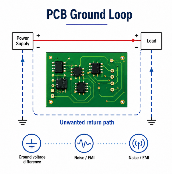
A PCB ground loop happens when ground current can return through more than one unintended path. It can create noise, EMI, unstable sensor readings, audio hum, communication errors and RF performance loss. The real issue is not that a PCB has ground copper. The issue is that return current flows through a path the designer did not control.
In PCB design, grounding should be planned from the schematic, stack-up, layout, cable connection and final enclosure. A board may look correct in CAD but still fail after cables, chassis, shields or external power supplies are connected. This guide explains how ground loops form on a PCB, what a bad layout looks like, how to test the problem and how to avoid it before production.
What Is a Ground Loop in PCB?
A PCB ground loop is an unwanted closed path that allows ground current to circulate through more than one route. The core problem is uncontrolled return current, not the ground connection itself.
In a simple circuit, current leaves the power source and returns through ground. In a real PCB, the return path is affected by trace position, plane continuity, cable shields, chassis contact, connectors and power loads. When these paths form a loop, noise current may flow through sensitive areas.
This is why a ground loop in PCB design is often linked to analog errors, EMI, RF noise and unstable system behavior. In practical troubleshooting, the question is not only whether all grounds are connected, but whether the return current follows the intended path.
How Do Ground Loops Form on a PCB?
Ground loops form on a PCB when two or more ground paths connect the same reference points at different locations. Once current can return through several routes, voltage difference may appear between ground points.
This often happens when power ground, signal ground, shield ground and chassis ground are connected without a clear strategy. Long ground traces, split planes, multiple cable shields and metal standoffs can also create hidden loops.
In many projects, ground loops in PCB layouts are not obvious during schematic review. They appear after assembly, testing or enclosure installation because the full current path includes the whole product, not only the bare board.
Why Are PCB Ground Loops a Problem for Noise and EMI?
PCB ground loops create noise because every ground path has resistance and inductance. When current flows through that impedance, the ground reference is no longer stable.
For analog circuits, this can shift sensor signals or ADC readings. For digital circuits, it can cause jitter, false triggering, reset problems or communication errors. For switching power circuits, it can increase conducted and radiated EMI.
A large loop can also behave like an antenna. It may receive external electromagnetic noise or radiate switching noise from the PCB. Therefore, a PCB ground loop is both a signal integrity problem and an EMI control problem.
| Problem | Cause | Result |
|---|---|---|
| Analog noise | Shared ground impedance | Sensor error |
| EMI failure | Large loop area | Radiation risk |
| Audio hum | Multiple ground references | 50/60 Hz noise |
| RF instability | Poor return path | Signal loss |
| Logic error | Ground bounce | False switching |
What Are the Common Symptoms of a PCB Ground Loop?
A PCB ground loop often appears as a noise problem that changes when cables, power supplies, probes or the enclosure are connected. The key sign is that the fault is not stable under different grounding conditions.
Common symptoms include:
- Analog signal drift: Sensor readings, ADC values or reference voltages move when motors, relays, heaters or switching regulators operate.
- Audio hum or low-frequency noise: Audio circuits may show 50/60 Hz hum when external equipment, shields or grounded power supplies are connected.
- Random reset or logic error: Microcontrollers, digital ICs or communication modules may reset or misread signals when ground voltage shifts during load changes.
- Communication instability: CAN, RS-485, UART, USB, Ethernet or sensor buses may show packet loss, CRC errors or intermittent connection failure.
- EMI test failure: A large loop area may radiate switching noise or pick up external interference, causing conducted or radiated EMI issues.
- RF sensitivity loss: Wireless modules may lose range, suffer antenna detuning or show poor signal quality when ground current enters the RF area.
- Probe-dependent measurement: The waveform may change when an oscilloscope ground clip, PC cable or debug tool is attached.
These symptoms do not prove a PCB ground loop by themselves. However, if the issue changes after modifying a cable, shield, chassis bond or external ground path, the return-current path should be checked first.
What Is a Common Ground Loop PCB Example?
A common ground loop PCB example is a mixed-signal control board that uses one area for sensors and another area for a motor driver. The problem starts when analog return current and high-current load return share the same ground path.
A typical case looks like this:
- Project background: The PCB has a temperature sensor, ADC input, microcontroller, motor driver and external power connector.
- Wrong layout condition: The sensor ground returns through the same narrow ground trace used by the motor driver current.
- What happens during operation: When the motor starts, load current creates voltage drop on the shared ground path.
- Observed fault: The ADC value shifts, the temperature reading jumps, or the control system makes wrong decisions.
- Why it is a ground loop problem: The ground reference at the sensor is no longer the same as the ground reference at the controller.
Another example is a PCB connected to a PC through USB while also connected to a grounded power adapter. The USB shield, signal ground and power ground may create an external loop. The board may work alone, but noise appears after the USB cable and power adapter are connected together.
A better design separates high-current return paths from sensitive analog return paths, keeps the ground plane continuous, controls the shield connection and reviews the full cable system before production.
What Does a Bad PCB Ground Loop Layout Look Like?
A bad PCB ground loop layout usually has long ground traces, broken planes, uncontrolled ground bridges and sensitive circuits placed in noisy return paths. The layout may still pass netlist checking because the electrical connection exists, but the return path is poor.
Common bad layout signs include:
- Ground routed as a thin trace instead of a low-impedance plane
- Signal traces crossing ground plane gaps
- Switching current returning through analog ground
- Split ground planes connected at multiple distant points
- Cable shield tied to signal ground without a chassis plan
- Test points or connectors creating extra ground routes
A bad example PCB for ground loops often looks electrically connected but performs poorly under real load. During review, engineers should trace both the signal path and the return path, especially around connectors, regulators, motors, relays and analog inputs.
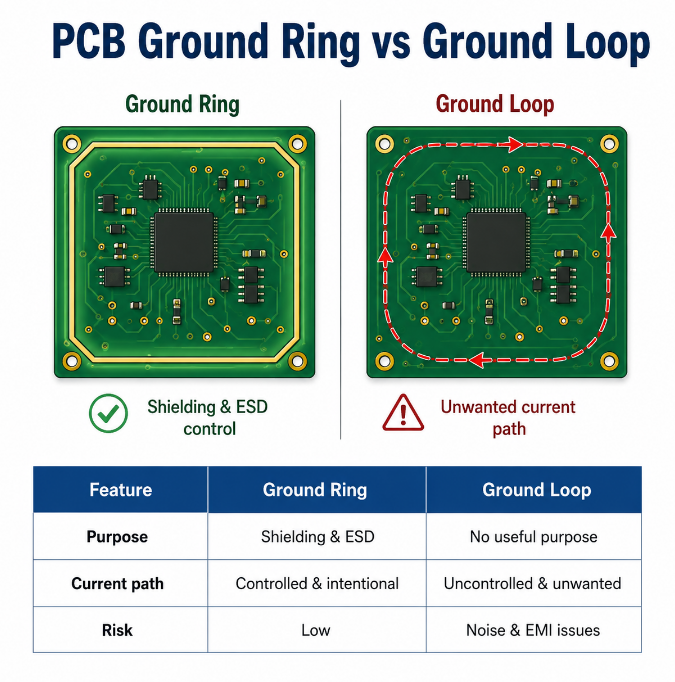
What Is the Difference Between PCB Ground Ring and Ground Loop?
A PCB ground ring is a designed copper structure. A ground loop is an unwanted current path. The main difference is whether the current path is intentional, controlled and useful.
| Item | PCB Ground Ring | PCB Ground Loop |
|---|---|---|
| Definition | Planned copper ring connected to ground | Unwanted closed ground-current path |
| Purpose | Shielding, guarding, ESD control or chassis bonding | No design purpose |
| Current control | Current path is defined by design | Current path is uncontrolled |
| Typical location | Board edge, RF area, analog input, high-impedance node | Around cables, planes, connectors or chassis |
| Main benefit | Reduces noise pickup or improves shielding | No benefit in normal design |
| Main risk | Wrong connection point may carry noisy current | Causes noise, EMI or ground offset |
| RF impact | Can improve shielding if designed correctly | Can detune antenna or increase RF noise |
| Analog impact | Can protect sensitive nodes as a guard ring | Can shift sensor or ADC reference |
| Design rule | Connect with a clear grounding strategy | Remove or control the loop path |
| Review focus | Tie point, current type, nearby signals | Loop area, shared impedance, external paths |
A PCB ground ring is not automatically a problem. It becomes risky when it connects to ground at multiple uncontrolled points or carries return current from noisy circuits. In contrast, a PCB ground loop should be identified and corrected because it creates an unstable reference path.
How Do Ground Planes Affect Ground Loops in PCB Design?
Ground planes help reduce ground impedance and keep return current close to the signal path. A continuous ground plane is usually safer than long routed ground traces.
However, ground planes do not automatically remove every loop risk. Slots, split planes, copper islands, poor via placement and connector gaps can force return current to detour. This increases loop area and EMI risk.
Ground plane loop problems in PCB design often happen when designers split copper without understanding return current. For most multilayer PCB designs, one solid reference plane with smart component placement is more reliable than several small ground islands.
Should You Use Single-Point Grounding or Multi-Point Grounding in PCB Design?
Single-point grounding and multi-point grounding are both valid, but they fit different conditions. The correct choice depends on frequency, current level, circuit sensitivity and system grounding.
Single-point grounding is often useful for low-frequency analog and sensor circuits because it prevents heavy current from flowing through a sensitive reference. The risk is that long return paths may create high impedance at higher frequencies.
Multi-point grounding is common in high-speed digital, RF and chassis-shielded systems. It keeps high-frequency return paths short, but it must be planned carefully. In many modern PCB designs, a solid ground plane with controlled placement is the best practical choice.
| Method | Best Use | Risk |
|---|---|---|
| Single-point | Low-frequency analog | Long return path |
| Multi-point | High-speed or RF | Circulating current |
| Hybrid | Mixed systems | Poor planning |
| Solid plane | Compact PCB design | Plane cuts |
How Should Analog Ground and Digital Ground Be Handled in Mixed-Signal PCB Design?
Analog ground and digital ground should be handled by placement and return-current control, not by random copper splitting. The goal is to keep noisy current away from sensitive analog reference paths.
Practical rules include:
- Place analog and digital circuits in clear zones: Keep ADC inputs, sensors, amplifiers and references away from clocks, switching regulators, relays and fast buses.
- Use one continuous ground plane when possible: A solid plane usually gives a shorter and lower-impedance return path than separated ground islands.
- Do not route signals across ground splits: When a trace crosses a split, its return current must detour, increasing loop area and EMI risk.
- Connect split grounds at a controlled point if splitting is required: The connection is often placed near the ADC, DAC or mixed-signal IC reference point.
- Keep digital return current out of analog areas: Fast digital traces should stay over the digital section of the reference plane.
- Place decoupling close to each IC: The capacitor, power pin and ground connection should form a very small loop.
- Separate noisy power circuits physically: Switching regulators, motor drivers and high-current loads should not return through analog sensor ground.
- Review the full system connection: Cable shields, chassis ground and external power supplies can defeat a clean mixed-signal layout if they are not planned.
A good mixed-signal layout does not rely on labels such as AGND and DGND alone. It controls where current flows.
How to Avoid Ground Loops in PCB Layout?
To avoid ground loops in PCB layout, define the return path before routing is finished. Every signal, power load, shield and connector should have a predictable ground return route.
Use these layout practices:
- Use a continuous ground plane: A solid reference plane reduces impedance and keeps return current close to the signal trace.
- Keep high-current loops small: Power input, switching regulator, motor driver and relay current paths should be short and compact.
- Avoid broken ground under critical traces: Do not route clocks, RF traces, ADC inputs or high-speed lines over slots, gaps or split planes.
- Separate noisy and sensitive circuits: Place switching power, motors and digital buses away from sensors, amplifiers and analog references.
- Control cable shield grounding: Decide whether the shield connects to chassis ground, signal ground or both through controlled components.
- Use stitching vias correctly: Add ground vias near layer transitions, connector shields, board edges and RF zones to reduce return-path detours.
- Avoid isolated copper islands: Floating copper can pick up noise and does not provide a reliable return path.
- Review connector pinout early: Poor ground pin placement can force current across the PCB and create large loop areas.
- Add useful test points: Ground test points near power input, analog reference, switching power and chassis help later troubleshooting.
- Check the layout under real current flow: Do not rely only on net names. Follow the actual path from source to load and back to ground.
These PCB grounding techniques for noise reduction help prevent hidden loops before prototype, EMC testing and mass production.
How Do Connectors, Cables and Chassis Ground Create PCB Ground Loops?
Connectors, cables and chassis ground create PCB ground loops when they add external return paths. Many loop problems do not exist on the bare PCB; they appear after the system is fully connected.
For example, a board may connect to a PC, power adapter, sensor cable and metal enclosure at the same time. Each connection may carry shield, earth or signal ground. If those grounds connect at different points, circulating current may flow.
This is common in industrial control, medical equipment, audio devices, RF modules and long-cable systems. The PCB layout should be reviewed together with cable shielding, connector pinout, chassis bonding and power supply grounding.
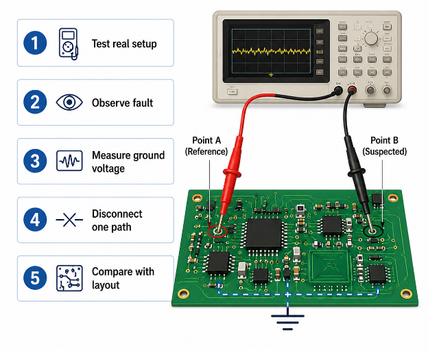
How to Test and Identify a Ground Loop Problem in PCB?
Testing should reproduce the real failure condition. A PCB ground loop is often invisible during bare-board checking but visible during system-level operation.
Step 1: Test the PCB in its real setup.
Connect the normal power supply, load, communication cable, sensor cable, shield and enclosure. Many ground loop problems only appear after the full system is connected.
Step 2: Observe when the fault appears.
Check whether the noise happens during motor start, relay switching, RF transmission, USB connection, charger connection or enclosure contact. This helps narrow down the current path.
Step 3: Measure ground voltage difference.
Use a multimeter or oscilloscope to measure voltage between suspected ground points while the system is operating. A changing ground voltage may show shared impedance or loop current.
Step 4: Use proper oscilloscope probing.
Use a short ground spring or differential probe when possible. A long oscilloscope ground lead can create another loop and mislead the diagnosis.
Step 5: Disconnect one external path at a time.
Temporarily remove a shield, chassis bond, USB cable, sensor cable or external power connection. If the symptom changes, that path may be part of the loop.
Step 6: Compare measurement with the layout.
Trace the path from power source to load and back to ground. Check whether sensitive signals share return paths with noisy or high-current circuits.
Step 7: Confirm with a controlled modification.
Add a temporary ground jumper, move a shield connection, isolate a cable path or cut an unwanted bridge only for testing. Then verify whether the noise improves.
This process helps identify the real return-current path instead of guessing from the schematic alone.
How to Fix Ground Loop Problems on an Existing PCB?
Fixing an existing PCB should start with measurement, not random copper changes. The correct fix depends on where the unwanted current is flowing.
Step 1: Confirm the loop path.
Use measurement and controlled disconnection to identify whether the loop comes from a cable shield, chassis bond, power return, split plane, connector or shared ground trace.
Step 2: Separate noisy return current.
Move high-current or switching return paths away from sensors, ADC references and low-level analog circuits. For prototypes, this may involve a jumper or controlled cut. For production, it should become a layout change.
Step 3: Improve the ground connection point.
If analog and digital grounds, shield ground or chassis ground connect in the wrong place, move the tie point to a controlled location near the correct reference.
Step 4: Reduce loop area.
Shorten power loops, add ground vias near layer transitions, improve decoupling and keep signal and return paths close together.
Step 5: Adjust cable and shield grounding.
Change shield termination, chassis bonding or connector grounding if the loop is created outside the PCB. This is common in industrial, RF and audio systems.
Step 6: Add isolation when the system requires it.
Use digital isolators, optocouplers, transformers or isolated DC-DC modules when long cables, high voltage or different earth references make direct grounding risky.
Step 7: Verify the fix under final conditions.
Retest with the real load, enclosure, cables and operating mode. A fix that works on the bench may fail after the product is assembled.
For mass production, the final correction should be documented in the PCB layout, stack-up notes, assembly instructions and test plan.
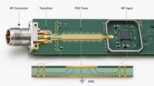
How to Eliminate Ground Loop Problems in Antenna PCB Design?
Antenna PCB design requires extra care because the ground structure is part of the RF system. A poor ground loop can detune the antenna, reduce range or increase radiated noise.
Use these design rules:
- Keep the RF return path short: The antenna feed and ground return should be compact and low impedance.
- Protect the antenna keep-out area: Do not place copper, traces, metal parts or noisy components inside the antenna clearance zone unless required by the antenna design.
- Keep switching circuits away from the antenna: DC-DC converters, clocks, relays and high-current traces can couple noise into the RF path.
- Use proper ground stitching: Place ground vias around RF transmission lines, connectors and board edges to control return current and shielding.
- Control coax shield grounding: For SMA, U.FL, IPEX or other antenna connectors, the shield ground should be close, stable and compatible with the enclosure.
- Avoid long chassis-current paths near RF areas: Chassis or shield current should not flow through the antenna ground region.
- Match the final enclosure condition: Plastic housing, metal housing, battery position and cable routing can all change antenna performance.
- Test after assembly: Measure RF performance after the PCB is installed in the real product, not only on the open bench.
To eliminate ground loop antenna PCB problems, the antenna, ground plane, connector, shield and enclosure should be reviewed as one RF system.

FAQs About PCB Ground Loop
Q1: Can a PCB ground loop happen on a 2-layer PCB?
A1: Yes. A 2-layer PCB can have a ground loop when ground copper is broken, return paths are long, or cables create extra ground routes. The risk is higher when high-current loads and sensitive signals share the same return path. Good copper pour, short loops and ground stitching are important on 2-layer boards.
Q2: Does a 4-layer PCB automatically prevent ground loops?
A2: No. A 4-layer PCB usually provides a better ground plane, but poor placement, split planes, bad connector grounding or chassis current can still create a loop. Layer count helps only when the return path is designed correctly. A solid ground plane does not replace system-level grounding review.
Q3: Can a PCB ground loop appear only after PCBA assembly?
A3: Yes. Bare PCB testing checks continuity and isolation, but it does not test operating current, cable shields, enclosure contact or component behavior. A PCB ground loop often appears only after PCBA assembly and system connection. Functional testing under real load is necessary before mass production.
Q4: Are ground loops only a problem in analog circuits?
A4: No. Analog circuits are sensitive, but digital, RF and power circuits can also suffer from ground loop problems. Digital systems may show reset, jitter or communication errors. RF modules may lose antenna performance, while power circuits may create EMI problems through large return-current loops.
Q5: Can differential signals avoid ground loop noise?
A5: Differential signals improve noise immunity, but they do not remove the need for a proper return path. USB, CAN, RS-485, Ethernet and LVDS can still suffer from common-mode noise. Shield grounding, reference design and cable routing still need to be checked.
Q6: Should cable shields connect to PCB ground or chassis ground?
A6: It depends on the product structure, EMI target and safety requirement. Many designs connect the shield to chassis near the connector and control its connection to signal ground. Directly sending shield current into sensitive PCB ground may create noise, especially in long-cable systems.
Q7: Can a 0-ohm resistor help during grounding debugging?
A7: Yes, a 0-ohm resistor can provide a selectable ground tie point during prototype testing. It helps engineers compare grounding options without redesigning the board immediately. However, it should not carry uncontrolled high current or replace a properly planned return path.
Q8: Are ferrite beads a reliable solution for PCB ground loops?
A8: Ferrite beads may reduce some high-frequency noise, but they are not a complete ground loop fix. A bead between grounds can also create impedance and ground voltage difference. It should be used only after current path, frequency range and load condition are understood.
Q9: When should isolation be used to solve ground loop problems?
A9: Isolation is useful when two systems have different ground references, long cables, high voltage or safety separation requirements. Common options include digital isolators, optocouplers, transformers and isolated DC-DC modules. Isolation adds cost and space, so it should be selected for clear electrical or safety reasons.
Q10: Can PCB test points help find a ground loop?
A10: Yes. Proper test points help measure ground voltage difference, ripple and noise at important locations. Useful locations include power input ground, analog reference ground, switching power ground, connector ground and chassis ground. Without test points, debugging may require risky probing or rework.
Q11: What PCB manufacturing issues can worsen grounding reliability?
A11: Poor via plating, over-etching, weak copper balance, solder mask misregistration and uncontrolled stack-up can affect grounding quality. Manufacturing cannot fix a bad design, but stable fabrication protects the intended ground path. DFM review and inspection are useful before batch production.
Q12: What should buyers provide for grounding review before production?
A12: Buyers should provide schematic files, PCB layout, Gerber files, stack-up requirements, BOM, cable diagram, enclosure drawing and test conditions. Cable and chassis information is especially important because many loops are created outside the PCB. Gerber files alone are not enough for complete review.
Q13: Does copper thickness reduce PCB ground loop risk?
A13: Thicker copper can reduce resistance and support higher current, but it does not remove an uncontrolled loop. Copper thickness helps only when the current path is short and correctly placed. For high-current designs, trace width, via count, copper balance and thermal control should be reviewed together.
Q14: What industries should pay more attention to PCB ground loops?
A14: Medical devices, industrial control, automotive electronics, RF modules, audio systems, test instruments and sensor equipment should pay close attention. These products often combine weak signals, long cables, metal enclosures and strict EMI requirements. Early grounding review can reduce certification and reliability risks.
Q15: How can EBest PCB support PCB projects with grounding risks?
A15: EBest PCB is a China source factory supporting custom PCB fabrication and PCBA assembly for global OEM/ODM projects. We can assist with DFM review, stack-up communication, fabrication inspection, PCBA testing and production risk control. Early review helps reduce noise, EMI and reliability problems before batch production.
Conclusion
A PCB ground loop is a return-current control problem that can affect analog accuracy, EMI performance, RF stability, communication reliability and final product consistency. The best solution is to control the current path early, keep ground impedance low, avoid uncontrolled loops and test the PCB under real system conditions.
EBest Circuit is a China source factory providing custom PCB fabrication, PCBA assembly, DFM review and global supply support for OEM/ODM projects. If your project involves grounding noise, EMI risk, antenna PCB design or mixed-signal PCB production, contact us for technical review and quotation: sales@bestpcbs.com.