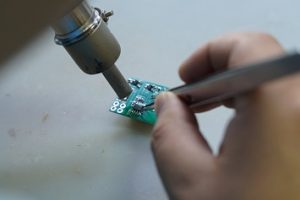
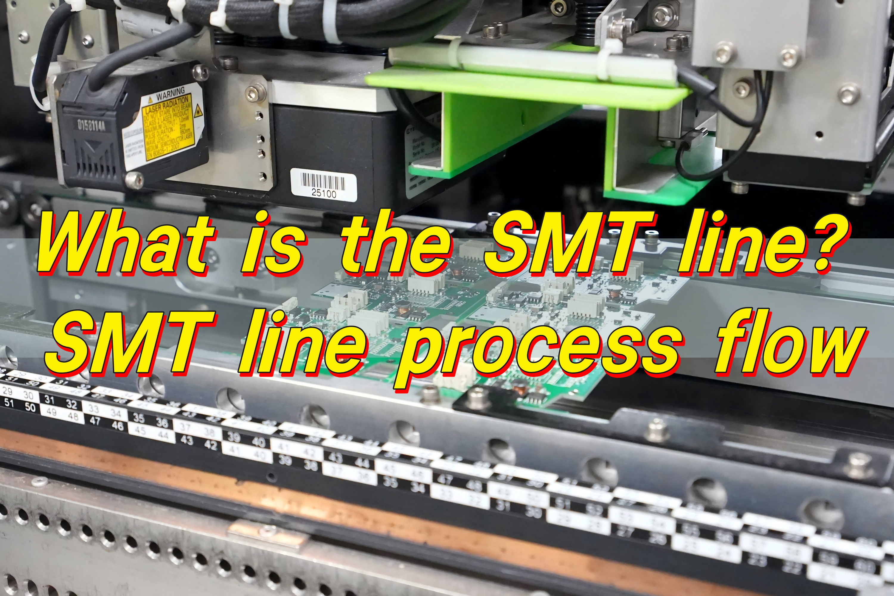
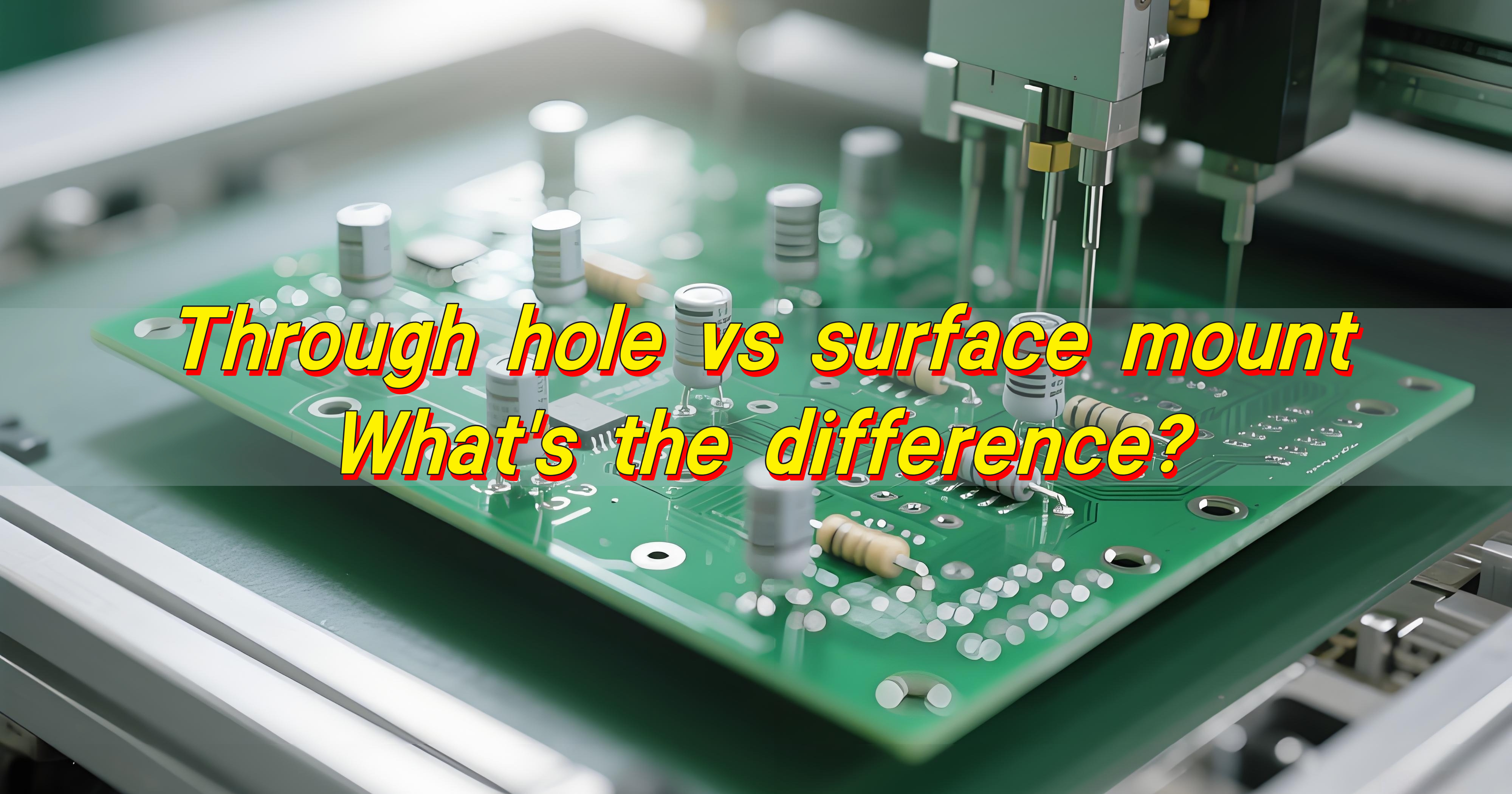
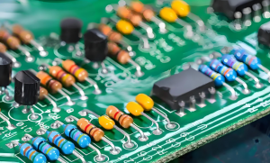
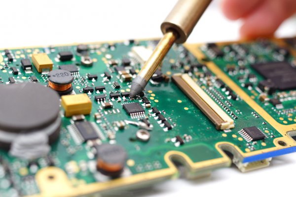
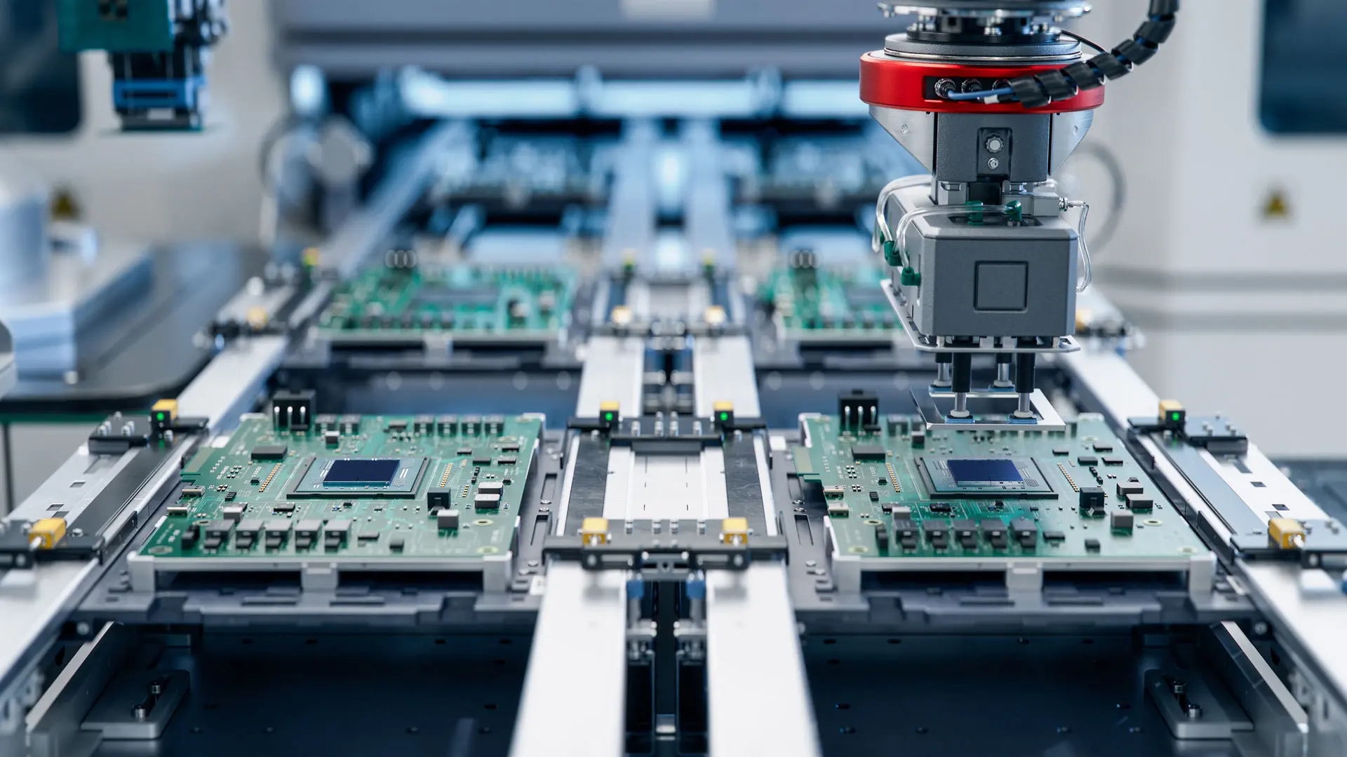
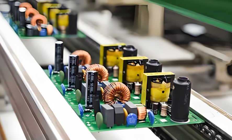
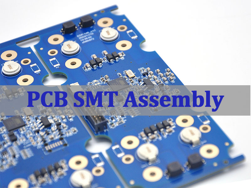
PCB SMT assembly is a highly automated manufacturing method in which surface-mount devices (SMDs) are accurately placed and soldered onto a printed circuit board through controlled reflow processes, enabling high-density circuit layouts, consistent electrical performance, and efficient mass production. This article explains what PCB SMT assembly is, how the process works, what equipment and quality controls are involved, and how engineers can select a reliable SMT assembly partner for prototypes and production.
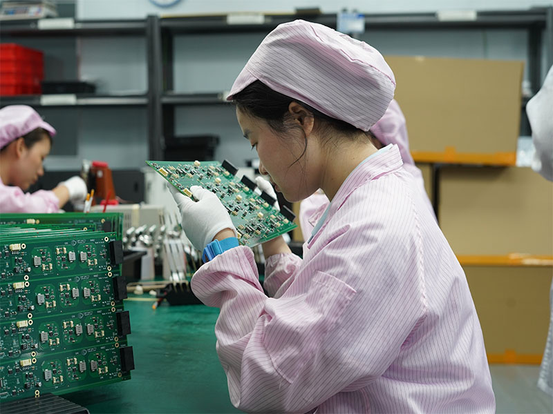
EBest Circuit (Best Technology) places a high priority on engineering quality, process control, and long-term customer collaboration, supported by strong professional talents across PCB fabrication and SMT assembly. Our technical team includes multiple engineers with over 20 years of hands-on PCB and PCBA experience, and several senior engineers and customer managers who have worked at our company for more than 10 years, ensuring continuity and deep product understanding. As a self-owned factory, every project is supported by a dedicated project coordinator, so customers do not need to worry about production progress or delivery schedules—process visibility and lead-time control are built into our workflow. For project inquiries or technical discussions, pls feel free to contact us directly at sales@bestpcbs.com.
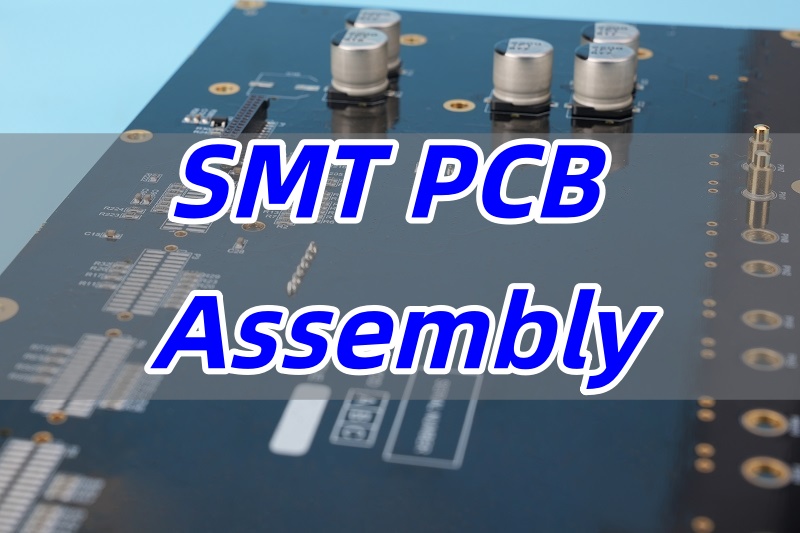
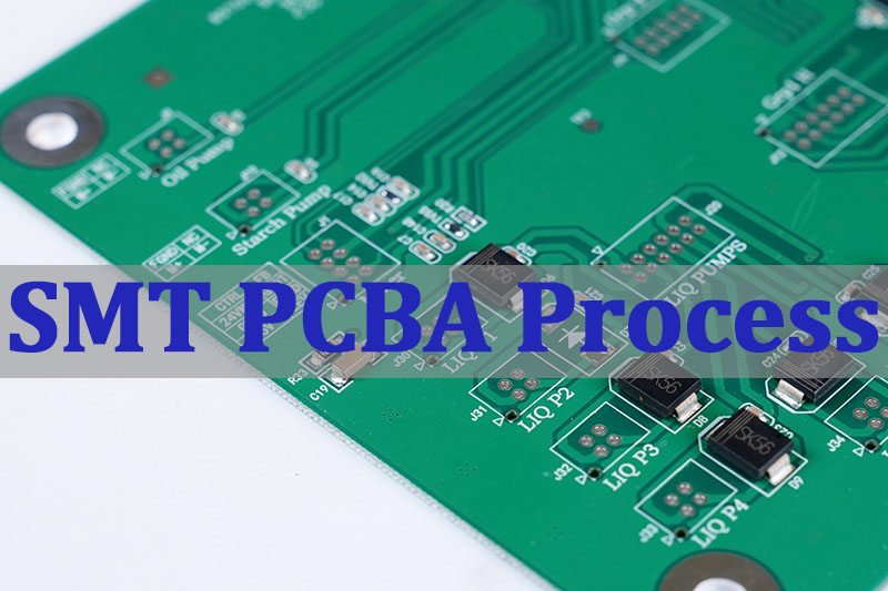
What Is PCB SMT Assembly?
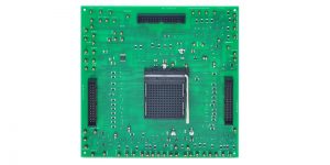
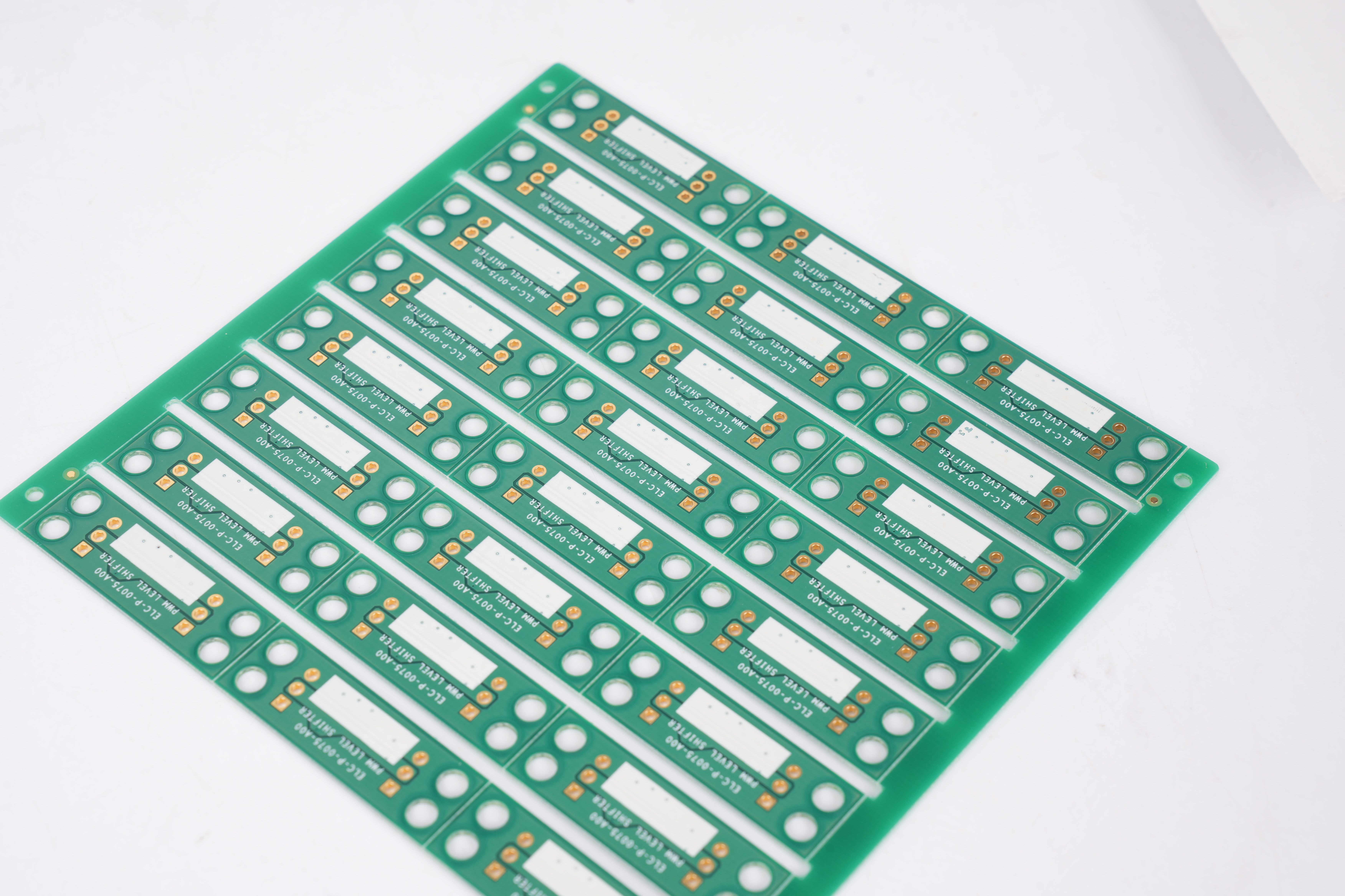
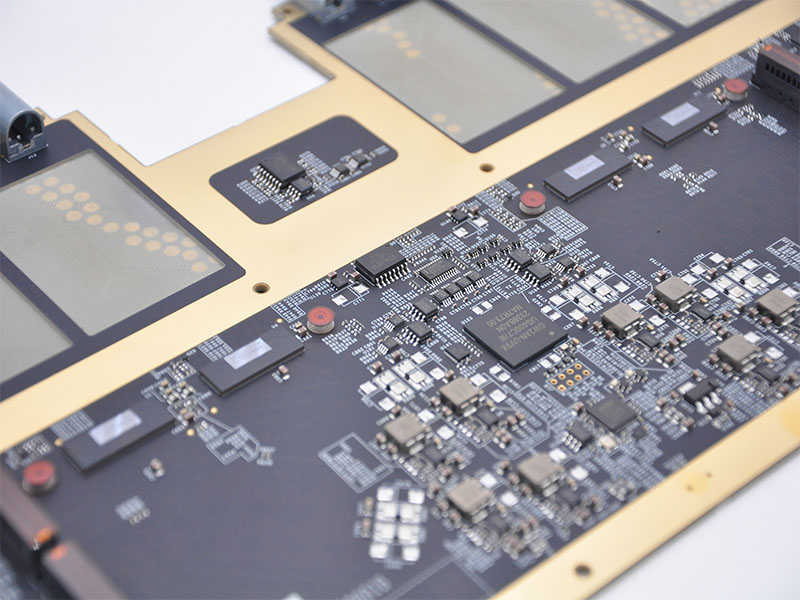
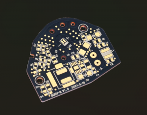
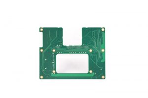
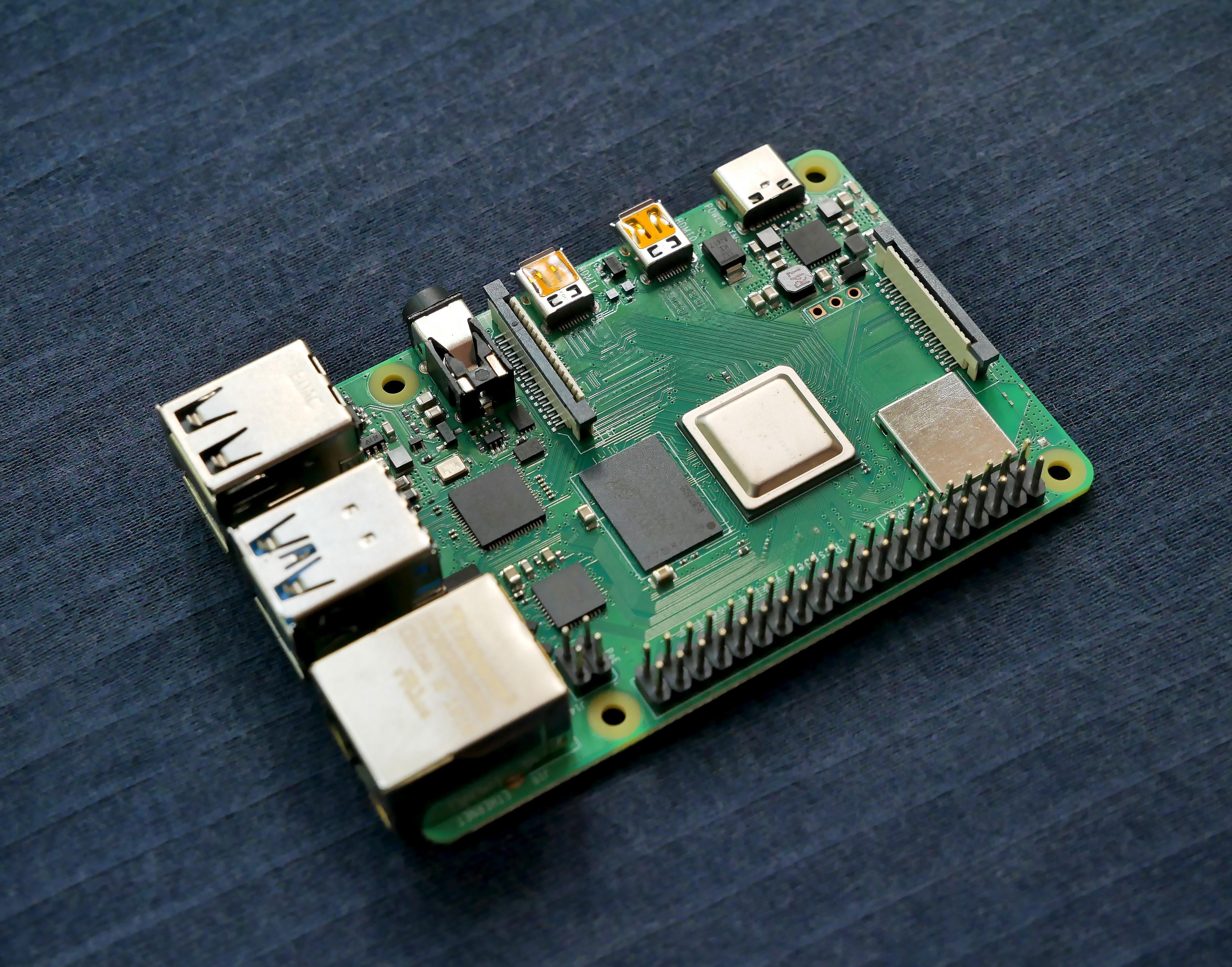
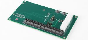
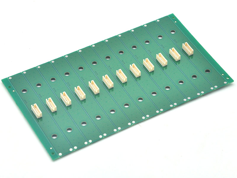
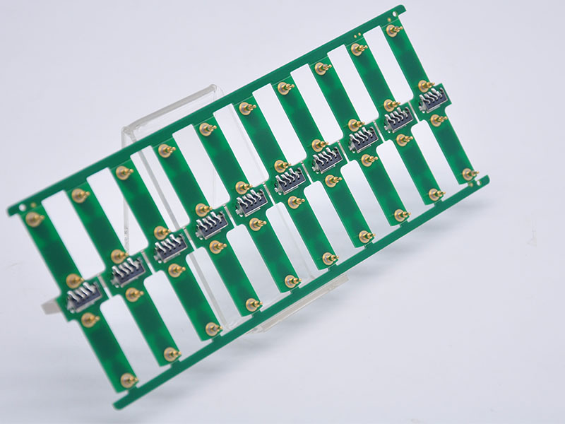
PCB SMT assembly refers to the process of mounting surface-mount devices (SMDs) directly onto the surface of a printed circuit board using automated placement and reflow soldering. It is the backbone of modern electronics manufacturing, enabling compact layouts, higher signal integrity, and scalable production.
From prototype validation to wholesale electronics production, PCB SMT assembly allows engineers to balance performance, manufacturability, and cost. Compared with legacy through-hole methods, SMT supports finer pitch components, double-sided layouts, and high-speed signal routing without sacrificing reliability.
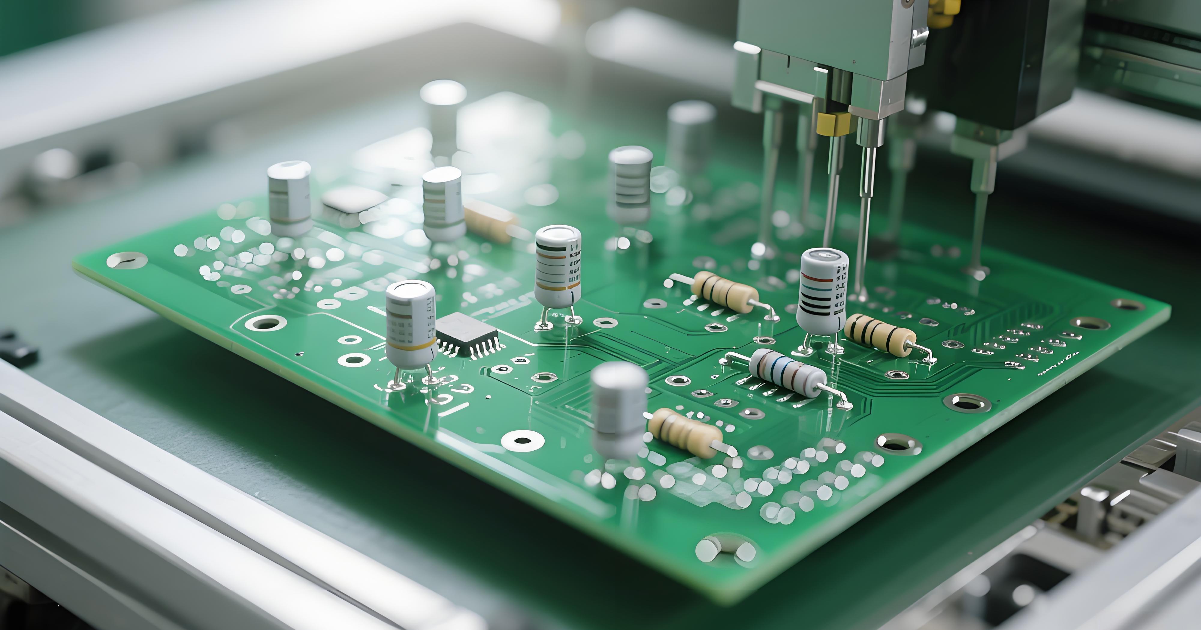
PCB SMT Assembly Process Explained Step by Step
The SMT PCB assembly process is a tightly controlled sequence. Each stage builds on the previous one, and small deviations compound quickly if not engineered upfront.
Step 1: Solder Paste Printing
- Stainless steel SMT stencil for PCB assembly defines paste volume
- Paste height consistency directly affects solder joint strength
- Misalignment at this stage is a leading cause of bridging defects
Step 2: Component Placement
- High-speed SMT placement machines mount chips, QFNs, and BGAs
- Placement accuracy typically ranges from ±25 μm to ±40 μm
- Fine-pitch and BGA parts demand calibrated feeders and vision alignment
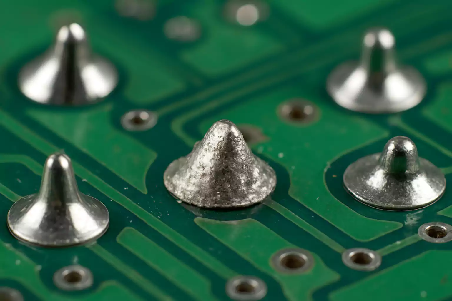
Step 3: Reflow Soldering
- Multi-zone reflow profiles activate solder paste gradually
- Lead-free SMT PCB assembly requires higher peak temperatures
- Thermal symmetry prevents warpage and head-in-pillow defects
Step 4: Inspection and Testing
- AOI checks polarity, offset, and solder fillet shape
- X-ray inspection is mandatory for BGA PCB SMT assembly
- Electrical testing validates functional integrity
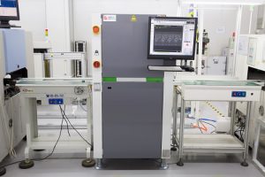
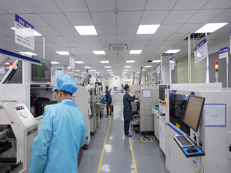
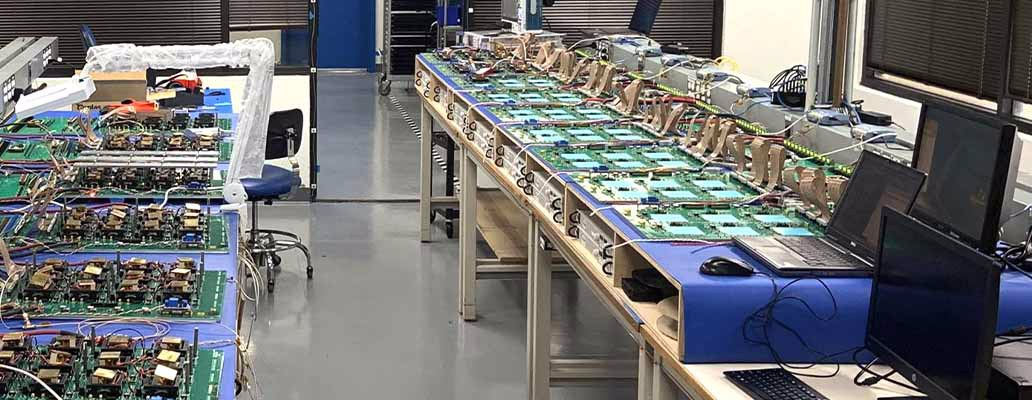
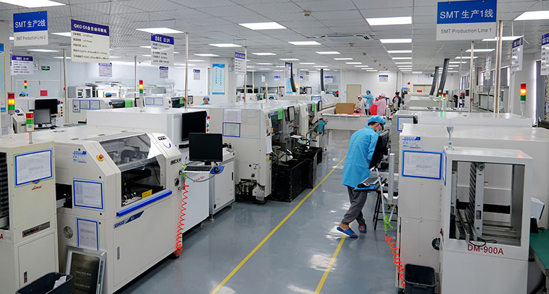
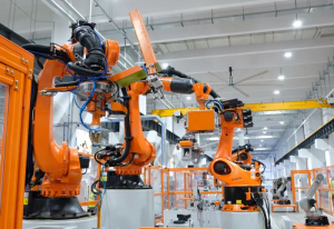
Key SMT PCB Assembly Equipment and Machines
Process capability in SMT PCB assembly depends more on equipment integration than on labor count.
Core equipment used in professional SMT lines
| Equipment | Function | Engineering Impact |
|---|---|---|
| Solder paste printer | Applies uniform paste | Determines solder joint volume |
| SMT placement machine | Places components | Affects accuracy and yield |
| Reflow oven | Solder activation | Controls metallurgical quality |
| AOI system | Optical inspection | Detects visible defects |
| X-ray inspection | Internal joint check | Essential for BGA reliability |
A stable SMT PCB assembly line is defined by repeatability, not speed alone.
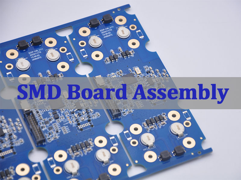
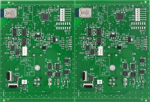
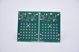
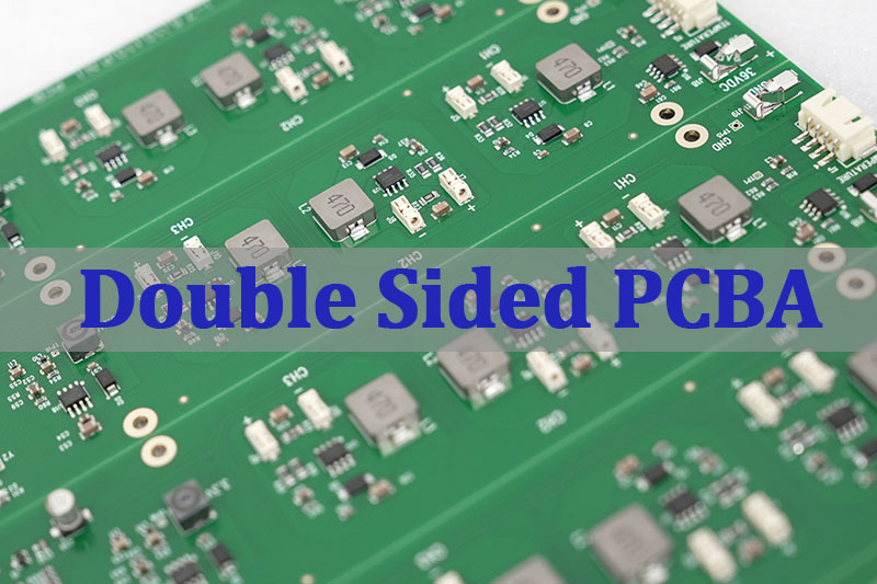
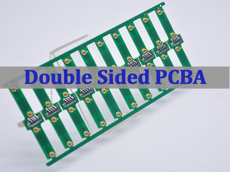
Double-Sided and High-Density PCB SMT Assembly Capabilities
Why double-sided SMT increases engineering difficulty
- Secondary reflow risks component shift or drop
- Copper balance affects thermal behavior
- Process windows narrow significantly
Typical applications
- PCB SMT assembly double sided industrial control boards
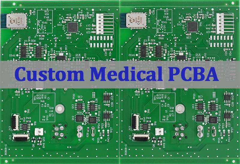
- Compact consumer and medical electronics
- HDI PCB custom service SMT assembly circuit boards
Without DFM review, double-sided designs often suffer yield loss during scaling.
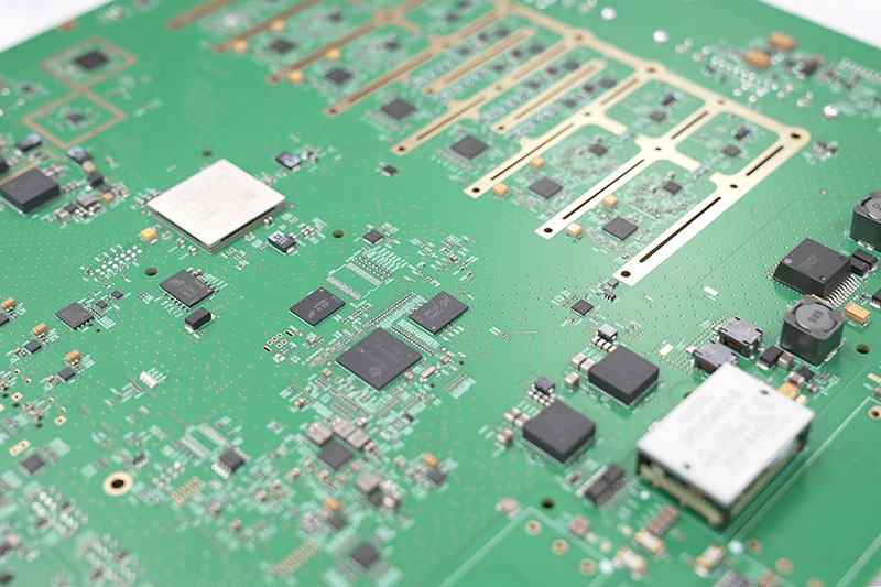
BGA, Fine-Pitch, and HDI PCB SMT Assembly Challenges
BGA PCB SMT assembly introduces hidden solder joints and higher inspection complexity.
Common risks in advanced SMT
- Head-in-pillow due to oxidation or profile mismatch
- Voids caused by trapped flux gases
- PCB warpage in high-layer HDI boards
Engineering countermeasures
- Nitrogen-assisted reflow
- X-ray sampling with defined acceptance criteria
- Stencil aperture reduction for BGA pads
Prototype vs Wholesale PCB SMT Assembly: Cost and Risk Differences
| Item | Prototype SMT PCB Assembly | Wholesale SMT PCB Assembly |
|---|---|---|
| Primary goal | Speed and validation | Cost and consistency |
| BOM flexibility | High | Low |
| Process tuning | Manual + adaptive | Locked and repeatable |
| Risk tolerance | Higher | Very low |
Trying to apply wholesale pricing logic to prototype projects often leads to rework and schedule overruns.
Common SMT PCB Assembly Defects and How to Prevent Them
Typical SMT assembly defects
| Defect Type | Root Cause | Prevention Method |
|---|---|---|
| Solder bridging | Excess paste | Stencil aperture tuning |
| Tombstoning | Thermal imbalance | Pad symmetry control |
| Insufficient solder | Low paste volume | Printer calibration |
| BGA voids | Flux entrapment | Profile optimization |
Defect prevention always starts at PCB design and SMT assembly guidelines, not at inspection.
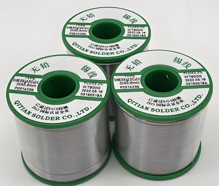
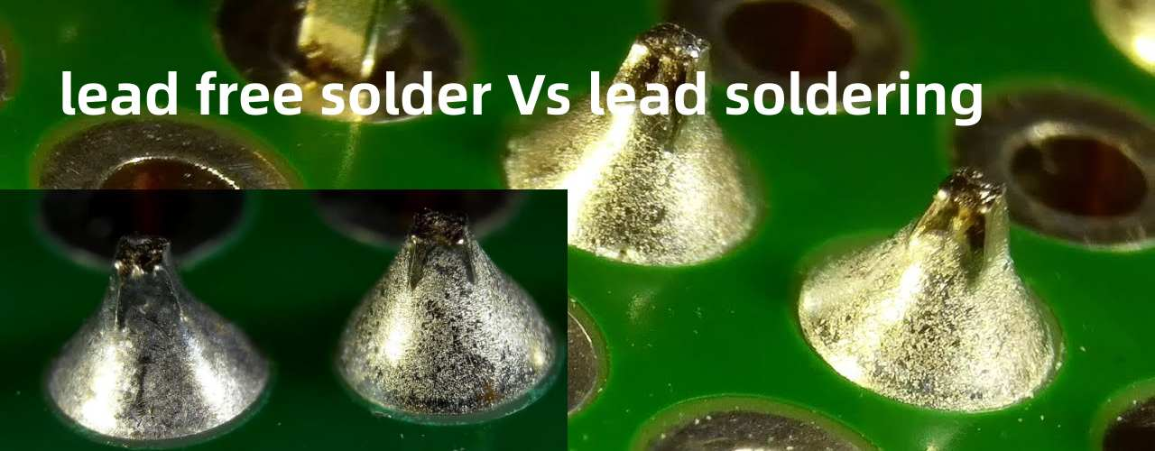
Lead-Free and High-Reliability PCB SMT Assembly Standards
Lead-free PCB SMT assembly places significantly higher demands on thermal control and process stability compared with traditional tin-lead soldering, as elevated reflow temperatures reduce the allowable process window and increase stress on both components and PCB materials.
Key engineering implications of lead-free SMT
- Higher peak reflow temperatures
Lead-free alloys typically require peak temperatures in the 235–250 °C range, increasing the risk of PCB warpage, component cracking, and solder joint fatigue if profiles are not precisely controlled. - Greater sensitivity to PCB material selection
PCB laminate Tg, Td, and CTE become critical under lead-free conditions. Inadequate material choices can lead to delamination, pad lifting, or micro-cracking during reflow. - Stronger need for documented process control
Lead-free SMT demands tightly defined reflow profiles, verified thermal uniformity, and repeatable machine settings, all supported by controlled work instructions and change management.
For high-reliability PCB SMT assembly, compliance extends beyond soldering itself. These applications require full material and process traceability, validated reflow profiles, and documented inspection criteria such as AOI and X-ray acceptance standards to ensure consistent quality across production batches.
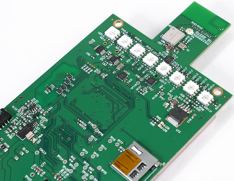
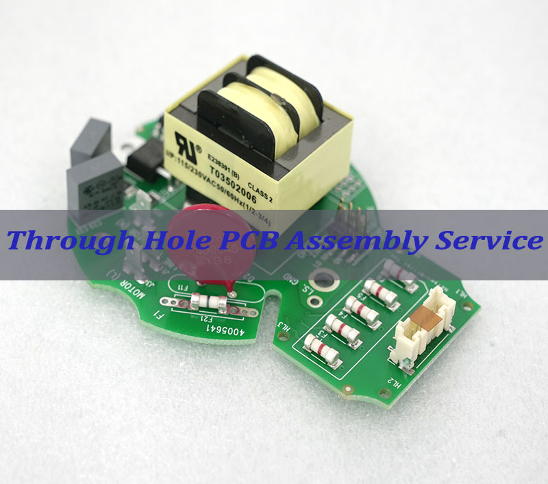
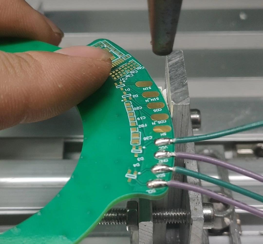
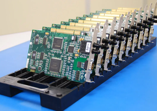
Flex, Rigid-Flex, and Mixed SMT/THT PCB Assembly
Flex PCB SMT assembly
- Requires dedicated support fixtures
- Lower placement force to avoid deformation
- Stress-aware reflow profiles
Mixed board assembly SMT THT PCB
- SMT completed first
- THT handled via selective soldering
- Protects sensitive SMT joints
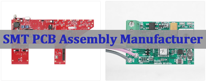
How to Choose a Reliable PCB SMT Assembly Manufacturer?
Engineers should evaluate capability beyond surface claims.
Practical selection criteria
- In-house SMT PCB assembly equipment
- DFM review before quotation
- Proven BGA and HDI experience
- Digital traceability across materials and processes
A reliable PCB SMT assembly manufacturer explains risks clearly instead of hiding them in pricing.
PCB SMT Assembly Cost Structure and Quotation Logic
What actually drives SMT assembly cost
- Component sourcing volatility
- Assembly complexity (BGA, double-sided, HDI)
- Inspection depth (AOI vs X-ray coverage)
- Yield risk
Transparent quotations clarify trade-offs and avoid surprises during production.
To sum up, PCB SMT assembly is a process-driven manufacturing discipline that directly determines product reliability, yield stability, and time-to-market.
Our strength lies in engineering-led SMT execution (technical team support and DFM pre-review), one-stop PCB manufacturing, component sourcing, and PCBA integration, and fast-turn PCBA delivery with digital traceability. If you need dependable PCB SMT assembly for prototypes or production, pls feel free to contact us via sales@bestpcbs.com.
FAQ: PCB SMT Assembly
Q1: What is SMT in PCB assembly?
SMT in PCB assembly refers to Surface Mount Technology, where electronic components are mounted directly onto the surface of a printed circuit board using automated placement and reflow soldering. This method supports higher component density, smaller board size, and efficient mass production.
Q2: Is SMT PCB assembly suitable for low-volume projects?
Yes. Prototype SMT PCB assembly supports fast design verification.
Q3: How reliable is BGA SMT assembly?
With X-ray inspection and controlled profiles, BGA reliability is very high.
Q4: What files are required for SMT PCB assembly?
Gerbers, BOM, centroid file, assembly drawing, and test requirements.
Q5: Can SMT and THT be combined on one board?
Yes. Mixed SMT/THT PCB assembly is common in industrial designs.
Q6: How long does PCB SMT assembly take?
Typical lead time is 7–10 working days, depending on sourcing.
Q7: How much does PCB SMT assembly cost?
PCB SMT assembly cost depends on factors such as component count, board complexity, package types (BGA, fine-pitch), inspection requirements, and production volume. Prototype assemblies typically cost more per unit than volume production due to setup and sourcing overhead.
Q8: What equipment is used in SMT assembly?
SMT assembly uses solder paste printers, pick-and-place machines, reflow ovens, AOI systems, and X-ray inspection equipment. These machines work together to ensure placement accuracy, solder joint quality, and process consistency.
Q9: What is the difference between PCB fabrication and SMT assembly?
PCB fabrication focuses on manufacturing the bare circuit board, while SMT assembly involves mounting and soldering electronic components onto the finished PCB. Both processes are essential but occur at different stages of electronics production.
Q10: What are the limitations of SMT in PCB assembly?
SMT is less suitable for very large or high-power components that require strong mechanical support. It also demands tighter process control and higher upfront equipment investment compared to traditional through-hole assembly.