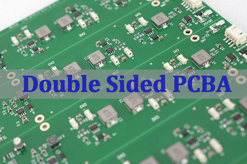
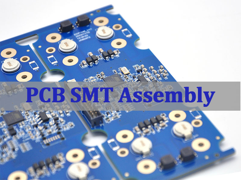
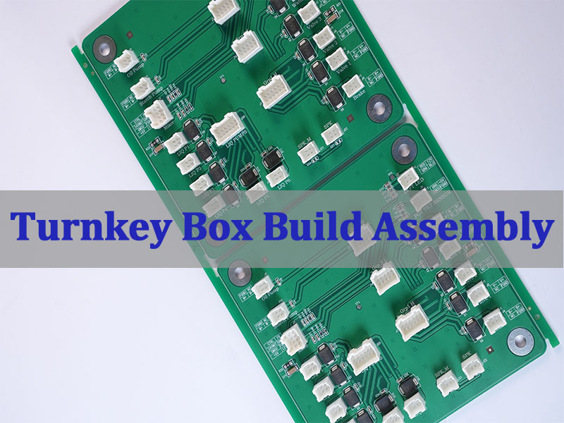
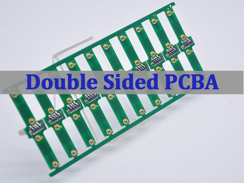
Double sided PCBA is becoming a mainstream solution for compact electronic devices that require higher density without increasing board size. This article explains design logic, manufacturing flow, reliability control, and supplier evaluation from an engineer’s perspective to help readers understand how double sided PCBA projects achieve stable yield and fast delivery.
As one of the top electronic PCB PCBA manufacturers in China, EBest Circuit (Best Technology) provides a professional 2L PCB PCBA solution for global electronics manufacturing. Our team is formed by experienced professional talents who understand real production challenges, while a dedicated project coordinator follows each project from DFM review to final shipment, ensuring every pre-requisire is confirmed before manufacturing starts. Reliability is always our first priority, and our engineers take a proactive role in risk analysis, material planning, and process optimization to minimize uncertainty for customers.
Through disciplined quality control and continuous improvement, we strive to outdo conventional PCBA service standards and build lasting trust with engineers who value consistency, traceability, and dependable delivery. If you are sourcing double sided PCBA, our engineering team provides fast-response manufacturing support. A warm welcome to contact us at sales@bestpcbs.com for project discussion.
What Is Double Sided PCBA and How Is It Different from Standard PCB Assembly?
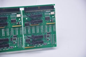
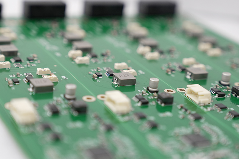
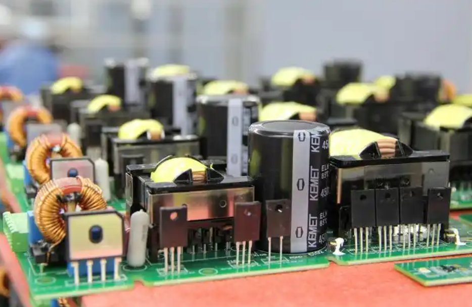
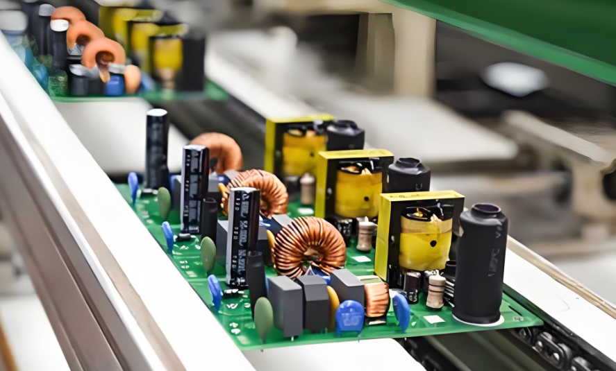
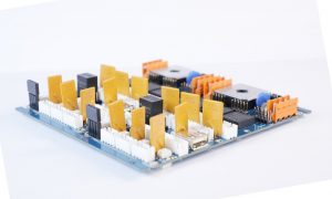
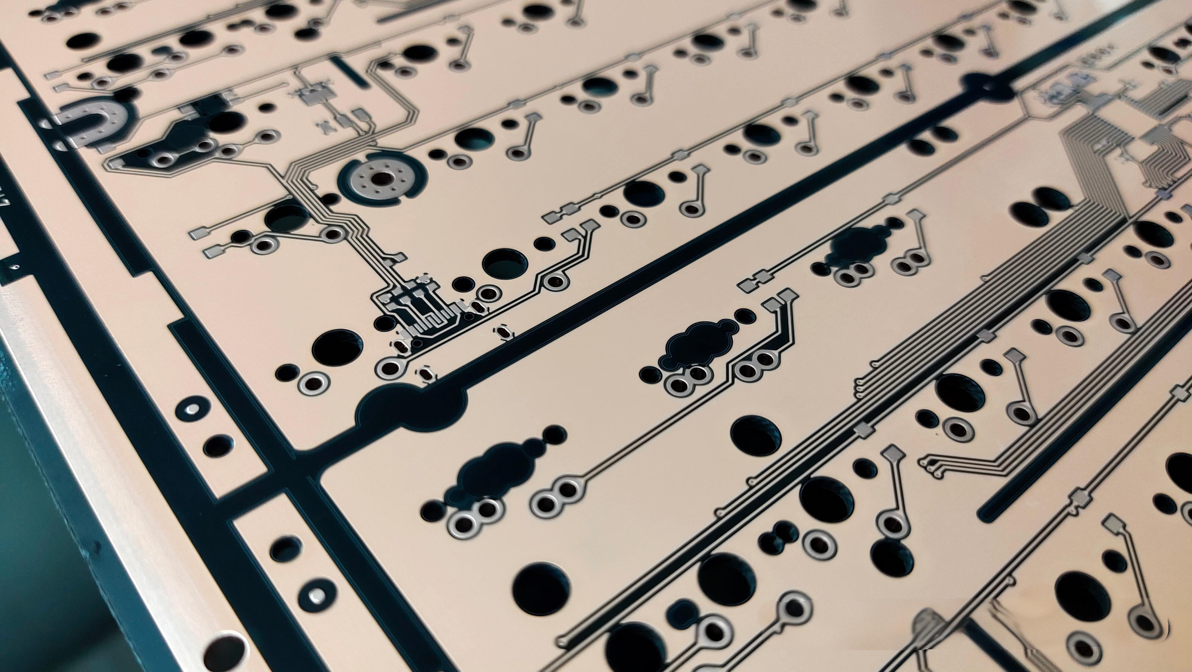
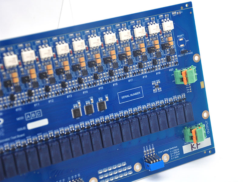
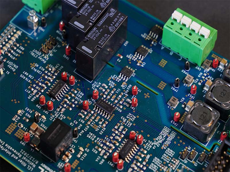
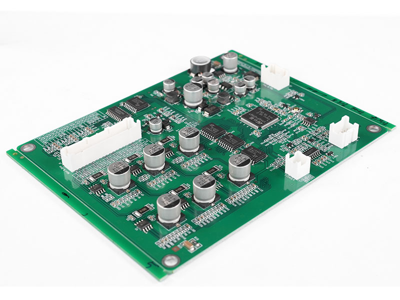
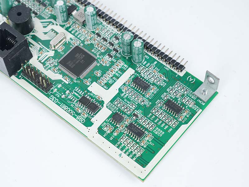
Double sided PCBA means components are mounted on both sides of a printed circuit board, increasing functional density without expanding PCB area. Compared with single-sided assembly, it introduces extra thermal control and process sequencing challenges.
How does double-sided assembly work?
- Top-side SMT reflow is completed first
- Adhesive or pallet support protects bottom components
- Second-side reflow uses optimized temperature curves
Why engineers prefer double-sided layouts
- Higher circuit integration
- Reduced enclosure size
- Better routing flexibility
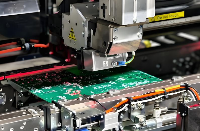
In double sided PCB PCBA projects, placement order directly affects solder joint reliability.
Why Are Electronics Moving Toward Double Sided PCB PCBA Designs?
Modern electronics require compact layouts with stable electrical performance. Double sided assembly allows engineers to integrate analog, power, and high-speed signals within limited space.
Common industries adopting double sided PCBA
- Industrial automation controllers
- Medical monitoring equipment
- Communication modules
- Automotive electronics
The demand for electronics double-sided multilayer PCBA printed circuit boards keeps increasing as product miniaturization accelerates.
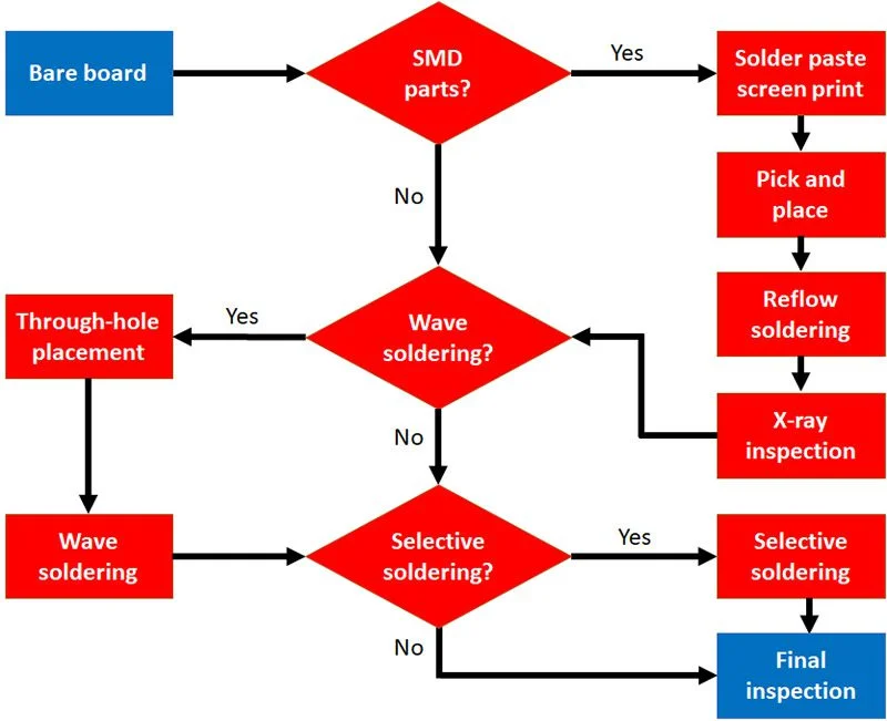
What Is the Manufacturing Flow of China Double Sided PCBA?
A typical China double sided PCBA process follows a controlled sequence to maintain component stability during reflow cycles.
Core process stages
- Solder paste printing
- Top-side SMT placement
- First reflow profiling
- AOI inspection
- Bottom-side placement
- Second reflow or selective soldering
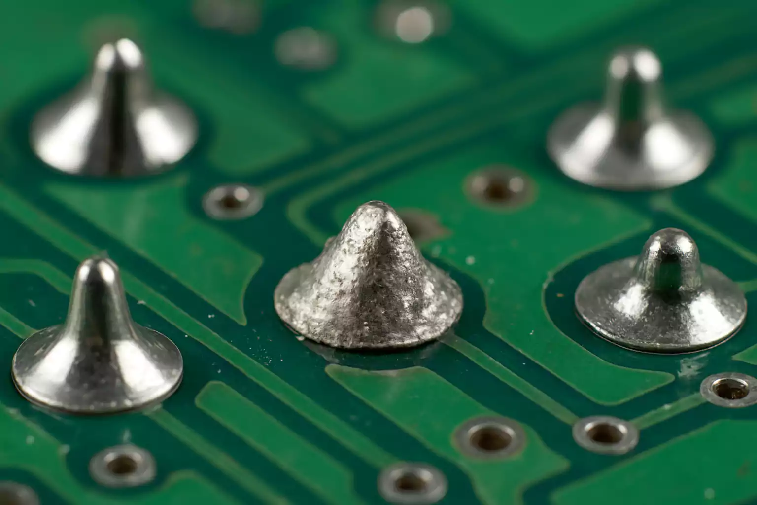
Incorrect thermal balance can lead to tombstoning or misalignment. Experienced factories design process windows based on component weight and solder volume.
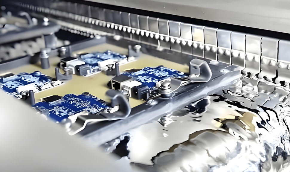
How Do Engineers Prevent Component Drop and Thermal Issues in Double-Sided Assembly?
Component fall-off during the second reflow is a common concern. Engineering teams mitigate risk through material selection and mechanical support.
Key engineering methods
- Red glue or adhesive bonding
- Fixture pallets
- Optimized thermal ramp rates
Thermal management strategies
- Balanced copper distribution
- Controlled peak temperature
- Nitrogen reflow environment
These measures help ensure stable yield for printed circuit board PCBA double-sided pcb board oem multilayer projects.
What Certifications Are Required for High Quality Double Sided PCBA?
High-reliability products require structured quality systems rather than only manufacturing experience.
Typical certifications engineers look for
- ISO 9001 for quality management
- ISO 13485 for medical devices
- IATF 16949 for automotive electronics
- AS9100D for aerospace applications
A qualified supplier offering superior quality double sided PCBA should demonstrate traceability from PCB fabrication to final testing.
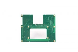
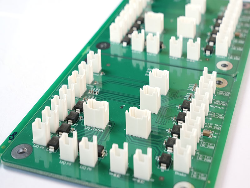
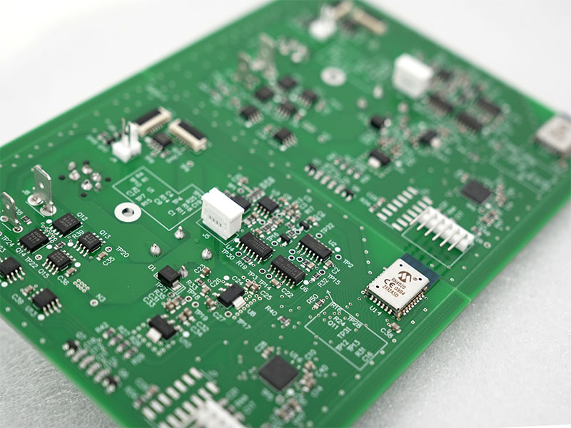
Key Design Guidelines for Electronics Double-Sided Multilayer PCBA Printed Circuit Boards
Design rules strongly influence assembly yield. Engineers must consider mechanical and electrical constraints simultaneously.
Layout recommendations
- Avoid placing heavy connectors on both sides in the same area
- Use via stitching to improve thermal balance
- Maintain consistent component height
Stack-up considerations
- Balanced copper layers
- Controlled impedance routing
- Stable solder mask alignment
Proper design reduces manufacturing complexity and improves long-term reliability.
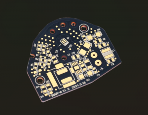
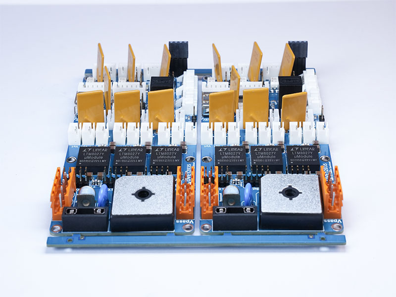
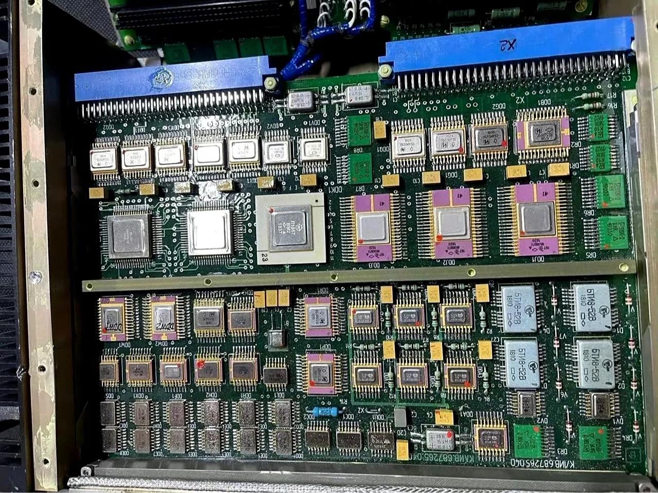
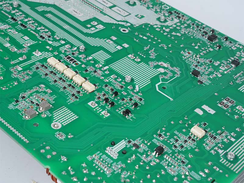
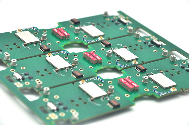
Advantages of Printed Circuit Board PCBA Double-Sided PCB Board OEM Multilayer
Double sided assembly offers structural benefits that extend beyond simple density improvements.
Engineering advantages
- Shorter signal paths
- Reduced EMI
- Lower system cost compared to adding extra layers
Production benefits
- Faster assembly cycles
- Reduced enclosure volume
- Flexible component arrangement
OEM multilayer solutions frequently combine HDI routing with double sided placement for advanced electronics.
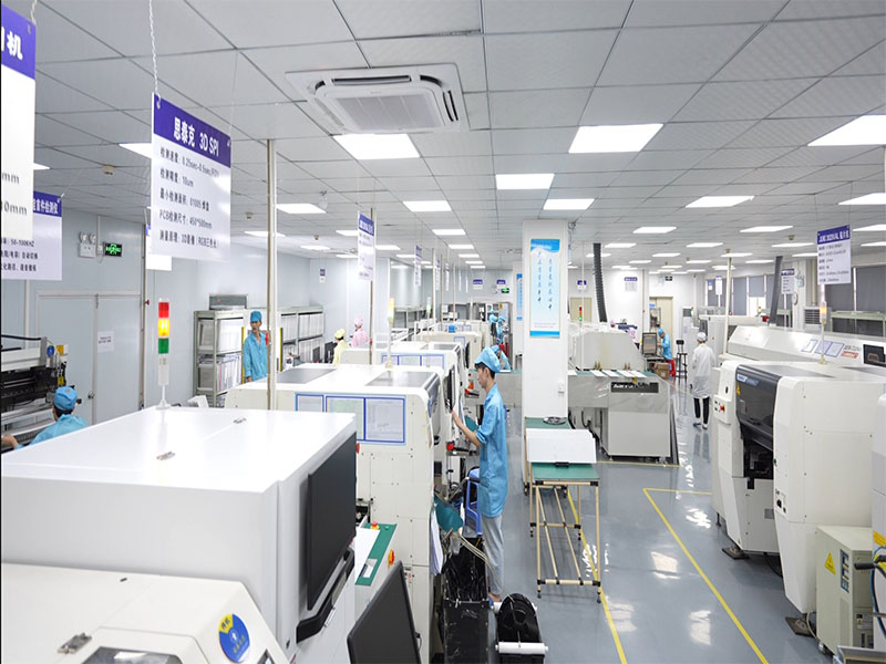
How to Evaluate a China Double Sided PCBA Manufacturer Capability?
Selecting a supplier requires more than reviewing equipment lists. Engineers focus on process stability and inspection coverage.
Capability checklist
- Dual reflow line configuration
- SPI + AOI + X-ray inspection
- Fine-pitch placement accuracy
- Thermal profile database
A reliable China double sided PCBA partner usually provides DFM feedback before production begins.
Cost Structure and Lead-Time Planning for Double Sided PCBA Projects
Project cost is affected by component count, inspection requirements, and reflow complexity.
Main cost drivers
- SMT setup and stencil preparation
- Double reflow cycle time
- Inspection coverage level
Lead-time optimization tips
- Use standard component packages
- Provide complete BOM early
- Confirm stack-up during DFM stage
Engineers often reduce risk by running small pilot batches before mass production.
Common Failure Modes and Engineering Optimization for Double Sided PCBA
Even mature processes can encounter assembly challenges.
Typical failure issues
- Tombstoning of small passives
- Shadowing during reflow
- Warpage on thin boards
Optimization approaches
- Adjust solder paste volume
- Modify component orientation
- Improve PCB rigidity
Continuous process refinement ensures stable output for electronics double-sided multilayer PCBA printed circuit boards.
China Double Sided PCBA vs Local Assembly: How Should Engineers Decide?
Choosing between overseas and local production depends on project scale and technical requirements.
When China double sided PCBA makes sense
- Medium to high volume production
- Complex multilayer structures
- Cost-sensitive programs
When local assembly is preferred
- Ultra-fast prototypes
- Low-volume engineering samples
Hybrid supply models are increasingly common for global engineering teams.
In a nutshell, double sided PCBA enables compact electronic design by maximizing board utilization while maintaining high reliability through controlled engineering processes. Our team provides strong engineering-driven manufacturing support, including advanced DFM review with BOM optimization, a dedicated multidisciplinary engineering team for full-process coordination, and fully integrated PCB and PCBA factories with digital traceability systems, helping engineers accelerate product launch with confidence.
FAQ About Double Sided PCBA
What is the biggest challenge in double sided PCBA assembly?
Thermal balancing between two reflow cycles is the most critical factor affecting yield.
Can heavy components be placed on both sides?
Yes, but fixture support or adhesive bonding is usually required.
Is double sided PCBA more expensive than single sided?
Initial setup cost is higher, but system-level cost can decrease due to higher integration.
Does multilayer design always require double sided assembly?
Not always. Some multilayer boards still use single-side placement depending on application.