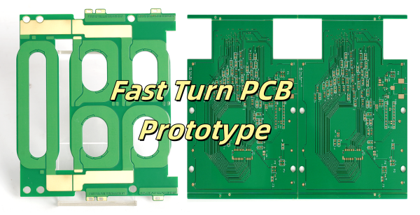
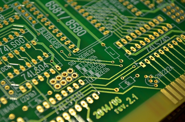
What is Wireless PCB?
Wireless PCB is a printed circuit board specially designed to support wireless communication functions. It integrates various wireless communication modules, antennas and related electronic components, enabling electronic devices to perform data transmission, signal reception and transmission without physical cable connection. For example, the smart phones, tablets, wireless Bluetooth headsets and other devices we use in daily life all use wireless PCB technology, thus realizing convenient Wi-Fi connection, Bluetooth data transmission, NFC near-field communication and other functions.
Compared with traditional PCB, the biggest feature of wireless PCB is its wireless communication capability. Through careful layout and design, it organically integrates circuit modules with different functions such as radio frequency (RF) circuit, baseband processing circuit, power management circuit on a circuit board, and also takes into account the transmission characteristics of wireless signals, such as impedance matching, signal interference and other issues, to ensure the stability and efficiency of wireless communication.
Advantages of wireless PCB
- High flexibility
Because of the wireless PCB, devices can be moved and placed more freely, no longer restricted by the length and connection position of cables. For example, wireless smart home devices can be easily deployed in every corner of the home, and users can control them through mobile phones or other smart terminals anytime and anywhere, it greatly improves the user’s experience.
- Easy to install
In some large-scale applications, such as industrial automation production lines, smart warehousing systems, etc., wireless PCBs can significantly reduce the use of cables. So that reducing material costs, installation costs, and later maintenance costs. Since there is no need to use a large number of cables, the installation process of the equipment is also simpler and faster, which can greatly shorten the lead time.
- Support multi-device interconnection
Wireless PCBs can achieve seamless connection and data sharing between multiple devices. In the Internet of Things (IoT) environment, various smart devices can communicate with each other through the network built by wireless PCBs to form a large and intelligent ecosystem.
- Easy to upgrade and expand
With the continuous development of wireless communication technology, new wireless standards and protocols continue to emerge. The design of wireless PCBs is relatively flexible, which is easy to upgrade and expand to adapt to new technical requirements. For example, when Wi-Fi technology is upgraded from 802.11n to 802.11ac or 802.11ax, only the relevant modules on the wireless PCB need to be updated or optimized without a large-scale redesign of the entire device.
Disadvantages of wireless PCB
- Signal interference problem
Since the wireless PCB works in an open wireless environment, it is easily interfered by others, like wireless devices or electromagnetic signals around it. For example, in areas with crowded Wi-Fi frequency bands, such as offices and apartment buildings, wireless devices may experience signal interruption, slow network speed and other problems.
- High power consumption
In order to realize wireless communication functions, wireless PCB needs to consume a certain amount of power to drive the wireless module and antenna to work. Especially in some devices that adopt high-performance wireless communication standards (such as 5G), the power consumption problem is more prominent. This will not only shorten the battery life of the device, but also may put higher requirements on the heat dissipation design of the device.
- Limited transmission distance
Compared with wired communication, the wireless signal transmission distance of wireless PCB is usually shorter. Although the transmission distance can be extended by increasing antenna power and using repeaters, this will also increase costs and system complexity. In some application scenarios with high transmission distance requirements, such as remote industrial monitoring and large-scale wireless sensor networks, wireless PCBs may need to be combined with other wired or wireless communication technologies to meet the requirements.
Design Guidelines for Wireless PCBs
Designing a wireless PCB requires a balance between functionality, efficiency, and reliability. Engineers must consider several factors to optimize performance while addressing potential challenges.
1. Clarify Design Goals and Requirements
First, determine the specific functions that the wireless PCB needs to implement, such as Wi-Fi connection, Bluetooth communication, ZigBee networking, etc. For example, when designing a wireless PCB for a smart watch, it may be necessary to have Bluetooth communication for connecting to a mobile phone and receiving notifications, as well as low-power Wi-Fi functions for occasional software updates. Clarify the range and data transmission rate requirements of wireless communication. For short-range, low-rate applications, such as the PCB design of a wireless mouse, Bluetooth low-power technology may be sufficient; while for wireless surveillance cameras that require high-speed data transmission, Wi-Fi 6 or higher standard wireless PCB designs can meet the needs.
2. Component selection
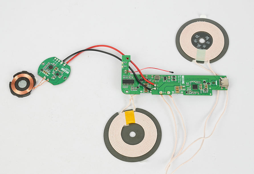
- Wireless module selection
Select the appropriate module according to the designed wireless communication standard. There are various brands and models of Wi-Fi modules, Bluetooth modules, ZigBee modules, etc. on the market. For example, for high-performance Wi-Fi applications, select modules that support Wi-Fi 6 or Wi-Fi 6E standards, which generally have higher data transmission rates and lower power consumption. Investigate the module’s integration and peripheral circuit requirements. Highly integrated modules can simplify PCB design and reduce the number of components.
- Antenna selection
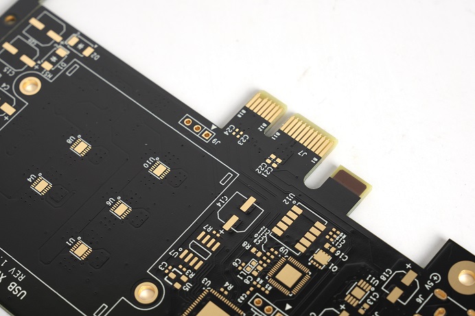
Determine the antenna type. Common antenna types include patch antennas, whip antennas, helical antennas, etc. Patch antennas are suitable for miniaturization and integrated designs inside the PCB; whip antennas are suitable for occasions that require higher gain and longer transmission distances. For example, in wireless vehicle communication devices, whip antennas may be used. Consider the performance parameters of the antenna. Antenna parameters such as gain, bandwidth, and directivity directly affect the effect of wireless communication. When selecting an antenna, it should be determined based on the designed communication distance, frequency range, and signal coverage requirements.
- Other component selection
For power management components, select appropriate regulators, power chips, etc. Ensure that a stable power supply can be provided to the wireless module and other components, and consider the efficiency and power consumption of the power supply. For example, in low-power wireless devices, select a power management chip with low quiescent current. Select appropriate filtering components, such as capacitors and inductors, to filter out power supply noise and signal interference.
3. PCB layout
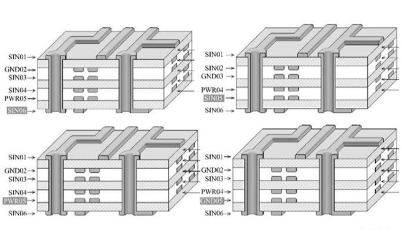
- Partition circuits with different functions
Divide the wireless module, antenna, power circuit, digital circuit, etc. into different areas. For example, place the wireless module and antenna close to the edge of the PCB to reduce signal transmission loss; place the power circuit away from sensitive wireless signal areas to prevent power supply noise from interfering with wireless signals.
- Set up isolation zones
Set up isolation zones between different functional areas, such as through blank copper foil or grounded vias. For example, set up isolation zones between digital circuits and analog circuits to reduce crosstalk between digital signals and analog signals, especially in the analog front-end part that processes wireless signals, where this isolation is more important.
- Component placement
Place components according to the signal flow direction. For wireless communication circuits, start from the antenna input and place RF front-end components, wireless modules, etc. in sequence so that signals can be transmitted smoothly between components. Meanwhile, separate components that generate large amounts of heat from temperature-sensitive components to prevent heat transfer from affecting component performance. At the same time, keep components that may generate electromagnetic interference, such as high-frequency clock components, away from wireless modules and antennas. For example, when laying out, place the high-frequency clock crystal oscillator of the microprocessor away from the wireless module to prevent the high-frequency signal it generates from interfering with wireless communication.
4. PCB traces design
For wireless signal transmission lines, their characteristic impedance must be strictly controlled. Usually, the characteristic impedance of the transmission line of a wireless circuit is designed to be 50Ω or 75Ω. Use appropriate line width and dielectric thickness to achieve impedance matching, and try to maintain the uniformity of the transmission line to avoid impedance mutations.
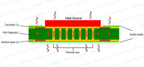
5. Electromagnetic compatibility (EMC) design
A metal shielding cover can be used or a shielding layer can be formed by copper plating on the PCB. For example, for sensitive Wi-Fi modules, metal shielding covers are used to surround them. The shielding covers should be well grounded, which can effectively prevent external electromagnetic interference from entering the module and reduce the electromagnetic radiation of the module itself.
6. Signal integrity analysis
Use professional signal integrity analysis software, such as HyperLynx, to analyze the reflection and crosstalk of the signal on the wireless PCB. By simulating the transmission process of the signal on the transmission line, find out where the reflection may occur, such as the end point and branch point of the transmission line.
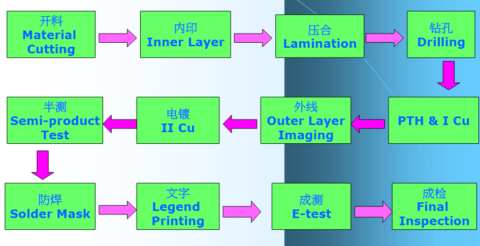
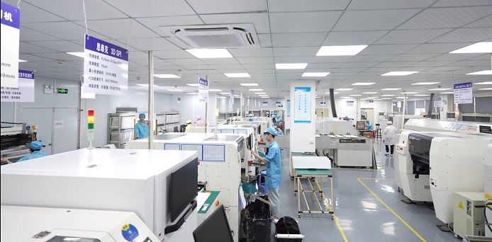
Wireless PCB Assembly Process
Wireless PCB assembly involves mounting and soldering components onto the board to create a functional circuit. The process demands precision due to the small size and sensitivity of components used in wireless communication. Key steps include:
1. Check the PCB board: Ensure that the PCB board is free from scratches, deformation, short circuit and other defects, and the surface of the welding pad of each component is clean and free of oxidation.
2. Check the component list: Check the part number, specification and quantity of the components to be mounted against the Bill of Materials (BOM).
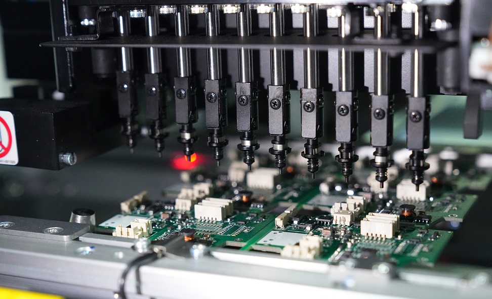
3. Preparation of pick and place equipment: According to the production scale and accuracy requirements, select the appropriate mounting machine, and ensure that the working parameters of the mounting machine (such as nozzle height, mounting pressure, mounting speed, etc.) have been correctly set.
4. Component pretreatment: For some special components, such as QFP (Quad Flat Package), BGA (Ball Grid Array), etc., it may be necessary to pre-treat, such as baking to remove moisture, to improve the reliability of mounting.
5. Solder paste printing
- Fixes the stencil onto PCB board to ensure stencil and PCB board is tight and there is no gap.
- Evenly printing the solder paste onto the pad of the wireless PCB board. The thickness and shape of the solder paste should meet the process requirements, which are generally controlled by adjusting the pressure, speed and angle of the scraper of the printer.
- After the printing is completed, use a microscope or automatic optical inspection equipment (AOI) to check the quality of the solder paste printing, such as whether the solder paste amount is uniform.
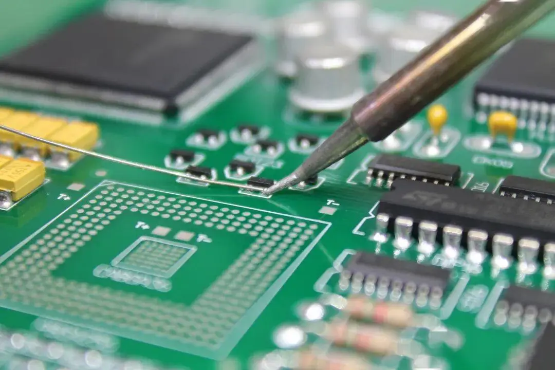
6. Pick and place assembly
In the mounting process, pay attention to the direction and position accuracy of the components, especially for some small components and small pin spacing Package forms, such as 0402, 0201 patch resistance capacitor and QFN (Quad Flat no-leads Package, square Flat No pin package). For some larger or heavier components, it may be necessary to increase mounting pressure or use special mounting methods to ensure good contact between the component and the pad.
7. Reflow welding: The PCB board with the installed components is fed into the reflow welder. The reflow welder melts the solder paste through heating, forming a good solder spot, and solidly welds the components on the PCB board.
8. Cleaning and testing: For applications that require high cleanliness, such as medical devices and aerospace, it may be necessary to clean the welded PCB board to remove residual flux and impurities. The cleaning method can be water cleaning, solvent cleaning or ultrasonic cleaning, etc. The specific cleaning process should be selected according to the material, component type and cleaning requirements of the PCB board.
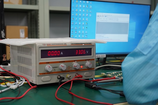
9. Finally, the wireless PCB board for comprehensive functional testing and performance testing, including wireless communication function testing, electrical performance testing, reliability testing. Ensure that the wireless PCB board meets the design requirements and product standards, can work properly and operate stably and reliably.
If you want know more about wireless PCB or PCB assembly, welcome to contact us at sales@bestpcbs.com. Our technical team are always online!