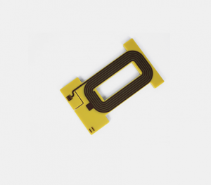
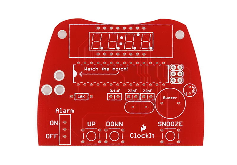
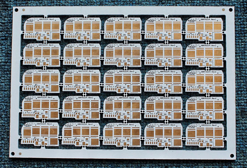
In PCB manufacturing, the amount of gold in circuit boards is usually described by gold plating thickness, not by weight. For common ENIG surface finish, the immersion gold layer is typically about 1–3 µin thick, equal to 0.025–0.075 µm. For gold fingers, edge connectors, RAM contacts, and high-reliability plug-in areas, the gold is usually thicker, often around 15–30 µin, and some demanding designs may use 30–50 µin hard gold plating.
How Much Gold in Circuit Boards?
Do All Circuit Boards Have Gold?
Not all circuit boards have gold. Some do, some do not, and many contain only very small plated areas. Gold is usually applied only where the design needs stable contact performance, strong resistance to oxidation, or reliable signal transmission over time.
In practical PCB manufacturing, gold is not a default finish for every board. It is a selective engineering choice. Low-cost consumer products often use finishes such as HASL, OSP, immersion tin, or immersion silver instead. These options are cheaper and work well enough for many standard applications.
Gold is most commonly found in:
- edge connectors
- card fingers
- switch contacts
- socket interfaces
- high-reliability contact pads
- wire bonding areas in certain semiconductor packages
So, if someone asks, “Do all circuit boards have gold?” the best answer is simple: no, but many important electronic assemblies use gold in specific functional locations.
Is There Real Gold in Circuit Boards or Just Gold-Colored Coating?
Yes, the gold used in electronics is real gold. In most cases, however, it is a very thin plated layer rather than a thick deposit or solid piece of metal.
This distinction matters. When people see bright yellow connector fingers on a RAM module or motherboard slot, they often imagine a large amount of recoverable precious metal. In reality, that visible gold surface is usually only a thin functional coating applied over nickel. The nickel acts as a barrier and structural layer. The gold provides a clean, oxidation-resistant surface with excellent conductivity.
Common PCB-related gold finishes include:
| Gold Finish Type | Typical Use | Why It Is Used | Value for Recovery |
|---|---|---|---|
| ENIG | PCB pads and solderable surfaces | Flatness, solderability, corrosion resistance | Low |
| Hard Gold | Edge connectors, contact fingers | Wear resistance, repeated insertion cycles | Medium |
| Gold Bonding Surfaces | Semiconductor packaging | High-reliability interconnection | Higher |
| Thick Gold in Legacy Parts | Older CPUs and telecom hardware | Long-term durability | Higher |
So the answer is not “fake gold” versus “real gold.” It is usually real gold, but used in very small engineered quantities.
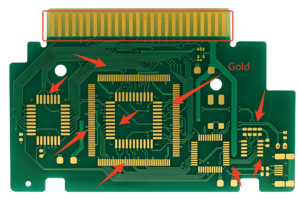
Where Is Gold Usually Found on a Circuit Board?
Gold is typically found in the places where contact quality matters most. That means it is not spread evenly across the whole board. It is concentrated in small functional areas.
The most common gold-bearing PCB areas include:
- connector fingers on memory modules and add-in cards
- contact pads in sockets and plug-in interfaces
- plated contacts in telecom and server boards
- switch contacts in precision electronics
- bonding pads in hybrid or semiconductor assemblies
A typical motherboard may have gold in the PCIe slots, RAM slot contacts, CPU socket areas, and selected chip connections. A standard low-cost appliance control board may have almost none.
How to Identify Gold in Electronics Without Guessing?
The fastest way to identify likely gold-bearing parts is visual inspection, but visual inspection alone is not enough for a confident conclusion. Gold color can be misleading. Some finishes look similar even when no gold is present.
A practical identification approach starts with observation:
- bright yellow metallic finish
- smooth, uniform contact surfaces
- no obvious tarnishing
- presence on connector fingers or high-contact pads
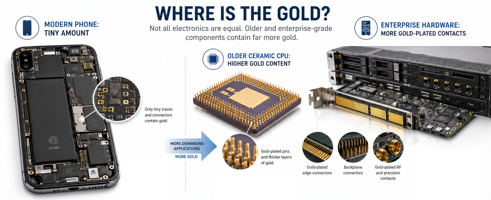
Which Electronics Contain the Most Gold?
Not all electronics contain the same amount of gold. Older high-reliability components and legacy computer hardware often contain much more gold than modern low-cost consumer devices.
The general rule is simple: the more demanding the electrical contact requirement, the more likely gold is used.
Here is a clear comparison:
| Electronic Part | Relative Gold Content | Typical Gold Location | Recovery Potential |
|---|---|---|---|
| Ceramic CPU | Very High | Internal bonding wires, lids, pins | High |
| Older telecom boards | High | Connectors, contact arrays, plated interfaces | High |
| Server RAM | Medium to High | Gold fingers | Medium |
| Desktop motherboard | Medium | Slots, sockets, contacts | Medium |
| Smartphone PCB | Low | Small contact pads, connectors | Low |
| SIM card | Very Low | Surface contacts | Very Low |
Many people assume phones are full of gold because they are advanced devices. In reality, each phone contains only a tiny amount. By contrast, older ceramic CPUs and enterprise hardware often contain more concentrated gold and are therefore more attractive to recyclers.
Does Computer Motherboard Have Gold?
Yes, computer motherboards do contain gold, but not in the dramatic amounts often suggested online. The gold is real, yet it is spread across small functional locations and usually exists as thin plating.
Typical motherboard gold locations include:
- CPU socket contacts
- RAM slots
- PCIe and expansion slot connectors
- selected chip contact pads
- internal interface terminals
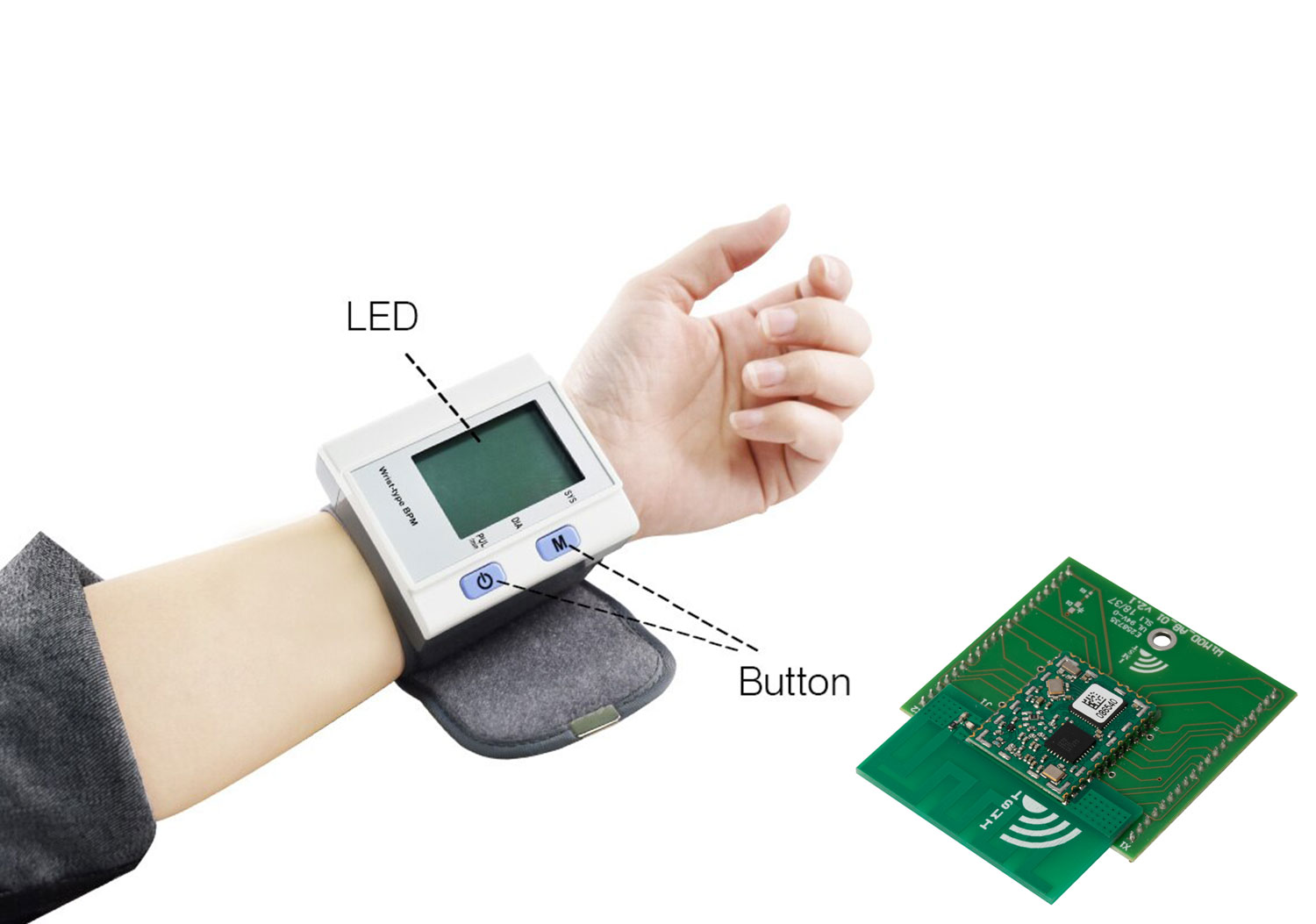
Gold is used in these locations because motherboards handle high-speed signals and repeated contact cycles. Oxidation on these surfaces can affect electrical performance, especially over time.
So the most accurate answer is: yes, motherboards have gold, but the amount per board is modest and the value depends heavily on board type, age, and hardware class.
Are the Gold Contacts on SIM Cards Really Gold?
Yes, the gold contacts on SIM cards are usually real gold plating. The layer is extremely thin, but it is used for a real purpose.
SIM card contacts need to maintain stable electrical contact over repeated insertion and removal. They are also exposed to air, skin oils, and environmental contamination. Gold helps prevent oxidation and keeps the contact surface reliable.
However, from a recovery perspective, SIM cards are not attractive. The amount of gold is tiny. A single SIM card contains so little gold that it is not practical to recover unless it is processed in very large industrial volumes.
This is a good example of a key principle in electronics: gold is often used because it works well, not because the product is meant to hold precious metal value.
What Is the Gold Content in Ceramic CPUs?
Ceramic CPUs are among the best-known gold-bearing electronic parts. This is one reason they attract so much attention from recyclers and collectors.
Older ceramic CPUs often contain gold in:
- internal bonding wires
- pin plating
- lid plating
- package interconnection structures
These parts were produced in an era when durability and performance often mattered more than aggressive cost reduction. As a result, the use of gold was less restrained than in modern consumer-grade packaging.
Modern plastic-packaged CPUs still contain gold in some internal structures, but the amount is usually lower. That is why ceramic CPUs are consistently seen as a higher-value electronic scrap category.
Still, “high gold content” is relative. Even ceramic CPUs do not contain huge masses of gold. They simply contain more than many modern components.
Why Is Gold Used in Circuit Boards Instead of Copper or Tin?
Gold is not used because it is luxurious. It is used because it solves real engineering problems that copper and tin cannot solve as well in exposed contact areas.
Copper is highly conductive, but it oxidizes easily. Oxidation raises contact resistance and can reduce reliability. Tin is affordable and solderable, but it does not provide the same stable long-term contact performance in all conditions.
Gold offers several advantages:
- excellent corrosion resistance
- low and stable contact resistance
- strong long-term reliability
- good performance in low-current signal interfaces
- stable behavior in harsh environments
This is why gold remains important in:
- medical electronics
- aerospace hardware
- industrial control systems
- telecom infrastructure
- server and data communication equipment
When reliability matters more than minimizing cents per unit, gold still earns its place.
How Much Gold Is Actually in Electronics?
The amount of gold in electronics is usually much smaller than people expect. Many discussions about “gold in circuit boards” confuse visibility with quantity. A gold-colored connector may look valuable, but the actual gold layer can be extremely thin.
Typical estimates vary by device and design, but the general pattern looks like this:
| Device Type | Typical Gold Presence | Practical Interpretation |
|---|---|---|
| Smartphone | Very small | Real gold exists, but in tiny amounts |
| Laptop | Small | More contact points than a phone, still limited |
| Desktop motherboard | Small to moderate | Depends on age and board grade |
| Server board | Moderate | Better connectors and higher reliability hardware |
| Ceramic CPU | Moderate to high relative to electronics | More concentrated gold-bearing structures |
The key point is this: electronics contain valuable gold because of concentration across many units, not because one board contains a dramatic amount.
That is why industrial-scale recycling works and casual small-batch recovery usually does not.
Why Do Most People Overestimate Gold in Electronics?
Most people overestimate gold in electronics because they confuse visible plating with total metal volume. The eye sees a bright gold surface and assumes there must be a thick layer underneath. In reality, most electronic gold is engineered to be just thick enough to perform its function.
There are three common misunderstandings:
1. Gold color means high gold value
Not true. Many visible gold surfaces are extremely thin.
2. Every motherboard is worth refining
Not true. Recovery economics depend on scale, hardware class, and process cost.
3. Modern electronics contain more gold because they are more advanced
Usually not. Modern products are often optimized to use less precious metal.
This misconception matters for content strategy too. Users are not only asking whether gold exists. They are really asking whether it exists in an amount that matters. That is why value, comparison, and practicality sections perform so well in search-focused content.
Is It Worth Getting Gold From Circuit Boards?
In most small-scale situations, recovering gold from circuit boards is not worth it. The chemistry, labor, safety equipment, and waste handling requirements usually cost more than the recovered gold is worth.
Industrial recovery is different. Large-scale recyclers can process high volumes, separate materials efficiently, and manage hazardous waste under controlled systems. Their economics are based on throughput, not curiosity.
For individuals or small workshops, the main issues are:
- very low yield per item
- chemical handling risk
- time-intensive separation work
- disposal and environmental compliance costs
So the honest answer is: gold recovery from circuit boards can be profitable at industrial scale, but it is rarely practical as a casual small-scale activity.
How Is Gold Extracted From Circuit Boards in Practice?
Gold extraction from electronics is a multi-step process, not a simple one-bottle trick. Professional recovery operations separate materials carefully before any chemical stage begins.
A simplified process usually includes:
1. Collection and sorting
High-value parts such as ceramic CPUs, connector-rich boards, and gold-finger scrap are separated from low-value material.
2. Mechanical disassembly
Boards are stripped, and selected gold-bearing components are isolated.
3. Pre-processing
Material may be shredded or prepared for further separation.
4. Chemical treatment
Industrial operators use controlled methods to dissolve and recover precious metals.
5. Refining and purification
Recovered metal is further processed to improve purity.
This is exactly why it is not a beginner-friendly task. The challenge is not simply “finding gold.” The challenge is separating a very small amount of gold from a large amount of base metal safely and economically.
What Safety Issues Matter When Recovering Gold From Electronics?
The biggest risk in gold recovery is not the low yield. It is the chemical hazard. Even small-scale experiments can expose people to dangerous fumes, corrosive liquids, and contaminated waste.
Major risks include:
- acid burns
- toxic gas release
- contaminated wastewater
- metal-bearing sludge disposal
- inhalation risk during stripping or heating
That is why responsible content should never glamorize extraction. It is better to explain the reality clearly: identifying gold in electronics is useful knowledge, but recovery should be approached as an industrial materials process, not a casual hobby project.
What Industries Still Use High-Gold PCBs Today?
Gold-plated PCBs remain essential in industries where electrical failure is expensive, dangerous, or unacceptable. These are not vanity applications. They are reliability-driven uses.
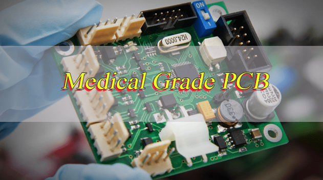
Medical equipment case
In medical electronics, stable contact performance matters because devices may operate continuously and support critical diagnosis or treatment. Gold plating is commonly used in interfaces where signal stability, corrosion resistance, and long service life matter.
Examples include:
- imaging system interface boards
- patient monitoring modules
- precision diagnostic control assemblies
Aerospace case
Aerospace systems face vibration, thermal cycling, and long-term exposure challenges. Contact degradation can become a serious reliability issue. Gold-plated connectors and high-reliability PCB finishes are therefore common in avionics and communication systems.
Examples include:
- flight control electronics
- satellite communication boards
- navigation and sensing modules
Industrial equipment case
Industrial control systems often run in harsh environments with dust, heat, vibration, or humidity. Gold plating improves long-term contact stability in systems that cannot afford intermittent signal issues.
Examples include:
- inverter control boards
- automation PLC interface cards
- high-reliability power distribution assemblies
These sectors show the real value of gold in electronics. It is not about appearance. It is about dependable function.
FAQ About Gold in Circuit Boards
1. Do all circuit boards have gold?
No. Gold is used selectively in connectors, contact pads, and high-reliability areas. Many low-cost boards do not use gold at all.
2. How can I identify gold in electronics?
Start with visual inspection of connector fingers and contact surfaces, then use XRF or material testing for confirmation.
3. Is the gold in circuit boards real gold?
Yes. In most cases it is real gold plating, but the thickness is usually very small.
4. Does computer motherboard have gold?
Yes. Gold is commonly found in slots, sockets, and selected contact points, though the amount is limited.
5. Are the gold contacts on SIM cards real gold?
Yes, but the layer is extremely thin and has very low recovery value.
6. Which electronics contain the most gold?
Older ceramic CPUs, telecom boards, and some server-grade components usually contain more gold than standard consumer devices.
7. Is it worth extracting gold from circuit boards?
Usually only at industrial scale. Small-scale recovery is rarely economical once labor, chemicals, and waste handling are considered.
8. Why is gold used in electronics at all?
Because it resists oxidation and provides stable, low-resistance electrical contact over long periods.
Need High-Reliability Gold-Plated PCBs for Your Product?
If your project needs dependable contact performance, stable signal transmission, and strong corrosion resistance, the plating choice should never be treated as a small detail. In medical, aerospace, and industrial electronics, surface finish quality directly affects reliability.
At EBest Circuit, we manufacture gold-plated PCBs for demanding applications, including ENIG and hard gold solutions with controlled process quality, traceability, and engineering support from prototype through production.
If you need this product or a related PCB solution, you are welcome to work with us. Our team can help review your design, recommend the right finish, and support fast, reliable manufacturing for your next project.