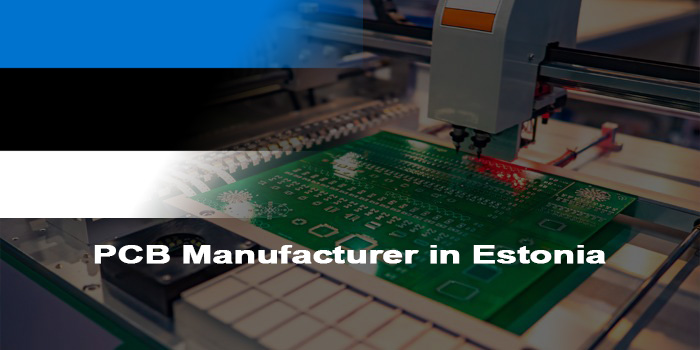
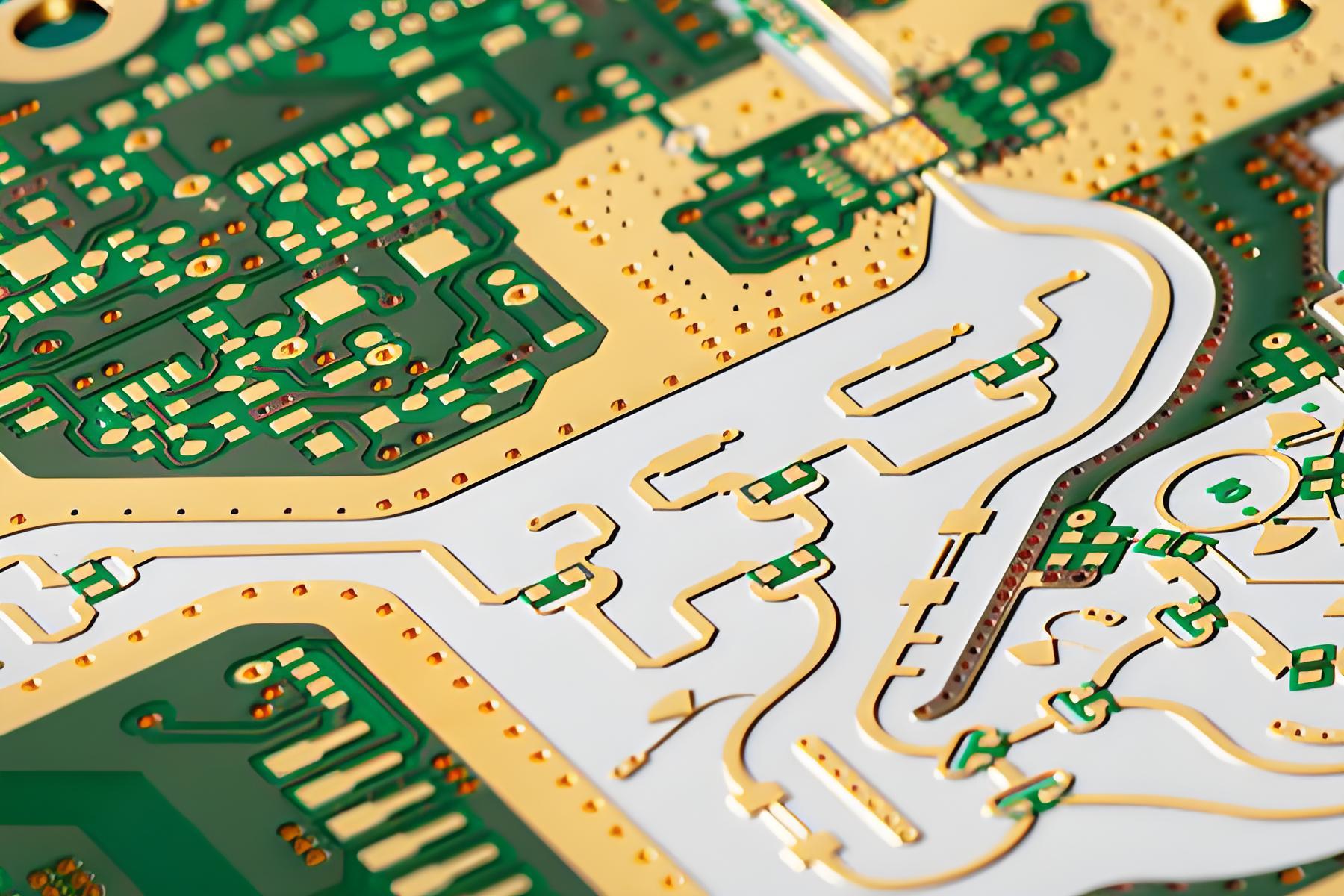
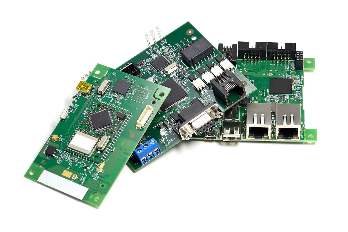
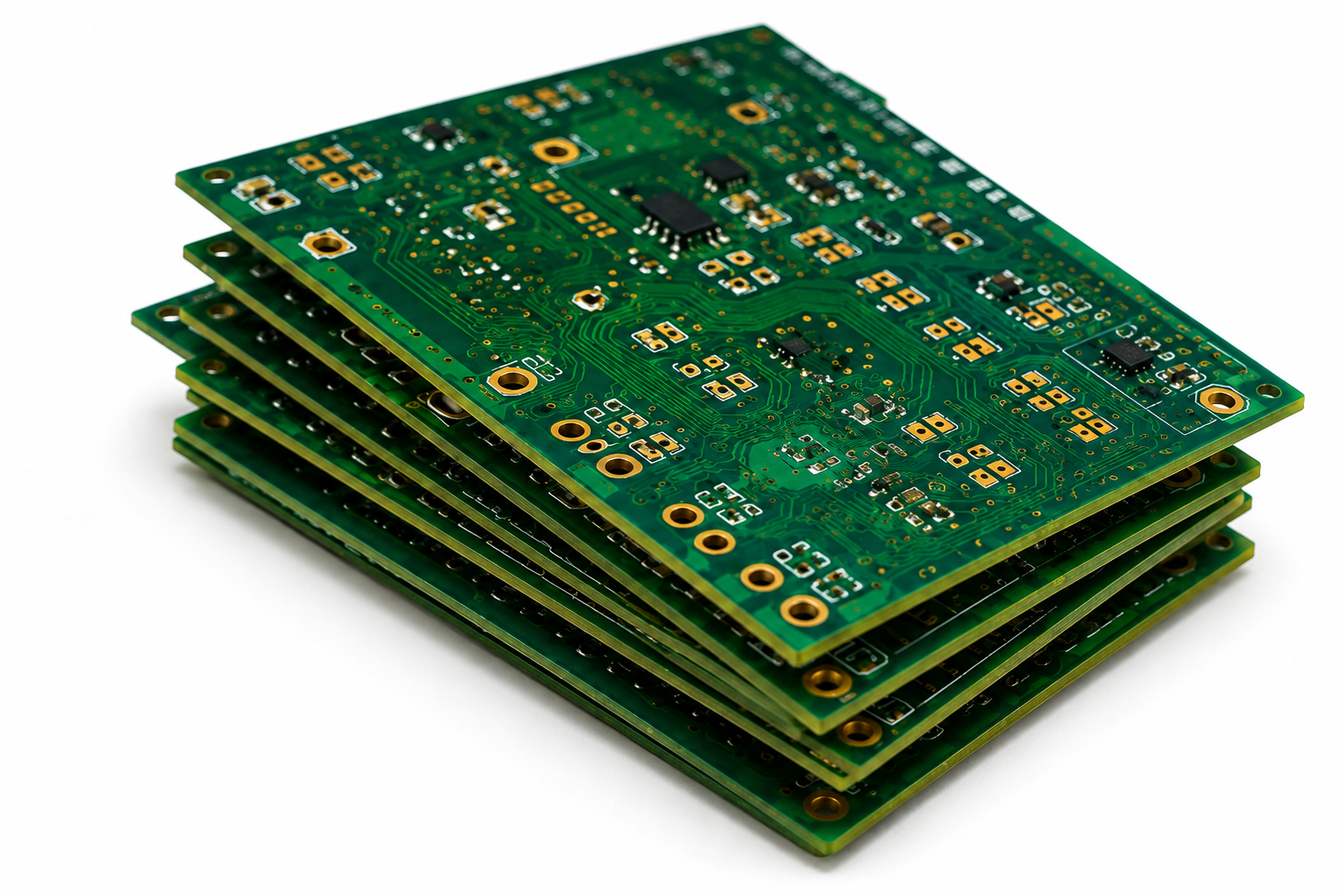
What is halogen free PCB, and why are more electronics manufacturers switching to it? As environmental regulations become stricter worldwide, halogen free PCB materials are increasingly used in automotive electronics, communication devices, LED lighting, industrial equipment, and medical products.
Traditional PCB materials often contain bromine and chlorine flame retardants. Under high temperatures or fire conditions, these substances may release toxic gases and dense smoke. Because of this, many manufacturers now prefer halogen free PCB solutions that provide safer environmental performance and better compliance with global standards.
A halogen free PCB not only supports cleaner manufacturing, but also improves product safety, thermal reliability, and long-term sustainability. Today, these materials are widely applied in high-reliability electronic products where stable performance is important.
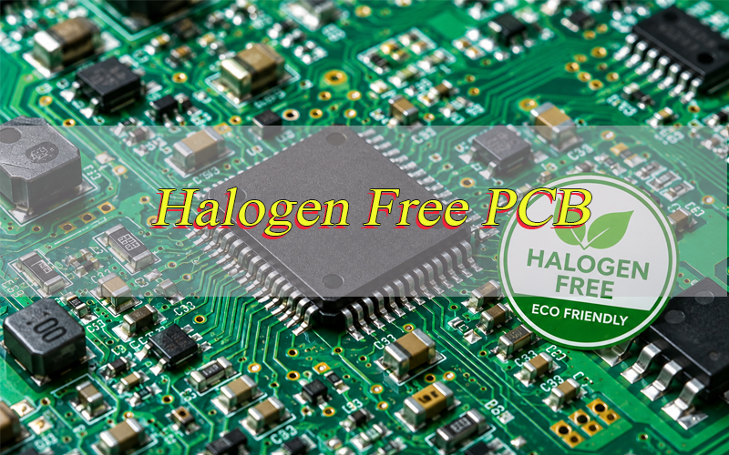
What is Halogen Free PCB?
What is halogen free PCB, and why are more electronic products using it today? Halogen free PCB refers to a PCB made without bromine or chlorine-based flame retardants. These materials help reduce toxic gas emissions during high-temperature conditions or fire exposure.
Traditional PCB materials often contain halogen compounds to improve flame resistance. However, when exposed to heat, these substances may release harmful smoke and corrosive gases. Because of this, many industries are shifting toward safer and more environmentally friendly PCB materials.
A halogen free PCB usually follows IEC 61249-2-21 standards. According to this specification:
- Chlorine content must remain below 900 ppm
- Bromine content must remain below 900 ppm
- Total halogen content must stay below 1500 ppm
Today, halogen free PCB products are widely used in automotive systems, industrial equipment, LED lighting, communication devices, and medical electronics because they support cleaner manufacturing practices and improved product safety.
Why Use Halogen Free PCB?
Why use halogen free PCB instead of traditional PCB materials? More manufacturers are choosing these materials because they support environmental compliance, product safety, and long-term reliability. Main advantages include:
- Reduce toxic smoke during overheating or fire exposure
- Lower environmental impact during disposal and recycling
- Meet RoHS and REACH environmental regulations
- Improve safety for enclosed electronic products
- Support sustainable manufacturing requirements
- Help exported products comply with international standards
- Provide stable thermal performance in demanding applications
Many industries now prefer halogen-free PCB materials because global environmental regulations continue becoming stricter every year.
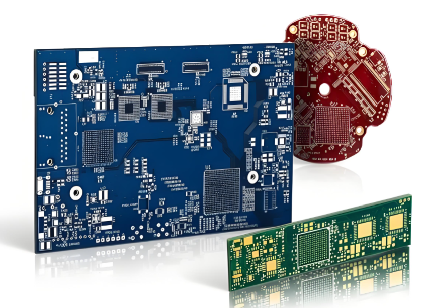
What Materials Are Used in Halogen Free PCB?
What materials are commonly used in halogen free PCB manufacturing? Most halogen free PCB products use specially developed resin systems and laminates designed to replace traditional brominated flame retardants. Common halogen free PCB laminate materials include:
- Halogen free FR4 epoxy resin
- Phosphorus-based flame-retardant systems
- Nitrogen compound resin systems
- Halogen-free CEM3 materials
- High Tg halogen-free laminates
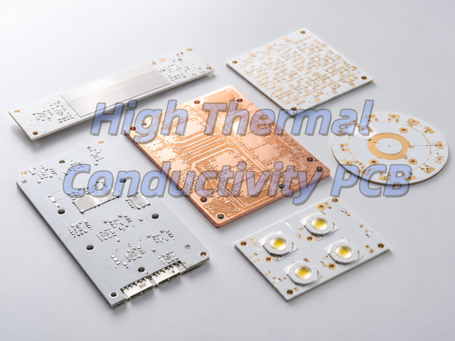
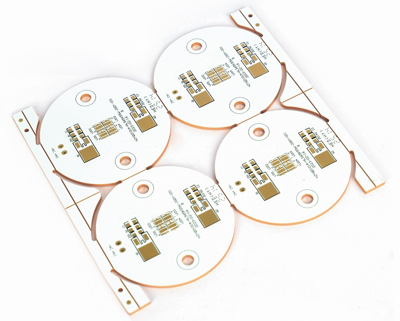
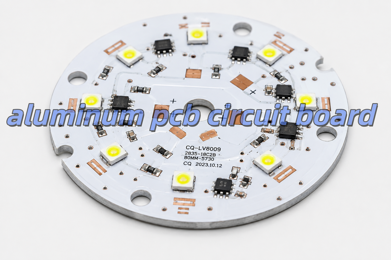
- Aluminum-based halogen-free materials
These materials maintain flame resistance while reducing hazardous substances. Many modern laminates also provide excellent thermal stability and reliable electrical insulation. Popular laminate manufacturers include:
- Shengyi
- ITEQ
- Panasonic
- Isola
- Rogers
High-quality halogen free PCB laminate materials are important for products exposed to high temperatures or continuous operation.
What Applications Use Halogen Free PCB?
Where is halogen free PCB commonly used today? These PCB products are now found across many industries because they combine environmental safety with stable electrical performance. Common applications include:
- Automotive control systems
- LED lighting modules
- Medical electronics
- Industrial automation devices
- Communication equipment
- Consumer electronics
- Power supply systems
- Renewable energy equipment
- Aerospace electronics
- Smart home products
Automotive and medical industries especially prefer halogen free PCB materials because these applications require high reliability, stable thermal performance, and environmental compliance.
What Are the Requirements for Halogen Free PCB?
What requirements must a halogen free PCB meet before being used in electronic products? Besides reducing harmful substances, the material must also provide stable thermal performance, reliable insulation, and environmental compliance. Main requirements for halogen free PCB include:
- Bromine content must be below 900 ppm
- Chlorine content must be below 900 ppm
- Total halogen content must be below 1500 ppm
- Must comply with IEC 61249-2-21 standards
- Must support RoHS and REACH environmental regulations
- Should meet UL94 V-0 flame-retardant standards
- Must provide stable thermal resistance during soldering
- Should maintain good electrical insulation performance
- Must have low moisture absorption
- Should support reliable multilayer lamination
- Surface finish compatibility should remain stable
- PCB materials should pass electrical and reliability testing
- Manufacturers should provide material traceability and certification reports
Many modern halogen free PCB materials also use high Tg resin systems to improve heat resistance and long-term reliability in automotive, industrial, LED, and communication applications.
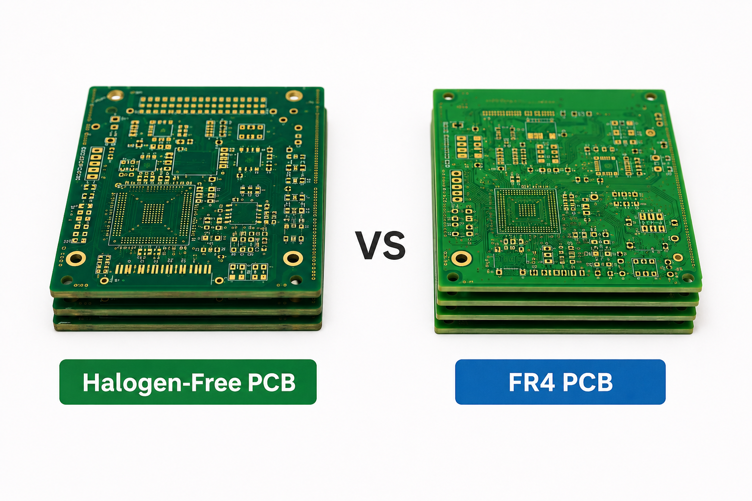
Halogen-Free PCB vs FR4 PCB: What is Difference?
What is the difference between halogen-free PCB and standard FR4 PCB? Both materials are widely used in electronics manufacturing, but they differ in flame-retardant systems, environmental performance, thermal stability, and application suitability.
| Feature | Halogen-Free PCB | Standard FR4 PCB |
|---|---|---|
| Flame Retardant Type | Phosphorus or nitrogen-based system | Brominated flame retardant system |
| Halogen Content | Very low or none | Contains bromine/chlorine compounds |
| Environmental Performance | More environmentally friendly | Standard environmental performance |
| Toxic Smoke During Burning | Lower smoke and gas emission | Higher toxic smoke emission |
| RoHS & REACH Compliance | Excellent compatibility | Usually compliant but depends on material |
| Thermal Stability | Higher in many grades | Standard thermal stability |
| Tg Performance | Often high Tg materials | Normal Tg or high Tg available |
| Electrical Insulation | Stable insulation performance | Good standard insulation |
| Moisture Resistance | Better in many laminate systems | Standard moisture resistance |
| Reliability in High Heat | Better for high-temperature environments | Suitable for general applications |
| Processing Difficulty | Slightly stricter process control | Easier standard processing |
| Material Cost | Slightly higher | Lower |
| Recycling & Disposal Safety | Safer and cleaner | Moderate |
| Typical Applications | Automotive, medical, LED, industrial control | Consumer electronics, standard electronics |
| Market Trend | Growing rapidly | Traditional mainstream material |
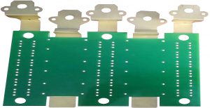
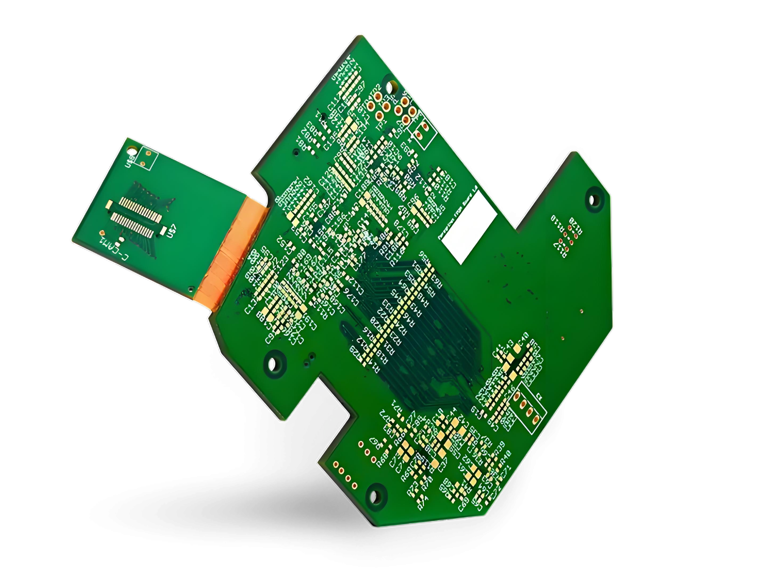
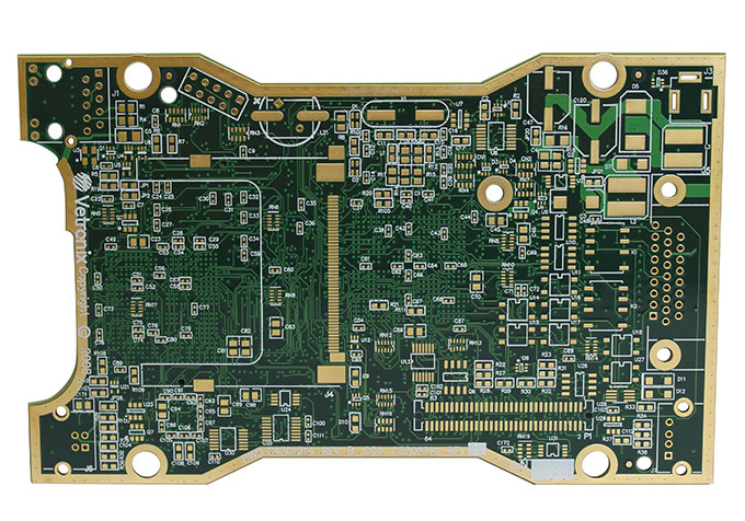
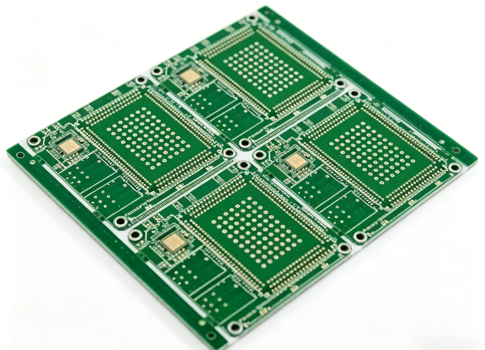
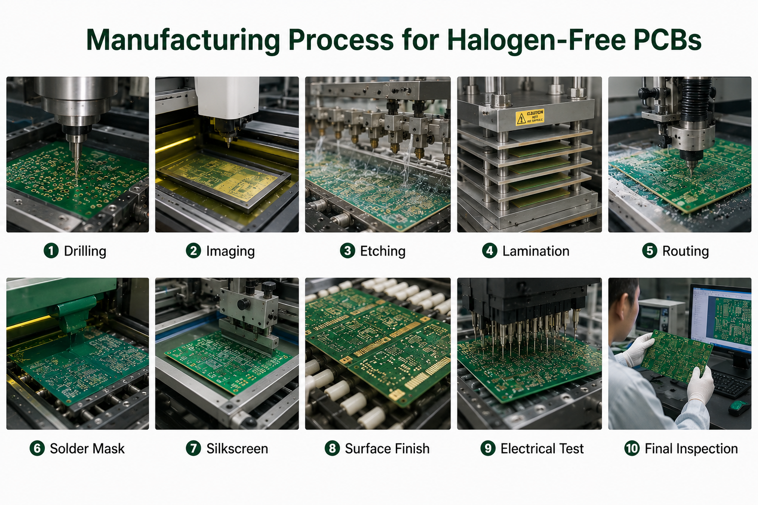
What is the Manufacturing Process for Halogen-Free PCB?
How are halogen-free PCBs manufactured? The basic process is similar to standard PCB production, but material selection, lamination control, drilling quality, and testing require closer attention because halogen-free laminates use different resin systems.
1. Material Selection
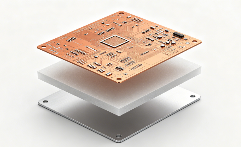
The manufacturer first selects suitable halogen-free PCB laminate according to the product application, layer count, Tg value, copper thickness, thermal demand, and compliance requirements. Common options include halogen-free FR4, high Tg laminate, CEM3 material, and aluminum-based material.
2. Material Inspection
Before production, the laminate, prepreg, and copper foil are checked for thickness, surface quality, certification, and halogen content report. This step helps ensure the material meets IEC 61249-2-21, RoHS, REACH, and project requirements.
3. Inner Layer Imaging
For multilayer PCBs, the inner copper layers are coated with dry film and exposed according to the circuit pattern. This step defines the inner layer traces and prepares the board for etching.
4. Etching and Inner Layer Inspection
Unwanted copper is removed to form the required circuit pattern. After etching, the inner layers are inspected for open circuits, short circuits, line width, spacing, and copper residue.
5. Lamination
The inner layers, prepreg, and copper foil are stacked together and laminated under controlled temperature and pressure. Halogen-free materials may need adjusted lamination parameters because their resin flow and curing behavior can differ from standard FR4.
6. Drilling
Mechanical or laser drilling is used to create through holes, blind vias, buried vias, or microvias. Drilling quality is important because poor hole walls can affect copper plating and long-term reliability.
7. Desmear and Hole Metallization
After drilling, resin smear inside the holes is removed. Then the hole walls are chemically treated and plated with copper to build electrical connections between layers.
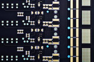
8. Outer Layer Imaging and Etching
The outer layer circuit pattern is created through imaging, plating, and etching. This step forms the final copper traces, pads, and connection areas on the PCB surface.
9. Solder Mask Application
A solder mask is applied to protect the copper surface, prevent solder bridging, and improve insulation. The solder mask must be compatible with halogen-free PCB material and assembly temperatures.
10. Surface Finish
A surface finish is added to protect exposed copper pads and improve solderability. Common options include ENIG, HASL, immersion silver, immersion tin, and OSP.
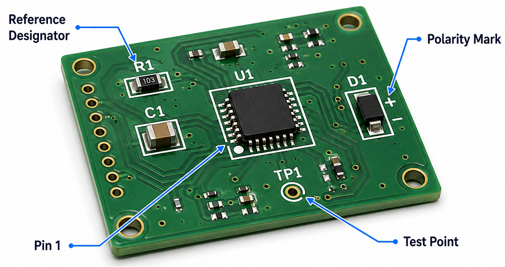
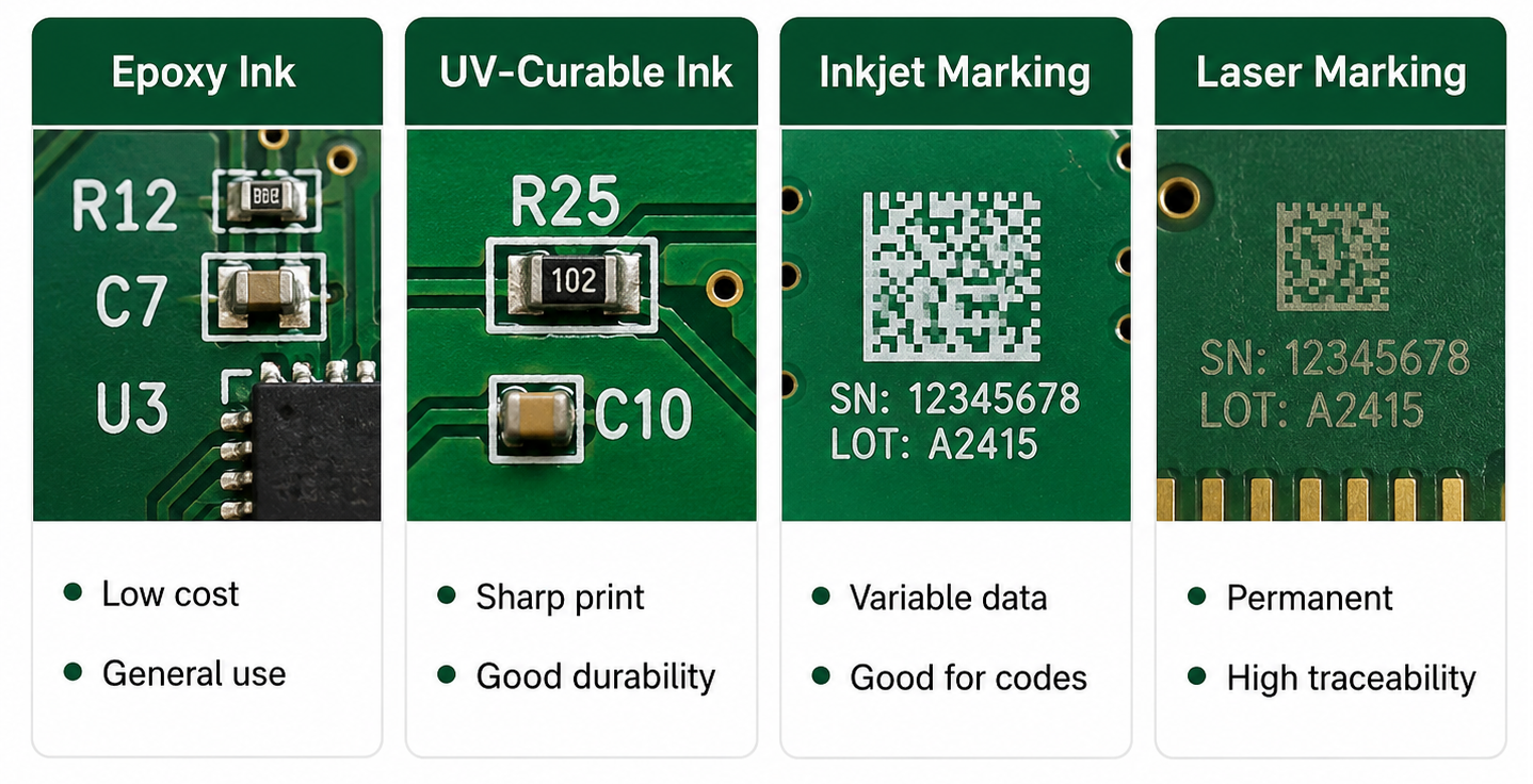
11. Legend Printing
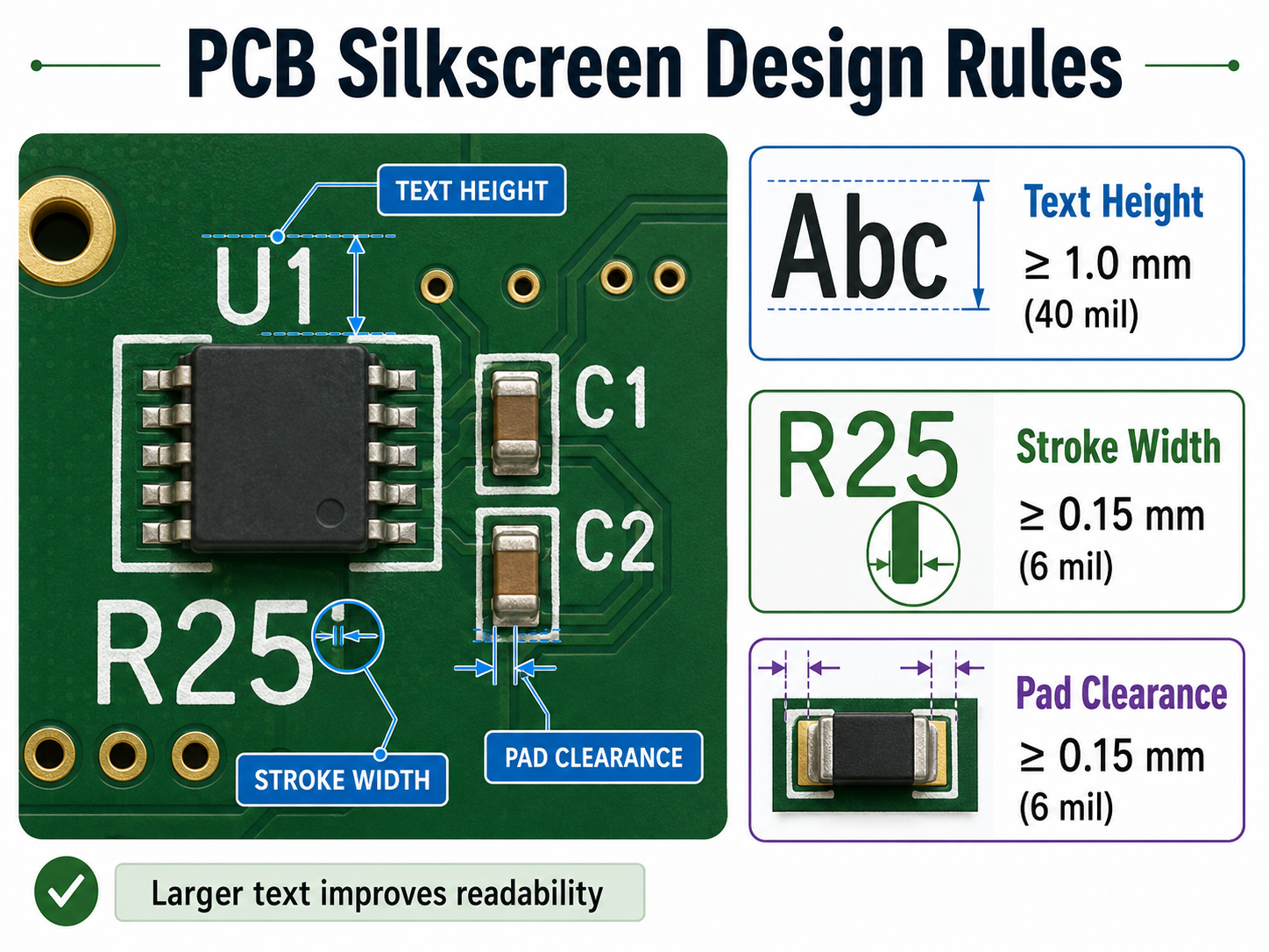
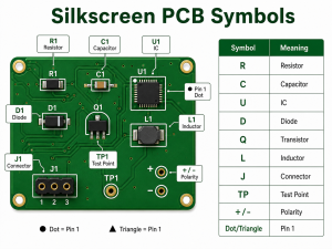
Component marks, logos, polarity symbols, and part numbers are printed on the PCB surface. This helps assembly teams identify placement direction and board information clearly.
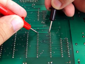
12. Electrical Testing
Each PCB is tested for open circuits, short circuits, and connection accuracy. This step helps confirm that the board matches the design files before shipment.
13. Reliability and Quality Inspection
The PCB may go through visual inspection, AOI, impedance testing, solderability testing, thermal stress testing, and dimensional inspection. For high-reliability applications, extra checks can be added based on project requirements.
14. Final Cleaning and Packaging
After inspection, the boards are cleaned, dried, vacuum packed, and labeled. Proper packaging helps prevent oxidation, moisture absorption, and surface contamination during storage and shipping.
Why Choose EBest for Halogen Free PCB Manufacturer?
Why choose EBest for halogen free PCB manufacturing? EBest Circuit has more than 20 years of PCB manufacturing experience and provides one-stop PCB solutions for global electronics industries.
EBest supports FR4 PCB, metal core PCB, ceramic PCB, RF PCB, high Tg PCB, HDI PCB, heavy copper PCB, and impedance control PCB manufacturing. Choosing EBest can bring the following advantages to your PCB projects:
- Stable halogen-free PCB material sourcing helps improve long-term product consistency
- High Tg laminate support improves thermal reliability in demanding applications
- One-stop PCB fabrication and assembly services help reduce supplier management costs
- PCB prototype and mass production support help shorten project development cycles
- Fast-turn production service helps reduce urgent project lead time pressure
- Some prototype orders can be shipped within 24 hours
- Monthly production capability reaching 260,000 square feet
- Strict quality inspection helps reduce manufacturing defects and reliability risks
- Electrical testing and reliability verification help improve product stability
- Support for multilayer and complex PCB structures helps simplify difficult projects
- Automotive, industrial, and medical manufacturing experience helps support high-reliability applications
- Support for RoHS, REACH, UL, ISO 9001:2015, ISO 13485:2016, IATF 16949, and AS9100D requirements
- Component sourcing and PCB assembly services help simplify supply chain management
- Stable international delivery capability helps improve project scheduling efficiency
From PCB prototype to mass production, EBest focuses on stable quality, fast response, and reliable manufacturing support for global electronics projects.
FAQs About Halogen Free PCB
Q1: Is halogen free PCB better than standard FR4 PCB?
A1: Halogen free PCB is often preferred for products that require better environmental performance, lower toxic emissions, and higher safety standards. Compared with traditional FR4 PCB, halogen-free materials can provide cleaner burning characteristics and stronger support for RoHS and REACH compliance.
Q2: Why are more electronic products using halogen free PCB?
A2: More electronic manufacturers are switching to halogen free PCB because environmental regulations are becoming stricter worldwide. Halogen-free materials help reduce harmful smoke, toxic gas emissions, and environmental impact during overheating or fire exposure.
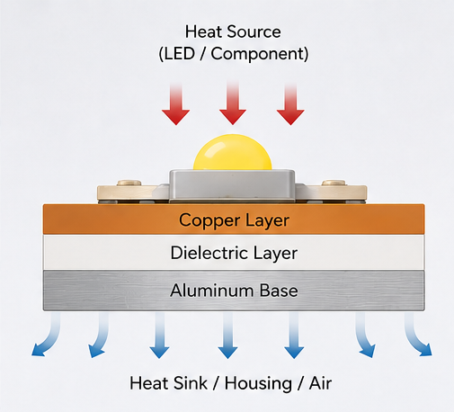
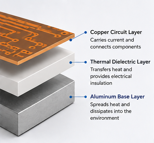
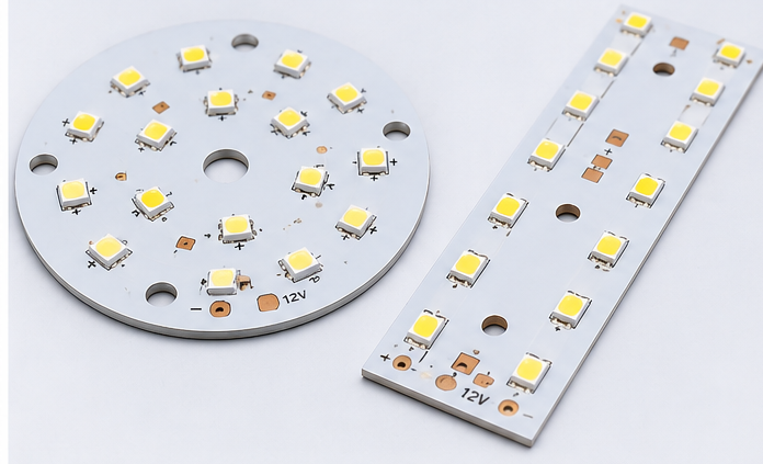
Q3: Can halogen free aluminum PCB be used in high-power products?
A3: Yes. Halogen free aluminum PCB is widely used in LED lighting, automotive lighting, power modules, and industrial power supplies because it combines environmental compliance with excellent heat dissipation performance.
Q4: Does halogen free PCB cost more than standard PCB?
A4: In many cases, halogen free PCB materials are slightly more expensive because of specialized resin systems and stricter manufacturing requirements. However, the improved thermal reliability, environmental performance, and global compliance advantages often make the additional cost worthwhile.
Q5: What industries commonly use halogen-free PCB materials?
A5: Halogen-free PCB materials are commonly used in automotive electronics, communication systems, medical devices, industrial automation equipment, LED lighting products, aerospace electronics, and renewable energy systems.
Q6: How can I identify a reliable halogen-free CEM3 PCB material supplier?
A6: A reliable supplier should provide certified material reports, stable laminate sourcing capability, strict quality inspection, and support for RoHS, REACH, and UL compliance standards.
Conclusion
EBest provides high-quality halogen free PCB manufacturing services for industrial, automotive, medical, communication, and LED applications. From PCB prototype to mass production, EBest supports reliable fabrication, stable material sourcing, and fast delivery services. Contact us today for your PCB project inquiry: sales@bestpcbs.com.