PCB vs. FPC is a common comparison when choosing the right type of circuit for modern devices. Both play important roles in electronics, but they serve different needs. To make the right choice, you need to know how they work, their uses, and their unique benefits.
In this blog, we’ll cover PCB vs. FPC in detail. We’ll also explore their antennas, pros, cons, and key applications. By the end, you’ll know which one fits your needs best.
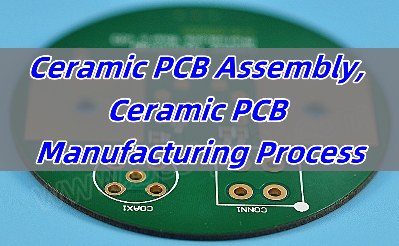
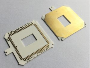
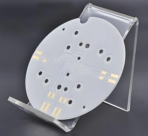
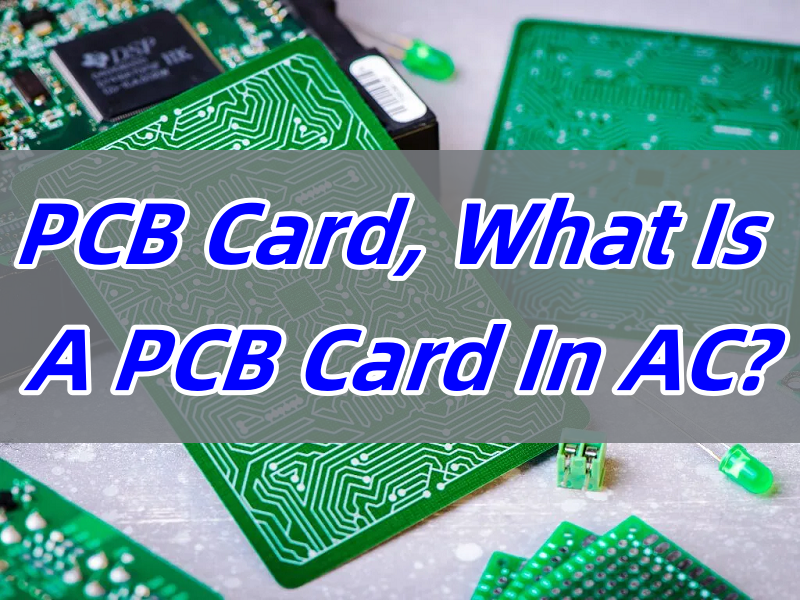
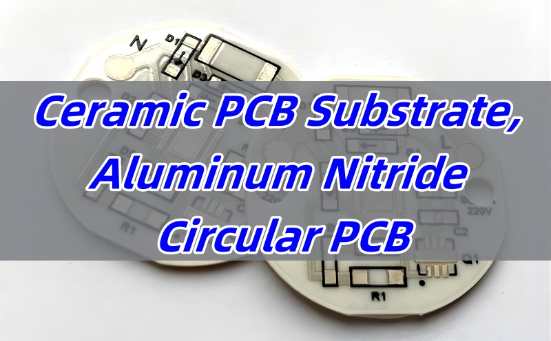
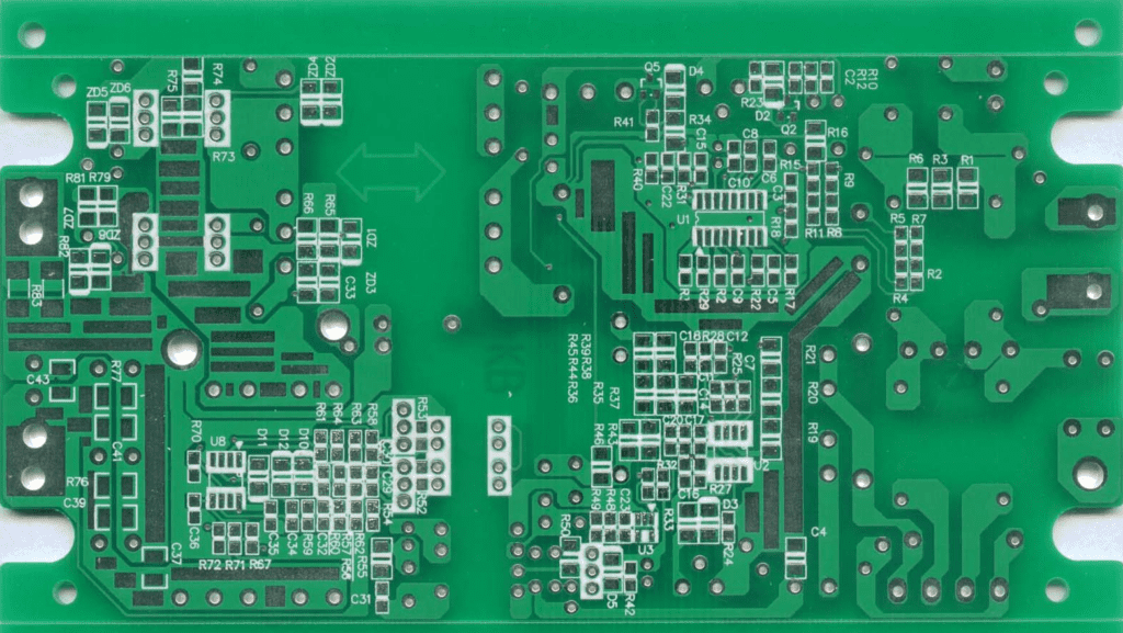
What is PCB and types of PCB?
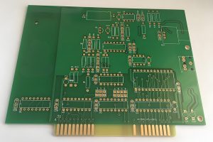
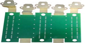
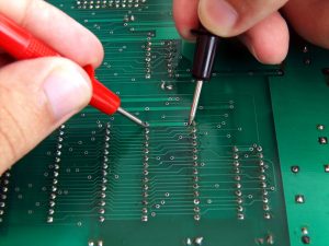
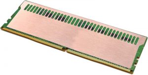
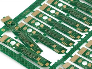
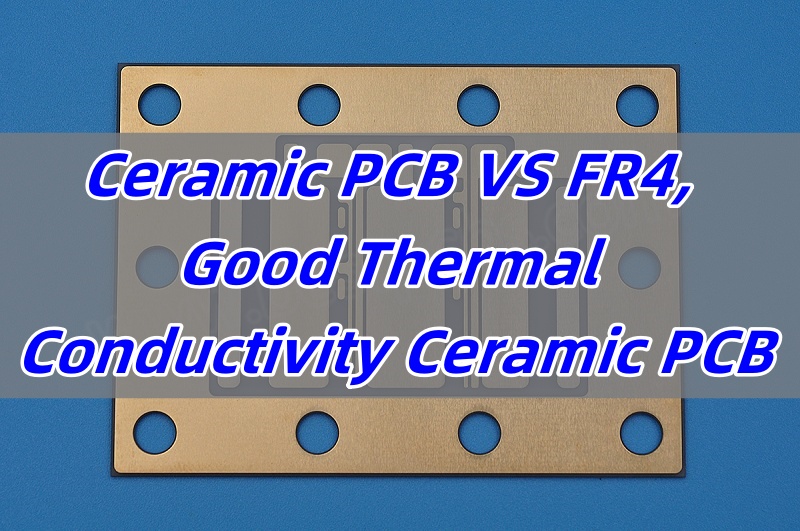
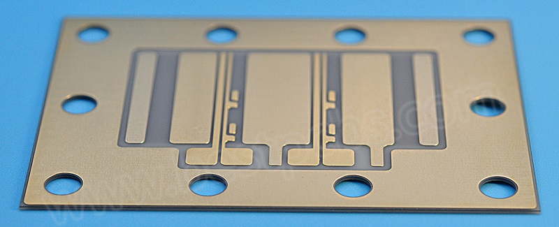
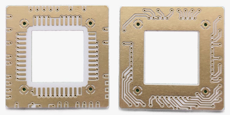
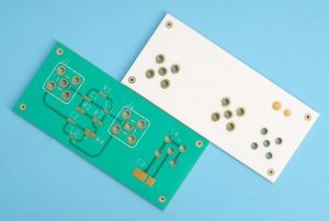
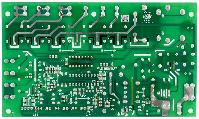
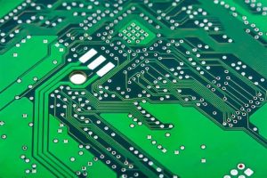
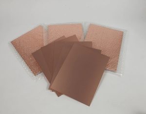
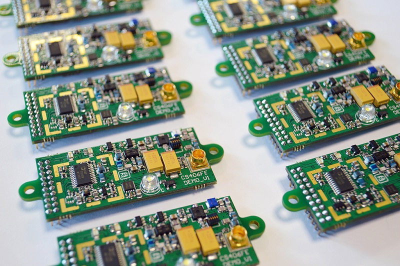
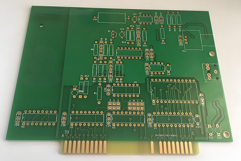
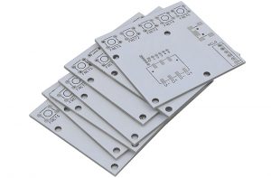
PCB stands for printed circuit board. It’s the most common type of circuit used in electronics. It supports components, connects them, and helps power flow correctly. Most devices today use PCBs for stable performance.
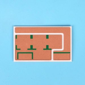
There are several types of PCBs, each suited for different tasks. Single-sided PCBs are the simplest. They have copper on one side and components on the other. These work well for simple products like toys or remotes.
Double-sided PCBs are a bit more complex. They have copper on both sides, which allows more connections. These are often used in home appliances and automotive parts.
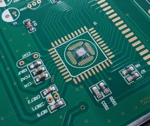
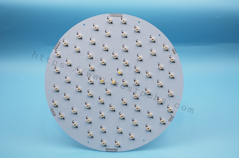
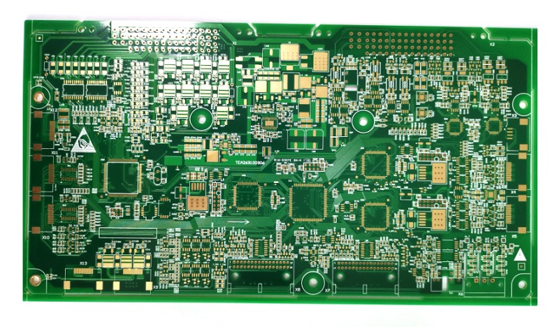
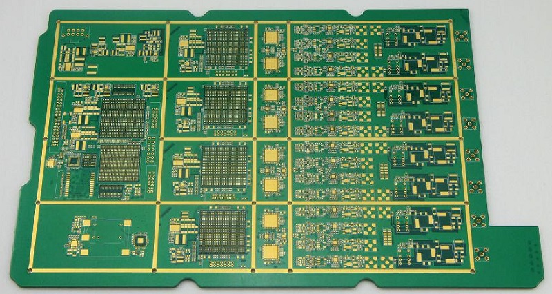
Multilayer PCBs are more advanced. They have multiple layers of copper and insulating materials stacked together. These can handle complex circuits found in computers, medical devices, and industrial equipment.
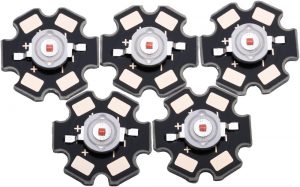
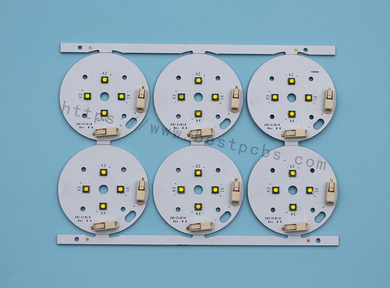
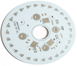
There are also special types like rigid PCBs, flexible PCBs, and metal core PCBs, each with its own role.
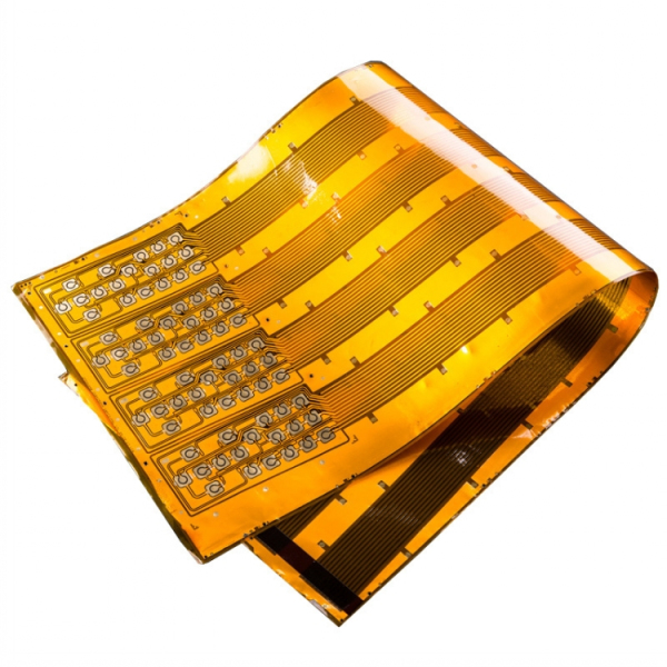
What is FPC in electronics?
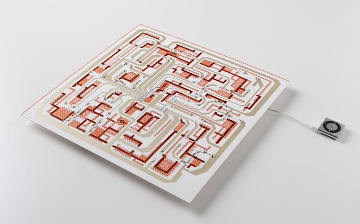
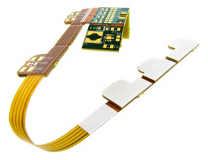
FPC stands for flexible printed circuit. As the name says, this type bends and twists. It’s made from flexible materials like polyimide, which handles bending without breaking.
Unlike standard boards, FPC circuits fit into tight spaces. This flexibility helps when devices need smaller, lighter, or more compact designs.
FPC technology has grown fast. Modern devices like wearables, foldable phones, and medical tools rely on it. Flexible circuits work well when regular boards are too stiff or bulky.
What is FPC used for?
FPC works well in devices where space is limited or flexibility is important. Wearables like smartwatches need circuits that bend with straps or bodies. FPC handles these shapes with ease.
Medical tools also benefit from FPC. Catheters, imaging devices, and hearing aids all use flexible circuits. They fit into tiny spaces without adding weight or bulk.
Cameras also rely on FPC. In phones and professional cameras, sensors need flexible connections to boards. FPC helps without taking up much room.
Automotive uses have also increased. Inside modern cars, FPC helps with touchscreens, sensors, and advanced controls. These circuits handle vibration and movement better than standard boards.
FPC can also be found in robotics, aerospace, and industrial tools where size, weight, and movement all matter.
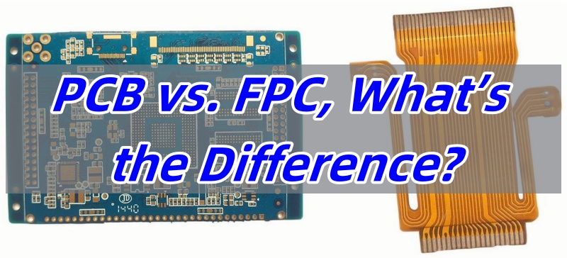
What is the difference between PCB and FPC?
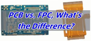
PCB vs. FPC, What’s the Difference? The biggest difference in PCB vs. FPC comes from flexibility. Regular PCBs are rigid, while FPC bends. This difference impacts how they are used.
PCBs offer strong support for larger, heavier components. They are better for devices with fixed shapes and stable housings. FPC, on the other hand, fits into flexible, curved, or moving parts.
Weight is another difference. Flexible circuits are much lighter than rigid boards. In lightweight products, FPC saves weight without losing performance.
FPC also reduces assembly steps. It often combines several rigid boards into one flexible piece. This simplifies connections and reduces assembly time.
Cost also varies. In low volumes, FPC usually costs more. However, for complex designs or space-saving needs, the benefits outweigh the cost.
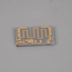
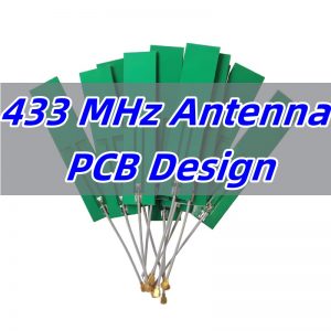
What is the difference between PCB antenna and FPC antenna?
PCB vs. FPC antennas is another important point. Both types support wireless signals, but they work differently.
PCB antennas are etched directly onto rigid boards. These antennas work well when space is not a big issue. They are sturdy and stable, making them reliable in stable devices like routers.
FPC antennas are flexible and thin. They fit into places where rigid antennas can’t. Wearables, smartphones, and small IoT devices often need FPC antennas to save space.
Performance-wise, both can offer good signal strength when designed well. However, FPC antennas handle curved surfaces better, while PCB antennas provide solid support in fixed devices.
What are the benefits of PCB?
PCB brings many benefits to electronics. First, it provides a stable base for components. This helps circuits perform reliably over time.
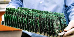
PCBs are also cost-effective for mass production. Automated assembly lines handle PCBs quickly, reducing labor costs.
Another benefit is versatility. From simple toys to complex industrial machines, PCBs adapt to all needs. They also handle higher power better than flexible boards.
PCBs also support many materials. Designers can choose materials to match heat, weight, and performance needs. This flexibility helps meet different project demands.
Finally, PCBs allow high precision. Advanced processes make tiny traces and complex layouts possible. This helps meet the needs of modern devices.
What are the disadvantages of PCB?
Even though PCB works well in most cases, there are some limits. One key point is lack of flexibility. Once installed, PCBs can’t bend or move.
Another drawback is weight. Compared to flexible circuits, PCBs are heavier. In portable devices, this can be a concern.
Size can also be a problem. In ultra-compact designs, rigid boards take up more space than flexible ones.
Finally, in very high-frequency designs, signal loss may occur if materials or layouts are not perfect.
What are the advantages of FPC?
FPC offers several valuable benefits. Flexibility comes first. It fits into small, curved, or moving spaces where rigid boards can’t go.
Weight savings is another advantage. Flexible circuits are much lighter than traditional boards. In wearables and aerospace tools, this is a big plus.
Space-saving design also stands out. FPC reduces or even removes the need for connectors and cables. This simplifies the design and reduces assembly time.
Durability adds value too. Properly designed FPC handles bending, vibration, and repeated flexing without damage. This helps in automotive, medical, and industrial tools.
Finally, FPC supports complex designs. It allows more creative shapes, which helps designers create smarter, smaller products.
What are the disadvantages of FPC?
Even though FPC offers many benefits, there are a few limits. Cost is one point. In low volumes, flexible circuits usually cost more than standard boards.
Handling can also be more delicate. Because of the flexible materials, FPC needs more care during assembly.
Repair can be harder too. Once damaged, FPC is more difficult to repair than regular boards.
In some high-power cases, FPC may not handle heat or current as well as thick rigid boards.
However, most of these points depend on design, material, and proper handling.
In a nutshell, when comparing PCB vs. FPC, the right choice depends on your project needs. PCB works well for stable, cost-effective designs where space is not too limited. It supports heavier parts and handles higher power easily.
On the other hand, FPC excels in compact, lightweight, and flexible designs. It’s the best fit for wearables, medical tools, and space-saving devices.
At EBest Circuit (Best Technology), we offer both high-quality PCB and FPC solutions. With over 18 years of experience, we help you choose the right option for your needs. Whether you need simple boards or advanced flexible circuits, our team delivers reliable, cost-effective solutions. If you have any questions or inquiries, don’t hesitate to reach out to us at sales@bestpcbs.com.