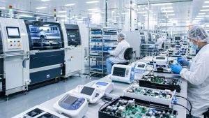
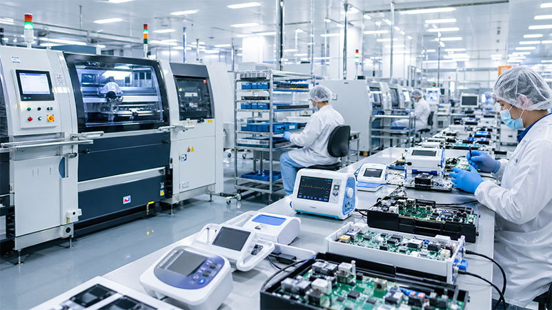
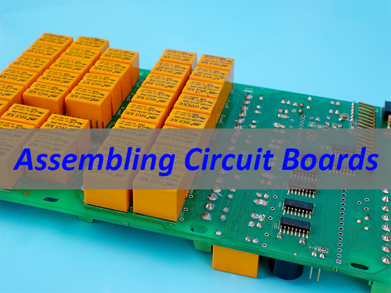
Assembling circuit boards is the step where a design becomes a real, working product. It sounds straightforward. In practice, it involves a precise chain of manufacturing steps — and a single weak link can mean failed boards, delayed launches, or expensive respins.
This guide walks through the full process. We cover what printed circuit board assembly actually involves, how each step works, what materials and finishes to choose, and how to avoid the mistakes that slow most projects down. We also explain what to look for when choosing a circuit board assembly service — and answer the questions engineers ask us most often.
What Is Assembling Circuit Boards (PCBA)?
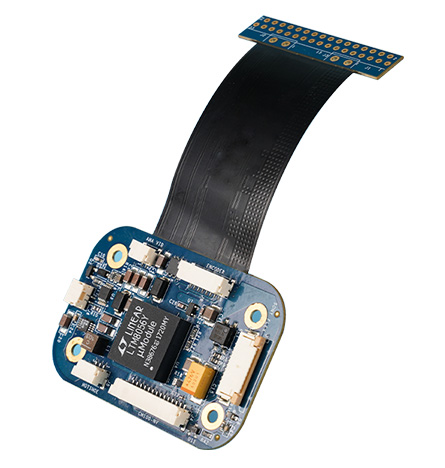
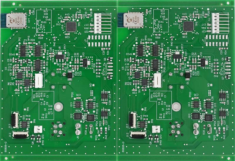
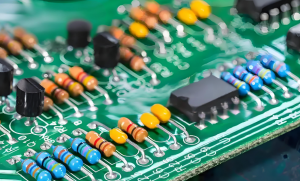
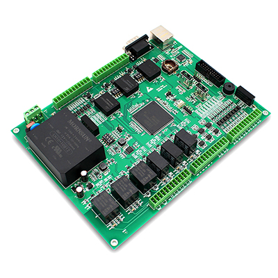
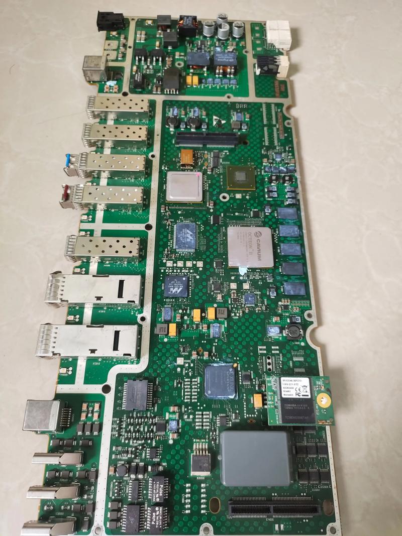
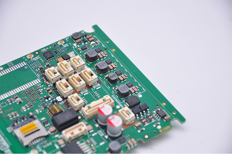
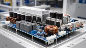
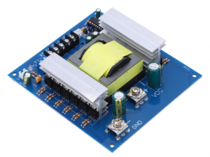
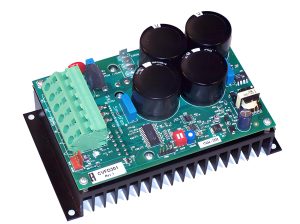
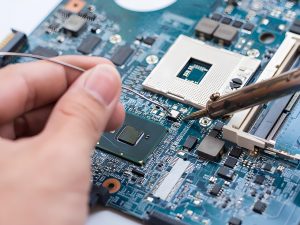
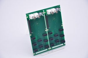
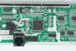
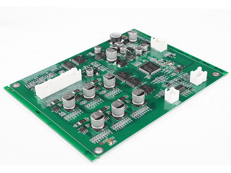
Assembling circuit boards — also called printed circuit board assembly, or PCBA — is the process of mounting and soldering electronic components onto a bare PCB. The result is a fully populated board that can be powered on and function inside a product.
However, the process involves more than just placing parts. It also includes solder paste printing, reflow soldering, through-hole insertion, automated inspection, X-ray checks for hidden joints, and functional testing. Each stage must be executed correctly. Because if one step fails, it affects every board in that batch.
It is also worth noting what PCBA does not include. It does not refer to bare PCB fabrication on its own. And it does not refer to chip-level semiconductor manufacturing. PCBA sits between those two — it is the assembly stage that turns fabricated boards and sourced components into working electronics.
PCB vs. PCBA: What Is the Difference?
Engineers sometimes use these terms interchangeably. In reality, they describe two different products at two different stages of manufacturing.
| Term | What It Is | What It Includes |
|---|---|---|
| PCB | Bare board | Copper traces, vias, pads, solder mask, silkscreen — no components |
| PCBA | Assembled board | PCB with all components soldered on, inspected, and tested |
| One-Stop Service | Full turnkey | PCB fabrication + BOM sourcing + SMT/THT assembly + testing, from one vendor |
The difference matters when sourcing. If you order a PCB, you still need to find an assembly house separately — and manage the handoff between them. In contrast, a one-stop circuit board assembly service handles fabrication, components, and assembly under one roof. This removes a common source of quality gaps and delays.
The Printed Circuit Board Assembly Process, Step by Step
Understanding the process helps engineers make better design decisions. Here is how a professional manufacturer works through each stage.
Step 1 — Engineering Review and DFM
Before anything is manufactured, the engineering team reviews your Gerber files, BOM, and assembly drawings. They look for issues that would cause problems in production — wrong pad sizes, missing clearances, risky component orientations. This review produces a DFM (Design for Manufacturing) report. Fixing problems at this stage takes hours. Fixing them after production starts takes weeks.
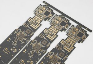
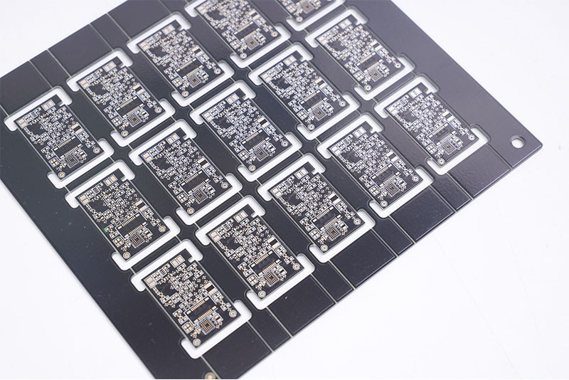
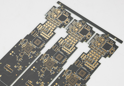
Step 2 — PCB Fabrication
The bare board is manufactured to spec. This means the correct layer stackup, copper weight, drill sizes, surface finish, and impedance control. Boards can range from single-layer to 50+ layers, depending on the circuit design.
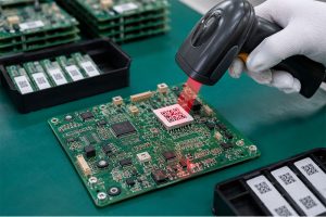
Step 3 — Component Sourcing and Incoming Inspection
All parts are procured from authorized distributors or verified suppliers. Before they go into assembly, incoming quality control checks markings, dimensions, and key electrical values. This step is the first line of defense against counterfeit components — a real and growing problem in the electronics supply chain.
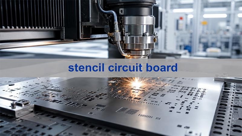
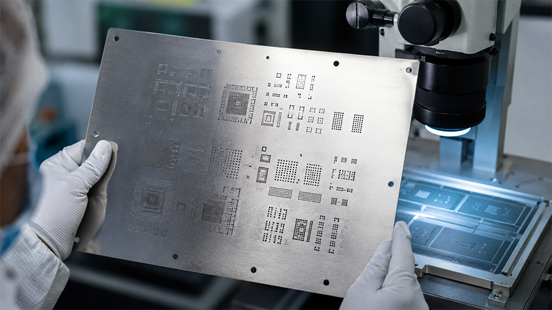
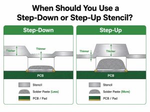
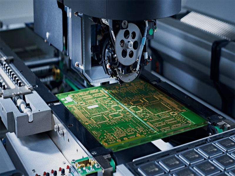
Step 4 — Solder Paste Printing
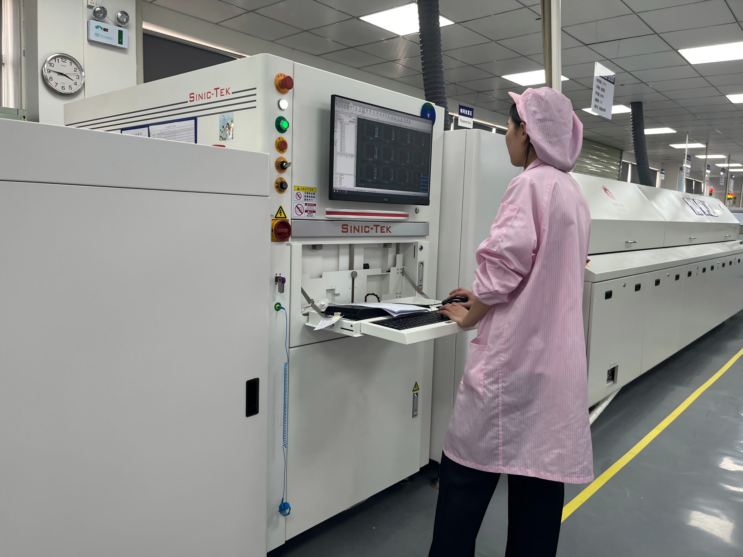
A stencil printer deposits solder paste onto the SMT pads. Too little paste causes cold joints. Too much causes bridging. After printing, automated solder paste inspection (SPI) checks every deposit before the board moves forward.
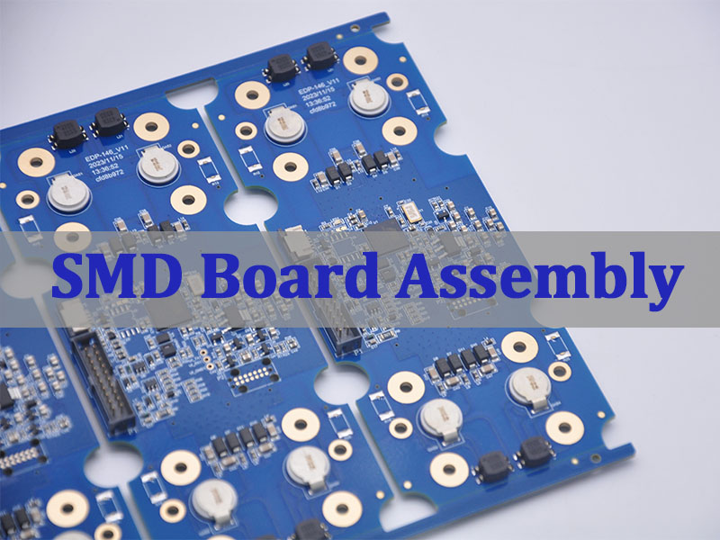
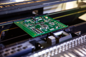
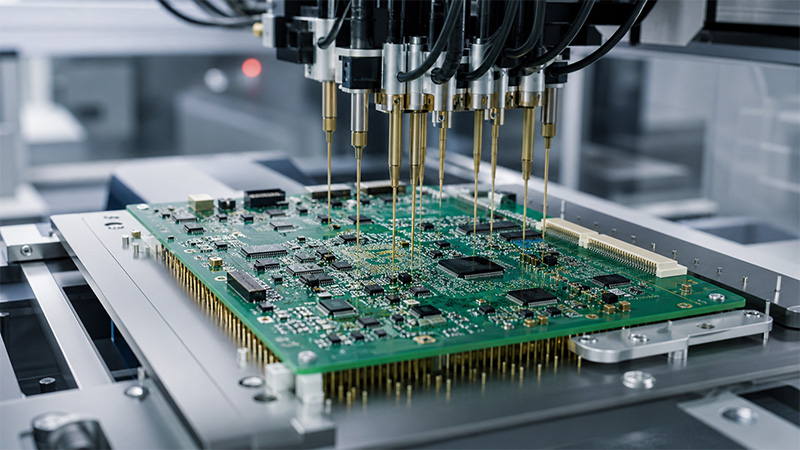
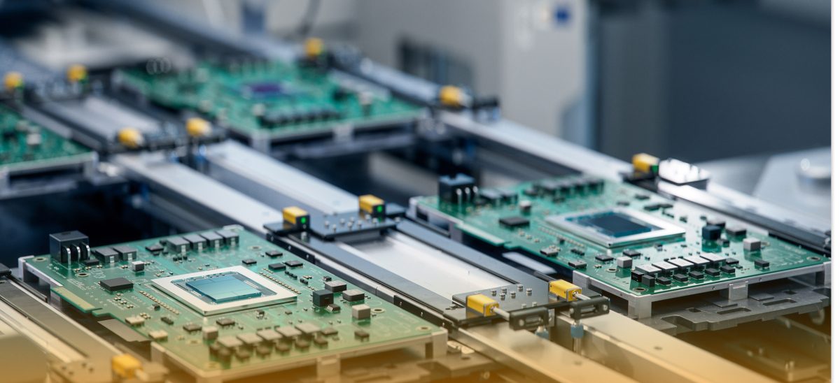
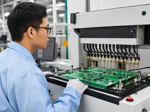
Step 5 — SMT Pick-and-Place
High-speed machines pick surface mount components — resistors, capacitors, ICs, BGAs, QFNs — and place them precisely on the solder paste. Modern equipment handles parts down to 01005 size (0.4 × 0.2 mm) with placement accuracy of ±0.025 mm.
Step 6 — Reflow Soldering
The populated board passes through a reflow oven. The temperature profile is controlled precisely so the solder paste melts and solidifies correctly. Profile design is especially important for lead-free soldering and for boards with high-Tg substrates.
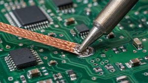
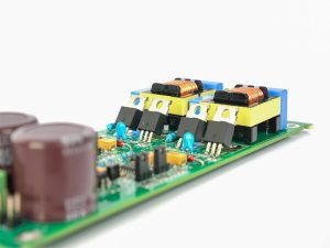
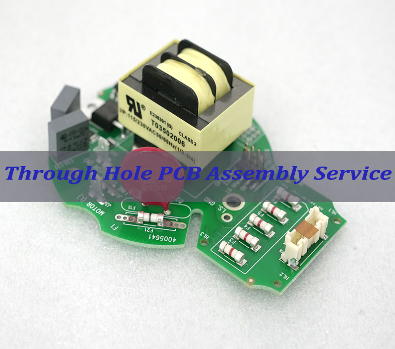
Step 7 — Through-Hole Assembly
Connectors, transformers, and other through-hole components are inserted next. Soldering is done by wave soldering or selective soldering, depending on the board layout. Selective soldering is preferred when SMT components are nearby and could be damaged by the heat of a full wave pass.
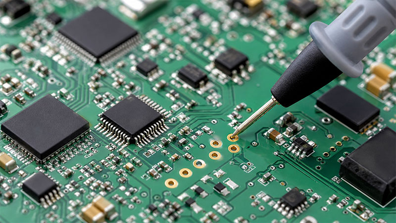
Step 8 — Automated Optical Inspection (AOI)
AOI machines scan every joint and every placed component. They detect missing parts, polarity errors, tombstoning, solder bridges, and insufficient solder. Anything flagged is reviewed before the board continues to testing.
Step 9 — X-Ray Inspection
For BGAs and QFNs, the solder joints are hidden under the component body. AOI cannot see them. X-ray inspection can. This step is essential for high-reliability applications and for any design with area-array packages.
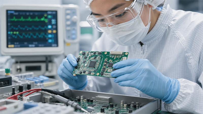
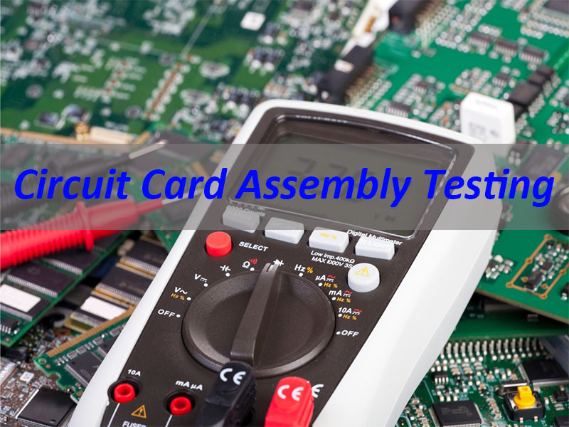
Step 10 — Functional Testing
Finally, each board is powered on and tested against your specification. Depending on volume and requirements, this may use flying probe testing, ICT, or a custom functional test fixture. Only boards that pass leave the facility.
Materials and Surface Finishes for Circuit Board Assembly
The substrate and surface finish you specify affect soldering quality, thermal performance, and shelf life. Here is a practical reference for making those choices.
Substrate Options
| Material | Tg (°C) | Best For |
|---|---|---|
| FR4 Standard (KB 6160, S1141) | 130–140 | General commercial electronics |
| FR4 Mid-Tg (IT 158, S1000H, S1150G) | 150 | Industrial, higher-temperature environments |
| FR4 High-Tg (IT180A, S1000-2M, FR408) | 170–180 | Automotive, power electronics, lead-free assembly |
| High-Speed (M4/M6/M7, TU-872SLK, IT-958) | — | 5G, RF, high-frequency signal integrity |
| Rogers 4350B / 4003, TMM series | — | Microwave, antenna, radar |
| PTFE (Rogers, Taconic, Arlon, Nelco) | — | Ultra-high frequency, aerospace RF |
Surface Finish Options
| Finish | Shelf Life | Key Strength | Common Use |
|---|---|---|---|
| HASL Lead-Free | 12 months | Low cost, robust solderability | General PCBs, through-hole designs |
| ENIG | 12 months | Flat surface, excellent for BGA and fine-pitch | High-density SMT assemblies |
| OSP | 6 months | Flat, RoHS-compliant, lowest cost | High-volume SMT production |
| Immersion Silver | 6 months | Excellent solderability, flat surface | Fine-pitch, RF boards |
| ENEPIG | 12 months | Wire bonding and soldering compatible | Mixed technology, advanced packaging |
| Hard Gold / Soft Gold | 24 months | Contact wear resistance | Edge connectors, gold fingers |
Tip for prototype builds: If your design includes BGA components, ENIG is the safest choice. It gives you a flat, consistent surface that reduces the risk of wetting failures — which are time-consuming to diagnose during early development.
PCB Manufacturing Capability Reference
Knowing your manufacturer’s process window in advance prevents redesigns. The table below reflects EBest Circuit’s verified production parameters, drawn directly from our current process capability document.
| Parameter | Standard | Advanced |
|---|---|---|
| Layer Count | 1–50 layers | Up to 100L (≥50L requires review) |
| Board Thickness | 0.4 – 6 mm | 0.15 – 10 mm |
| Min. Laser Drill | 0.10 mm | 0.070 mm |
| Min. Mechanical Drill | 0.15 mm | — |
| Inner Layer Copper | 0.5 – 6 oz | Up to 20 oz (≥12 oz requires review) |
| Outer Layer Copper | 0.5 – 10 oz | Up to 28 oz |
| Min. Line Width/Space — 1 oz inner | 4 / 4.5 mil | 3.5 / 3.5 mil |
| Min. Line Width/Space — 1 oz outer | 3.5 / 4 mil | 3 / 3 mil |
| Min. BGA Pad Diameter | 10 mil (ENIG: 8 mil) | 8 mil |
| Max. Board Size (≥3 layers) | 580 × 762 mm | 580 × 1220 mm |
| Hole Position Tolerance | ±0.076 mm | ±0.05 mm |
| PTH Aspect Ratio | 12:1 | 25:1 |
For high-frequency designs, EBest Circuit supports Rogers 4350B, Rogers 4003, TMM series, and PTFE-based laminates from Rogers, Taconic, Arlon, and Nelco. Controlled impedance is available with ±10% standard tolerance.
DFM: The Step That Saves the Most Time When Assembling Circuit Boards
Design for Manufacturing (DFM) analysis happens before production starts. Yet it is the step that has the biggest impact on how smoothly the entire assembly process goes.
Here is why. An issue caught at the DFM stage takes a few hours to resolve. The same issue caught after boards have been assembled — or worse, after they have shipped — can require a full respin and weeks of lost time. So while DFM may feel like a delay at the start of a project, it almost always saves time overall.
What a Good DFM Report Covers
- Pad geometry vs. component footprint — mismatches cause tombstoning and cold joints during reflow
- Component clearance from board edge — too little clearance causes damage during depaneling
- Thermal relief on through-hole pads — without it, heavy copper planes prevent proper wave-solder wetting
- Via-in-pad under BGAs — unfilled vias wick solder away and create open joints
- Component orientation consistency — aligning all polarized parts in the same direction reduces placement errors
- BOM consolidation opportunities — reducing unique part count lowers cost and procurement risk
- Stencil aperture sizing — correct aspect ratios ensure proper paste release on fine-pitch pads
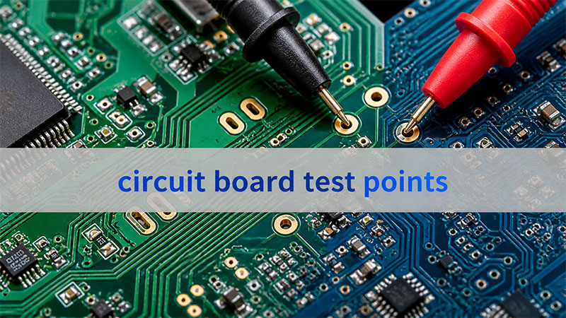
- Test point placement — accessible nodes allow flying probe or ICT coverage without special fixturing
How EBest Circuit approaches DFM: Every order includes a formal DFM pre-review report before production begins. Our engineers have 20+ years of PCB and PCBA experience. In addition to the DFM report, we also provide a BOM optimization list — so component cost and availability issues are addressed before any parts are committed.
Printed Circuit Board Assembly Testing Methods
Testing is the final quality gate. The right method depends on your board complexity, order volume, and the reliability level your application requires. In general, more testing costs more per board — but it costs far less than a field failure.
| Method | What It Detects | Best For |
|---|---|---|
| AOI | Missing parts, polarity errors, solder bridges, insufficient solder | All assemblies — inline after reflow |
| X-Ray | Hidden joint quality — BGAs, QFNs, buried vias | High-density and BGA-heavy boards |
| ICT (In-Circuit Test) | Component values, opens, shorts, basic node function | High-volume production with test fixtures |
| Flying Probe | Opens, shorts, passive values — no fixture needed | Prototypes and small batches |
| Functional Test (FCT) | Full board performance against customer spec | End-product verification at all volumes |
| Burn-In | Early-life failures and infant mortality | Medical, aerospace, defense applications |
As a general rule, flying probe combined with functional testing covers most prototype needs without requiring any fixture investment. For volume production, ICT provides higher throughput and lower per-unit cost once the fixture is paid for.
Prototype and Low Volume Circuit Board Assembly
Not every project starts at high volume. In fact, most engineering projects go through several stages before production ramps up — concept verification, design validation, pre-production pilots, and then volume runs. Each stage has different requirements.
For prototype circuit board assembly, speed and flexibility matter more than unit cost. You want to iterate quickly. You also want to catch design issues before they are locked into production tooling. A good assembly partner at this stage provides active DFM feedback, not just a file-and-run service.
For low volume circuit board assembly — typically defined as batches from 10 to a few hundred units — the priorities shift slightly. Lead time and consistent quality become more important. Component availability also matters more, because spot-buying small quantities introduces substitution risk that a volume buyer can usually avoid.
There is also a practical reason to use the same manufacturer for both prototype and volume work. When you switch suppliers between stages, the process conditions change — solder paste type, reflow profile, stencil design, inspection thresholds. A board validated on one manufacturer’s process may behave differently on another’s. Continuity removes that variable.
At EBest Circuit: We actively support prototype and small-batch orders. Engineers at the R&D and validation stage are a core part of our customer base — not a lower-priority order type. Our 1.5-week PCBA turnaround applies to prototypes as well as volume runs.
How to Choose Circuit Board Assembly Services?
With many suppliers offering circuit board assembly services, it is easy to focus on price and miss the factors that actually determine whether your project succeeds. Here is what to evaluate before committing to a manufacturer.
Match Technical Capability to Your Design
First, check whether the manufacturer can actually build your board. Get their process capability table and compare it to your design parameters — minimum line width, drill sizes, layer count, impedance requirements, and any specialty materials. A supplier who cannot hit your specs is not an option, regardless of price.
Look at Quality Certifications
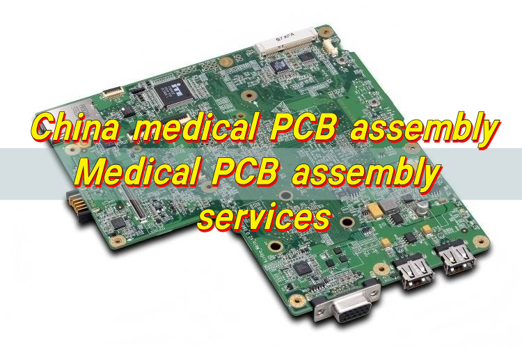
Certifications indicate what kind of manufacturing discipline a company operates under. ISO 9001 is the baseline for general quality management. Beyond that, ISO 13485 covers medical devices, IATF 16949 covers automotive, and AS9100D covers aerospace. These require documented processes, traceability systems, and regular third-party audits — which is exactly what you want in a supplier.
Evaluate Engineering Support
There is a significant difference between a manufacturer who reviews your files before production and one who simply runs whatever you submit. For engineers developing new products, active DFM feedback, BOM optimization input, and process adaptation guidance are worth far more than a marginally lower board price. Problems found before production cost hours. The same problems found after assembly cost weeks.
Ask About Component Sourcing
Counterfeit components are a genuine risk. Ask directly: where do parts come from? Are they sourced from authorized distributors? What does incoming inspection involve? A supplier who cannot answer these questions clearly is a supplier whose component quality you cannot verify.
Check Traceability Systems
For regulated industries — and for any complex product where field failures are serious — traceability matters. Can the manufacturer tell you, after shipment, which component batch was used on a specific board? If they rely on paper records or manual logs, that question may take days to answer. If they use a digital MES, it should take seconds.
Why Engineers Choose EBest Circuit?
EBest Circuit (Best Technology) has specialized in PCB and PCBA manufacturing for over 20 years. In that time, we have served more than 10,000 engineers and 1,800+ customers across industrial, medical, automotive, consumer, and aerospace applications. Here is what makes our approach different in practice.
One Account Manager + Three Engineers per Order
Every project is assigned a dedicated account manager and a three-person engineering team covering process, quality, and DFM. When you have a technical question, you get a response from an engineer with relevant experience. You do not get passed to a general support queue.
DFM Report + BOM Optimization List — Included with Every Order
Before production starts, we deliver a written DFM report with specific, actionable findings. We also provide a BOM optimization list that identifies consolidation opportunities and flags components with availability risk. This service is included as standard, not sold separately.
One-Stop: PCB + Components + PCBA
We operate our own PCB factory and our own PCBA factory. In addition, we work with 1,000+ supply chain partners for component sourcing. As a result, you submit one set of files and receive tested, functional boards — without coordinating between separate fabrication and assembly vendors.
1.5-Week PCBA Turnaround
From Gerber files to shipped, tested boards: as fast as 1.5 weeks. That covers the full cycle — PCB fabrication, component procurement, SMT assembly, inspection, and functional testing. This turnaround applies to prototype orders as well as volume runs.
Full Certification Stack
We hold ISO 9001, ISO 13485, IATF 16949, and AS9100D. This means we are qualified to manufacture for medical, automotive, and aerospace applications — with the documentation and traceability those industries require.
5-Second Material and Batch Traceability
Our digital manufacturing system tracks every component lot and every production batch in real time. Any board can be traced from incoming inspection to shipment — and that trace is retrievable in under five seconds.
To get a quote or discuss your project, contact our engineering team at sales@bestpcbs.com. Send your Gerber files and BOM. We will return a DFM report and a quote within 24 hours.
FAQs About Assembling Circuit Boards
What is printed circuit board assembly?
Printed circuit board assembly (PCBA) is the process of soldering electronic components onto a bare PCB to produce a functional electronic board. It includes solder paste printing, SMT pick-and-place, reflow soldering, through-hole assembly, AOI and X-ray inspection, and functional testing. The finished PCBA can be powered on and integrated directly into a product.
What is the difference between PCB and PCBA?
A PCB is the bare substrate — copper traces, vias, pads, and solder mask, but no components. A PCBA has all components soldered on and has passed inspection and testing. In short, a PCB cannot function on its own. A PCBA can.
How long does circuit board assembly take?
EBest Circuit delivers complete PCBA — covering PCB fabrication, component sourcing, SMT assembly, and functional testing — in as fast as 1.5 weeks. Boards with more complex designs or long-lead components may require additional time. We confirm the expected delivery date at the quoting stage.
What certifications should a PCBA manufacturer have?
ISO 9001 covers general quality management and is the baseline to look for. Beyond that: ISO 13485 for medical devices, IATF 16949 for automotive, and AS9100D for aerospace. EBest Circuit holds all four, which means we can support high-reliability applications across all major industries.
What files do I need for a PCBA quote?
The standard set is: Gerber files, a BOM with manufacturer part numbers and quantities, and a pick-and-place centroid file. An assembly drawing in PDF format is helpful but not always required. Send your files to sales@bestpcbs.com and we will respond with a DFM review and quote within 24 hours.
Do you support SMT and through-hole components on the same board?
Yes. We handle mixed-technology boards with both surface mount and through-hole components. Through-hole soldering is performed by wave soldering or selective soldering, depending on the board layout and proximity to SMT parts.
Can I use the same manufacturer for prototype and volume production?
Yes — and we recommend it. Switching manufacturers between prototype and production changes the process conditions your design was validated against. That is a common and often overlooked cause of unexpected failures. EBest Circuit supports prototype, small batch, and full production from the same facility, so process continuity is maintained from first article through volume shipments.