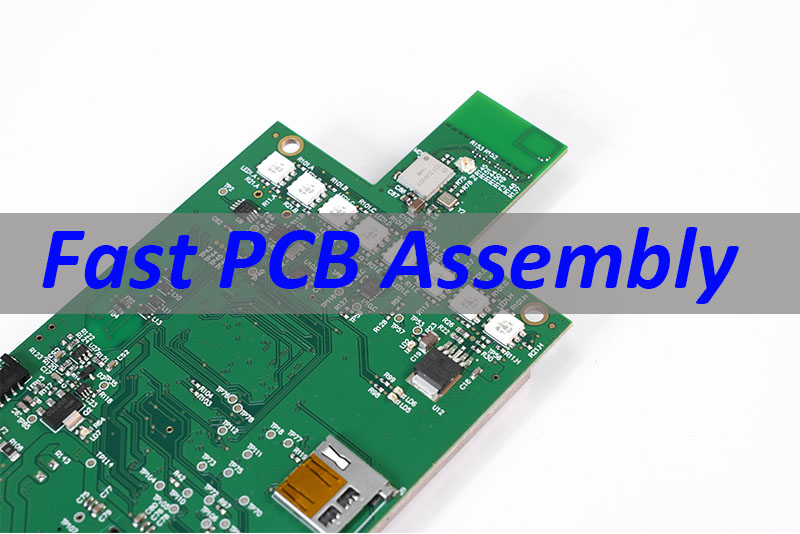
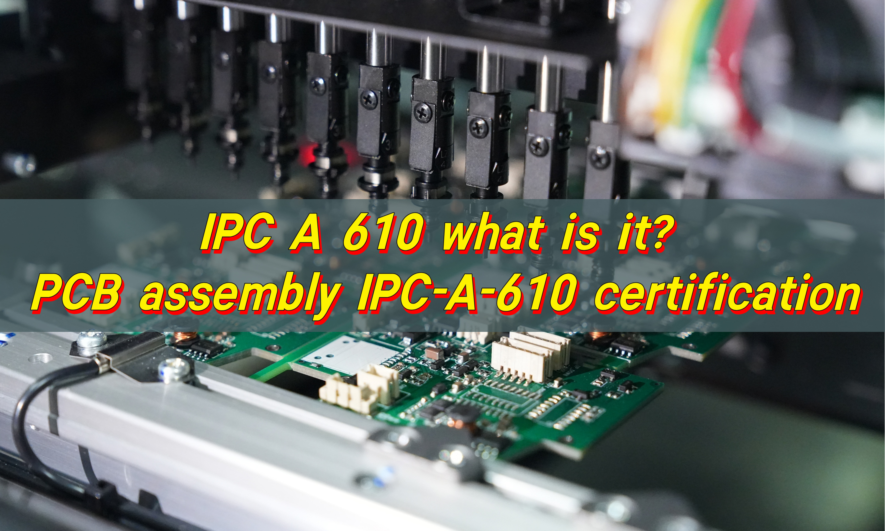
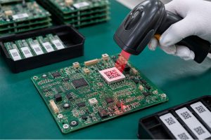
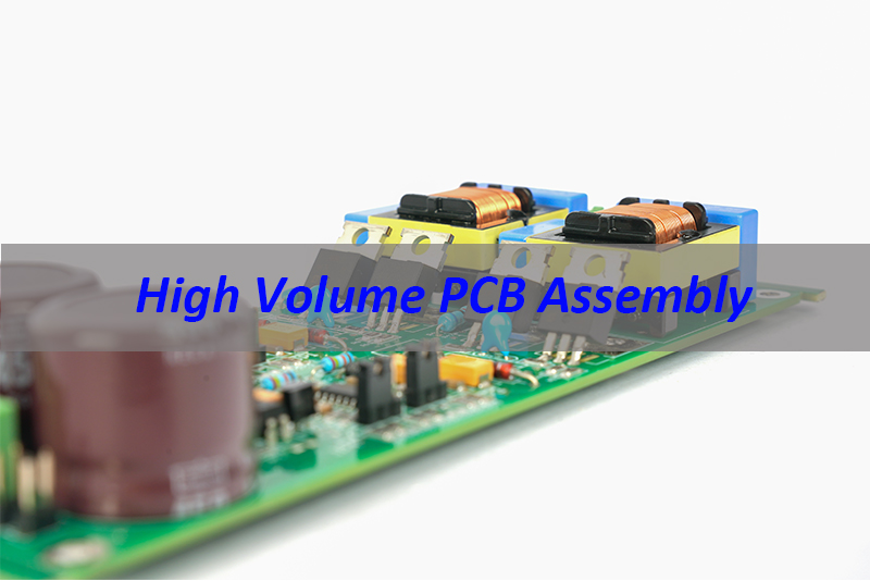
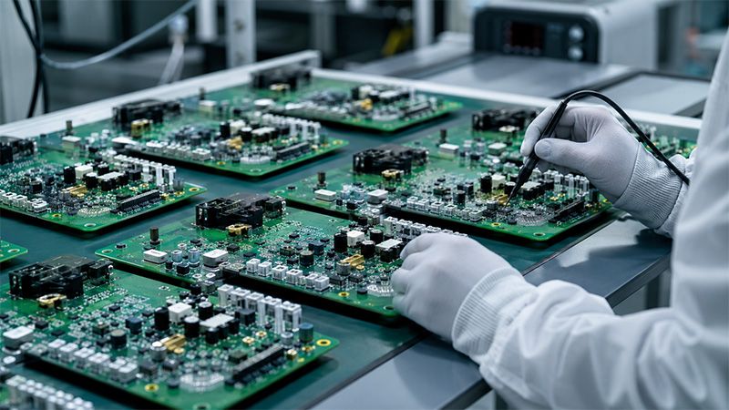
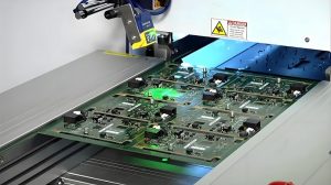
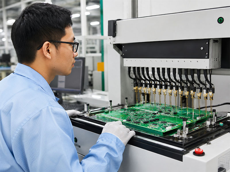
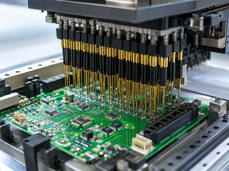
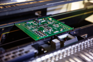
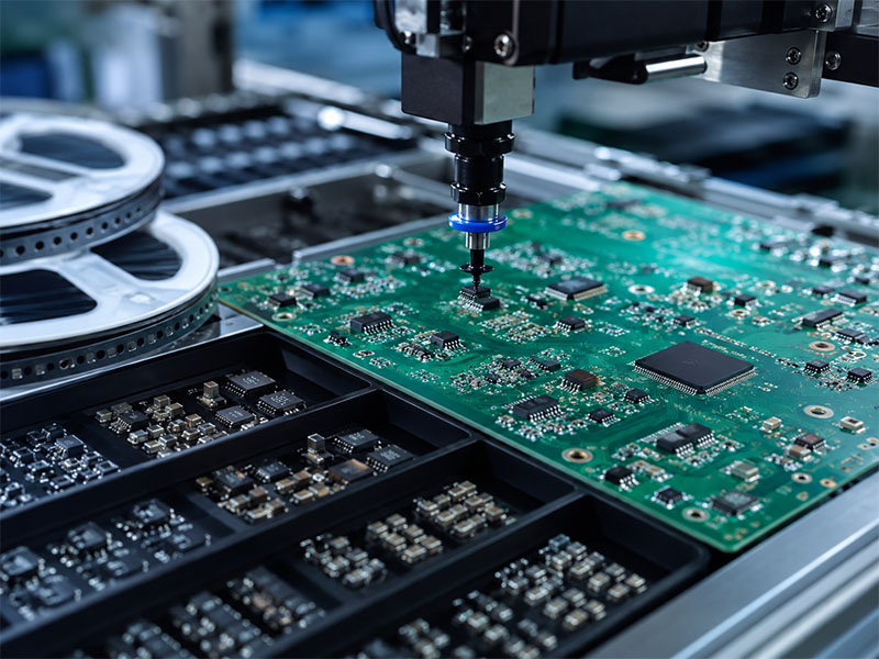
Fast PCB Assembly with Same-Day DFM and BOM Review is the rapid, engineering-validated production service that compresses your time-to-market from weeks to days—without sacrificing quality or compliance. This article explains how EBest Circuit delivers same-day design checks, accelerated fabrication, and full turnkey support for urgent PCBA projects.
The Hidden Risks of Rush Orders
DFM/BOM errors slip through when reviews are rushed or skipped entirely.
Parts shortages stall production after assembly has already started.
Prototype iterations take too long to validate before mass runs.
Turnkey coordination fails between PCB fab, sourcing, and SMT lines.
Quality checks are cut short to meet aggressive lead times.
At EBest Circuit, we solve these issues by embedding engineering validation into every fast-track order—so speed never compromises reliability.
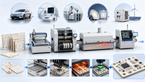
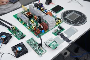
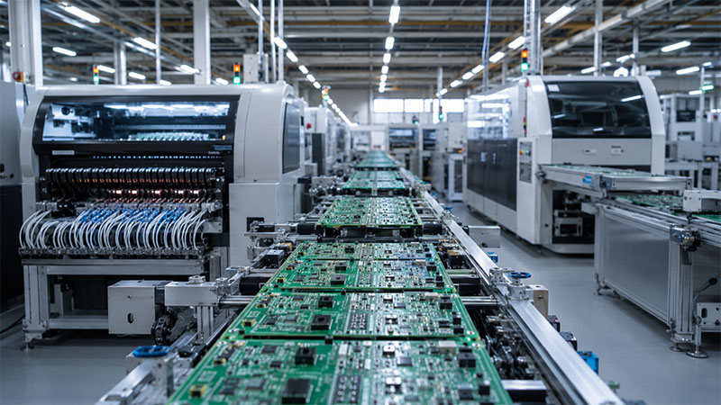
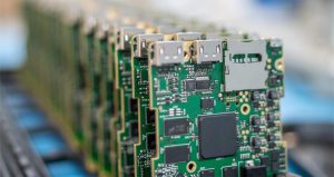
We are a professional fast PCB assembly manufacturer with advanced process capabilities, supporting 1–50 layer boards, HDI, high-frequency materials, and rigid-flex designs. Our integrated workflow covers PCB fabrication, parts sourcing, SMT assembly, and testing—all under one roof. Need a quote or urgent support? Pls feel free to contact us anytime at sales@bestpcbs.com.
Fast PCB Assembly Lead Time Options at EBest Circuit
We offer tiered lead times to match your project urgency, all backed by same-day DFM/BOM validation.
Service Tier
Lead Time
Best For
Ultra-Rush
24 hrs
Prototypes, critical fixes
Priority
48–72 hrs
Small batches, pilot runs
Standard Fast
5–7 days
Low-volume production
All options include free same-day DFM and BOM review—no extra fees, no hidden delays.
Same-Day DFM and BOM Check for Rush PCBA Orders
Our engineering team validates your files within hours of upload, catching issues before they hit the production floor.
Key checks include:
DFM optimization: Line width/spacing, drill tolerances, stack-up alignment.
BOM accuracy: Part availability, alternate sourcing options, lifecycle status.
All inspections are logged and traceable via your project dashboard.
What to Send for a Fast PCB Assembly Quote
To get a quote in <2 hours, send us:
Gerber files (RS-274-X format)
BOM (Excel/CSV with part numbers, quantities, references)
Assembly drawing (optional but recommended)
Special requirements (e.g., conformal coating, panelization)
FAQs about Fast PCB Assembly
Q: Can I get same-day DFM feedback on weekends?
A: Yes—our engineering team operates 7 days a week for urgent requests.
Q: What’s the maximum board size for ultra-rush orders?
A: Up to 580×762mm (larger sizes require 48-hour lead time).
In conclusion, fast PCB Assembly with Same-Day DFM and BOM Review isn’t just about speed—it’s about delivering production-ready boards the first time, every time. From prototype validation to turnkey low-volume runs, EBest Circuit combines advanced process capabilities, global sourcing, and rigorous quality control to keep your project on schedule. Need to accelerate your next build? Pls feel free to contact our team at any time at sales@bestpcbs.com.
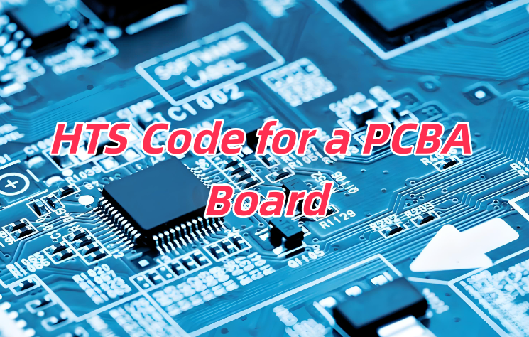
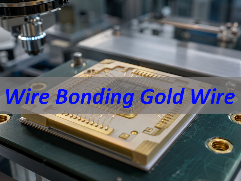
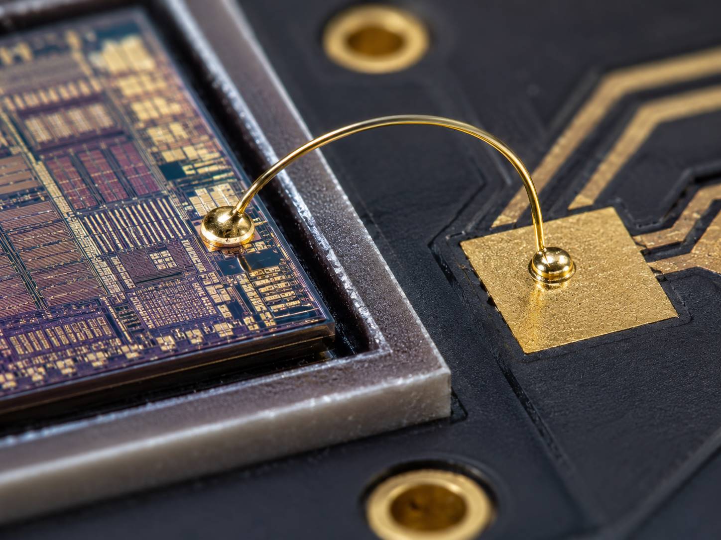
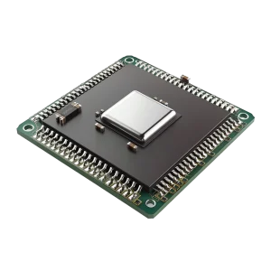
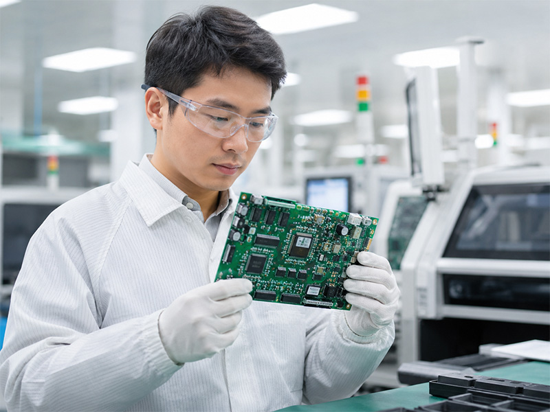
Wire bonding gold wire is a fine gold wire used to connect a chip, die, sensor, module, or substrate pad when standard soldering is not the best connection method. This blog mainly explains how wire bonding gold wire is used in high-reliability PCB and PCBA projects, what process, material, and surface finish requirements should be checked, and how EBest Circuit (Best Technology) supports engineering review, PCB fabrication, PCBA assembly, and testing.
EBest Circuit (Best Technology) supports high-reliability PCB and PCBA projects that involve wire bonding requirements, including PCB fabrication, surface finish review, DFM checking, PCBA assembly, component sourcing, testing, and production traceability. If your project needs a bondable PCB, ceramic substrate, RF module board, sensor board, or high-reliability assembly, you can send Gerber files, BOM, drawings, and requirements to sales@bestpcbs.com for engineering review.
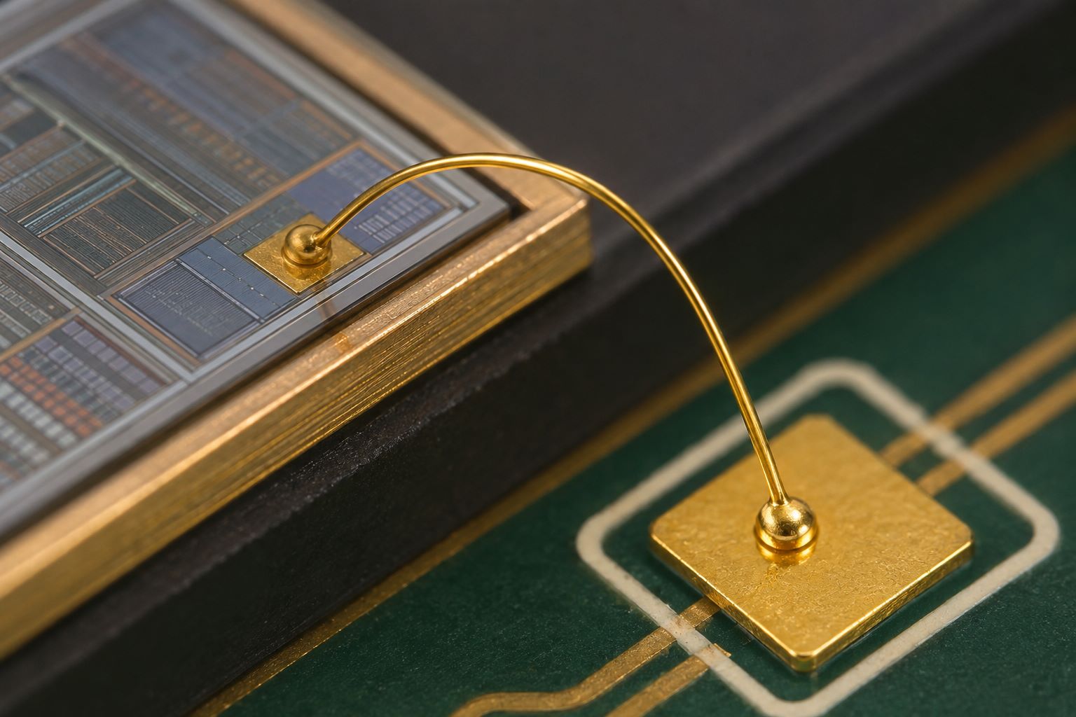
What Is Wire Bonding Gold Wire?
Wire bonding gold wire is a very thin gold wire used to make electrical connections between a small electronic device and a circuit pad. It is common when the design uses bare die, chip-on-board, hybrid circuits, sensors, RF modules, or special high-reliability packages.
In simple words:
It works like a tiny bridge. It connects the chip or die to the PCB, ceramic substrate, package, or module pad.
It is used where soldering is not suitable. Some chips are too small, too delicate, or too specialized for normal SMT soldering.
It needs a bondable surface. The PCB pad cannot be treated like a normal soldering pad only. The surface finish must be suitable for wire bonding.
It is part of the whole PCB/PCBA design. Gold wire bonding is not just a material choice. It affects pad design, surface finish, substrate material, assembly process, and testing.
Common project types include:
Bare die assembly Used when a chip is mounted directly on a board or substrate.
Ceramic substrate modules Used in high-heat, high-power, RF, sensor, and precision circuits.
RF and microwave modules Used where short and stable electrical paths are important.
Medical and industrial electronics Used when reliability, traceability, and long service life matter.
Automotive and aerospace electronics Used in demanding environments where process stability is important.
For customers, the main point is this: if your project needs gold wire bonding, the PCB must be designed and manufactured for it from the beginning.
EBest Circuit (Best Technology) can review bonding pad design, PCB material, surface finish, stack-up, solder mask clearance, and assembly requirements before production. This helps reduce trial-and-error during prototype and batch production.
Why Is Gold Used in Wire Bonding for Electronics and IC Chips?
Gold is used because it is easy to bond, stable, conductive, and resistant to oxidation. For many high-reliability electronics, these properties make gold bonding wire a dependable choice.
Gold is selected for several clear reasons:
Good electrical conductivity Gold helps signals and current pass through fine connections with stable performance.
Strong oxidation resistance Gold does not easily form an oxide layer, so the bonding surface stays more stable.
Good ductility Gold wire can be shaped into loops and bonded without breaking easily.
Mature bonding process Gold ball bonding is widely used and well understood in microelectronics manufacturing.
Reliable long-term performance It is suitable for products that need stable operation over long service life.
Gold wire bonding is often used in:
IC chips
Sensor modules
RF devices
Hybrid circuits
Ceramic substrates
Optoelectronic modules
Medical electronic modules
Automotive sensors
Aerospace electronics
Industrial control modules
For PCB and PCBA buyers, the important question is not only “Why use gold?” The better question is:
Can the PCB pad, surface finish, and assembly process support stable gold wire bonding?
That is where manufacturing support becomes important. EBest Circuit (Best Technology) can help customers check whether the board material, pad finish, and production documents match the bonding requirement before the PCB is fabricated.
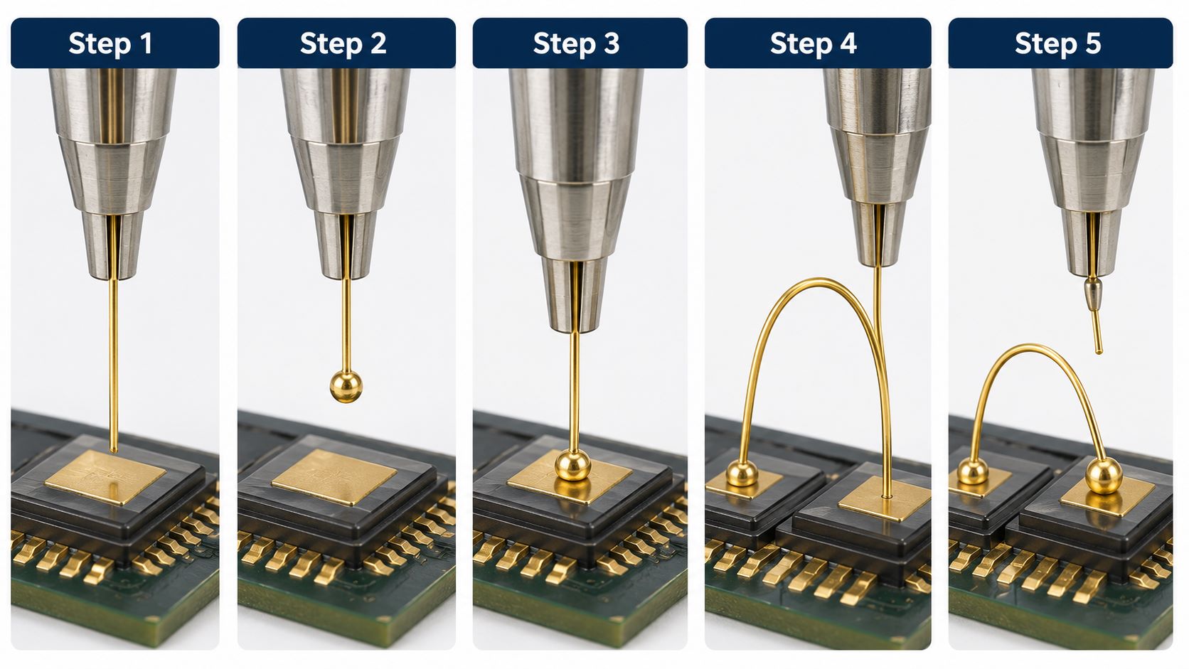
How Does the Gold Wire Bonding Process Work?
Gold wire bonding connects one pad to another using heat, pressure, ultrasonic energy, and a fine gold wire. The process sounds complex, but the basic idea is simple: press the gold wire onto a clean metal pad and create a stable metal-to-metal connection.
A typical gold ball wire bonding process works like this:
Step 1: The gold wire is fed through a bonding tool. The tool guides the wire to the correct pad position.
Step 2: A small gold ball is formed. The end of the wire is melted into a tiny ball.
Step 3: The first bond is made. The gold ball is pressed onto the chip pad or substrate pad.
Step 4: The wire loop is formed. The machine moves to the second pad and creates a controlled wire loop.
Step 5: The second bond is made. The wire is bonded to the second pad, then cut.
The quality of this process depends on a few practical factors:
Pad surface must be clean.
Pad finish must be bondable.
Pad size must match the wire and tool.
Substrate must stay stable during bonding.
Wire loop height must have enough clearance.
Bonding parameters must be controlled.
Inspection and testing must confirm bond quality.
For a PCB project, these details should be confirmed before production. If the board is already made with the wrong finish or poor pad design, bonding problems may appear during assembly.
EBest Circuit (Best Technology) supports this stage through DFM review, fabrication drawing review, surface finish checking, PCB manufacturing, PCBA assembly, and testing coordination. For high-reliability projects, MES traceability can also help track materials, production status, and quality records.
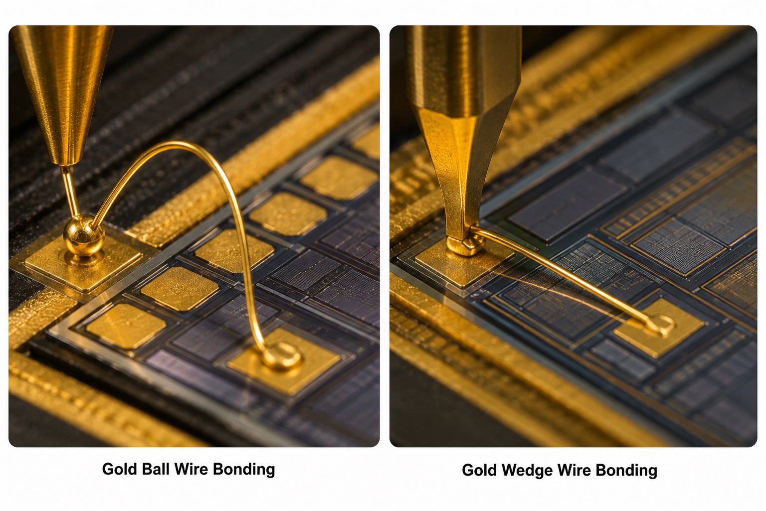
Gold Ball Wire Bonding vs Gold Wedge Wire Bonding: What Is the Difference?
Gold ball wire bonding and gold wedge wire bonding are two common bonding methods. The main difference is the tool shape, bond shape, loop style, and application.
Item
Gold Ball Wire Bonding
Gold Wedge Wire Bonding
Tool
Capillary
Wedge tool
First bond
Ball-shaped
Wedge-shaped
Speed
Usually faster
Usually slower
Direction
More flexible
More directional
Loop profile
Medium or higher loop
Lower loop possible
Common use
IC packaging, chips, sensors
RF, power modules, special layouts
Gold ball wire bonding is common in IC packaging and microelectronics because it is fast, mature, and flexible. It works well when many fine connections are needed.
Gold wedge wire bonding is often used when the design needs a lower wire loop or more controlled wire direction. It can be useful in RF modules, power devices, and compact circuits.
For PCB design, the bonding method affects:
Pad size
Pad spacing
Pad orientation
Wire loop height
Clearance around the bonding area
Surface finish requirement
Inspection method
A simple rule:
Ball bonding is often chosen for speed and flexibility. Wedge bonding is often chosen for low-profile or special layout control.
EBest Circuit (Best Technology) can help customers review the PCB layout based on the expected bonding method. This includes checking pad opening, solder mask clearance, material stability, and whether the board structure is suitable for the assembly process.
What Temperature and Surface Finish Are Needed for Gold Wire Bonding?
Gold wire bonding needs the right temperature and the right pad surface. The exact process window depends on the bonding machine, wire size, pad material, substrate, and reliability requirement.
For customers, the most important point is this:
A normal solderable PCB surface is not always suitable for gold wire bonding.
Surface finish must be selected carefully.
Common surface finishes related to wire bonding include:
Surface Finish
Key Point
Electrolytic soft gold
Common for bondable gold pads
ENEPIG
Often suitable for soldering and wire bonding
ENIG
Must be reviewed carefully
Nickel gold
Can work when thickness and process are controlled
Thick gold plating
Used when stronger bondable gold layer is needed
When choosing the surface finish, check these items:
Gold thickness The gold layer must be suitable for bonding, not only for corrosion protection.
Gold hardness Soft gold is often preferred for bonding because it forms a better bond.
Nickel layer quality Nickel can act as a barrier layer, but poor plating may affect reliability.
Pad cleanliness Contamination can weaken the bond.
Solder mask clearance The bonding tool needs enough open space around the pad.
Storage and packaging Bonding surfaces should be protected from scratches, oxidation, and contamination.
Different PCB materials also behave differently during bonding:
FR4 PCB Suitable for many standard electronic products. For bonding projects, heat resistance and dimensional stability should be checked.
High-Tg FR4 PCB Better for projects with higher thermal stress or stricter assembly requirements.
Ceramic PCB Suitable for high heat, high power, sensor, RF, and precision applications.
Metal core PCB Used for thermal management in LED, power, and high-current products.
RF PCB Used when signal behavior and controlled dielectric performance matter.
Rigid-flex PCB Used when the product needs a compact structure and flexible connection.
How Do Gold, Aluminum, and Copper Wire Bonding Compare?
Gold, aluminum, and copper can all be used for wire bonding. Each material has its place. The right choice depends on the pad material, product requirement, current load, cost target, and reliability level.
Material
Main Strength
Typical Consideration
Gold
Stable and easy to bond
Higher material cost
Aluminum
Cost-effective for many power uses
Oxidation control matters
Copper
Good conductivity and lower cost
Process control is stricter
Gold wire bonding is often selected when reliability, corrosion resistance, and process stability are important.
Best-fit applications include:
IC chips
Sensors
RF modules
Medical electronics
Aerospace electronics
Ceramic substrate modules
High-reliability assemblies
Aluminum wire bonding is common in power devices and some wedge bonding applications.
Best-fit applications include:
Power modules
Automotive power electronics
High-current devices
Some semiconductor packages
Copper wire bonding is used when conductivity and cost control are important, especially in high-volume semiconductor packaging.
Best-fit applications include:
Consumer IC packages
High-volume electronics
Cost-sensitive semiconductor products
The decision should not be based only on wire price. A good material choice should consider:
Bond pad material
Surface finish
Operating temperature
Current requirement
Product life cycle
Vibration or shock
Thermal cycling
Inspection method
Batch quantity
Reliability test standard
For PCB and PCBA projects, the bonding wire must match the board finish and assembly process. EBest Circuit (Best Technology) can support early engineering review so the PCB is manufactured with the correct pad finish, material structure, and process notes.
How to Choose Gold Bonding Wire by Diameter, Resistance, and Cost?
Choosing gold bonding wire is mainly about three things: wire size, electrical performance, and project cost. The goal is not to choose the thinnest or cheapest wire. The goal is to choose a wire that works reliably with the PCB, pad, chip, and assembly process.
When reviewing gold bonding wire, focus on these points:
Wire diameter Thin wire is useful for small pads and fine-pitch designs. Thicker wire can carry more current and provide stronger mechanical performance.
Pad size The pad must be large enough for the selected wire and bonding tool.
Current requirement Higher current may need larger wire, shorter loop length, or better heat dissipation.
Wire length Longer wires may increase resistance and inductance.
Loop height Lower loops help save space. Controlled loop shape is important in RF and compact modules.
Resistance Fine wire still has measurable resistance. This matters in precision circuits and power-related designs.
Inductance In RF designs, bond wire length and loop shape can affect signal performance.
Cost Gold wire cost is influenced by gold price, wire diameter, purity, supplier, and usage volume.
A practical selection path:
Confirm the chip or die pad material.
Confirm the PCB or substrate pad finish.
Define current and signal requirements.
Choose suitable wire diameter.
Check pad size and spacing.
Review loop height and clearance.
Confirm bonding process and inspection method.
Validate with sample production before batch orders.
For buyers, this means one thing:
Do not only ask for a PCB quote. Tell the manufacturer that the board is for gold wire bonding.
This allows the engineering team to check the right details from the beginning.
EBest Circuit (Best Technology) can support customers from prototype to production with:
PCB fabrication
PCBA assembly
DFM review
Surface finish review
Material selection
Component sourcing
AOI, X-ray, electrical testing, and functional testing support
ISO 13485 quality management for medical-related projects
MES-based production traceability
Engineering support for high-reliability applications
This is especially useful for medical, industrial control, automotive electronics, communication equipment, aerospace, RF, sensor, LED, and power electronics projects.
FAQs About Wire Bonding Gold Wire
1. What is wire bonding gold wire used for? It is used to connect chips, dies, sensors, modules, or substrates to circuit pads. It is common in IC packages, ceramic substrates, RF modules, sensor boards, and high-reliability electronic assemblies.
2. Is gold wire bonding the same as soldering? No. Soldering uses solder to attach packaged components to PCB pads. Gold wire bonding uses fine wire to connect a chip or die directly to a pad.
3. Does every PCB support gold wire bonding? No. The PCB must have suitable pad design, surface finish, cleanliness, material stability, and bonding area clearance.
4. What surface finish is usually used for gold wire bonding? Electrolytic soft gold and ENEPIG are commonly considered. ENIG may need special review because standard ENIG is not always suitable for wire bonding.
5. Can FR4 PCB be used for gold wire bonding? Yes, in some projects. The key is to check temperature, flatness, pad finish, and reliability requirements. For higher thermal or precision requirements, ceramic PCB or other special materials may be better.
6. Why is ceramic PCB often mentioned with gold wire bonding? Ceramic PCB has good thermal conductivity, dimensional stability, and high-temperature resistance. That makes it suitable for sensors, power modules, RF devices, LED modules, and hybrid circuits.
7. What is 1 mil gold bond wire? 1 mil gold bond wire has a diameter of about 0.001 inch, or around 25.4 microns. It is a common size in microelectronics, but the final size depends on pad design, current, and reliability needs.
8. Is gold wire better than copper wire? Gold is easier to bond and more resistant to oxidation. Copper has good conductivity and lower material cost, but it needs stricter process control. The better choice depends on the project.
9. What files should I send for a project involving gold wire bonding? Send Gerber files, fabrication drawing, stack-up, BOM, assembly drawing, bonding diagram, pad requirements, surface finish notes, and testing requirements.
10. Can EBest Circuit (Best Technology) support PCB and PCBA projects involving wire bonding requirements? Yes. EBest Circuit (Best Technology) can support PCB fabrication, PCBA assembly, DFM review, material selection, surface finish review, testing coordination, and production traceability for high-reliability PCB and PCBA projects.
11. What board types can EBest Circuit (Best Technology) support? We support FR4 PCB, high-Tg PCB, ceramic PCB, aluminum PCB, copper substrate PCB, RF PCB, rigid-flex PCB, multilayer PCB, heavy copper PCB, and related PCBA assembly projects.
12. How can I get an engineering review? You can send your Gerber files, BOM, drawings, and project requirements to sales@bestpcbs.com. Our team will review the PCB design, material, surface finish, assembly needs, and quotation details.
Need support for a wire bonding-related PCB or PCBA project? Send your files to sales@bestpcbs.com. EBest Circuit (Best Technology) can help review manufacturability, surface finish, assembly process, testing needs, and production feasibility before you move forward.
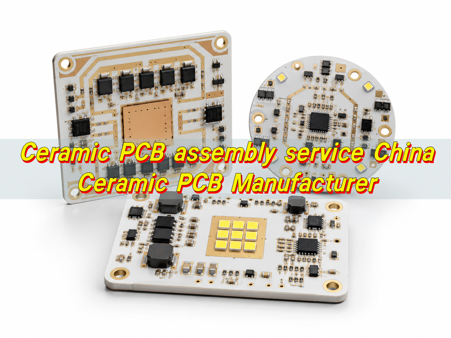
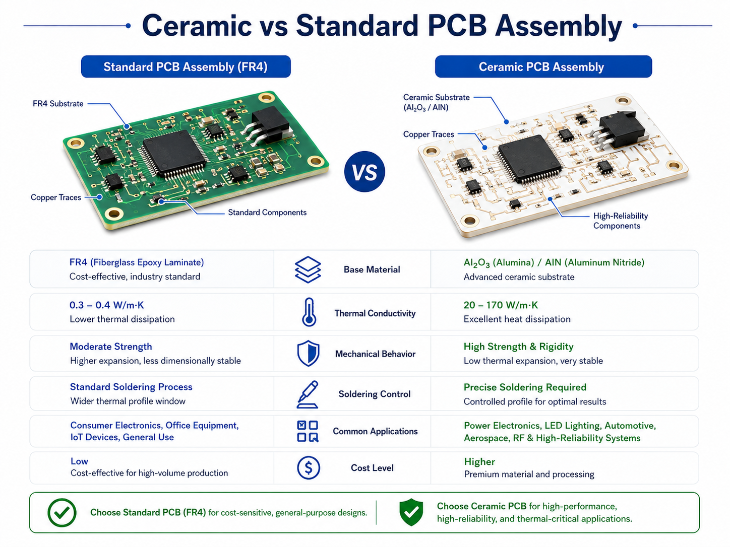
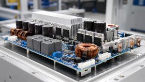
Ceramic PCB assembly is the process of mounting electronic components onto a ceramic PCB board and turning it into a working electronic module. The process may include solder paste printing, SMT placement, reflow soldering, through-hole assembly, inspection, electrical testing, functional testing, and final packaging.
A ceramic PCB is used when a product needs better heat transfer, stable insulation, high dimensional stability, or reliable performance in compact power circuits. These boards are widely used in LED modules, power supplies, automotive electronics, RF products, laser devices, medical equipment, industrial controls, and high-temperature electronics.
Typical FR4 has thermal conductivity of about 0.3 W/m·K. Alumina ceramic is commonly around 24–30 W/m·K, while aluminum nitride can reach about 140–180 W/m·K depending on grade and supplier.
EBest Circuit (Best Technology) supports ceramic PCB fabrication, component sourcing, SMT assembly, through-hole assembly, inspection, and testing. For ceramic projects, the engineering team usually reviews material selection, copper structure, component package, soldering method, and test requirements before production.
How Is Ceramic PCB Assembly Different from Standard PCB Assembly?
Ceramic PCB assembly follows many standard PCBA steps, but the process control is more specific. Standard FR4 boards have moderate flexibility and are easier to handle during panel processing, component insertion, and depaneling. Ceramic boards are dimensionally stable and thermally efficient, but they require more careful handling because the substrate is rigid and brittle.
The copper structure can also be different. Ceramic boards may use DPC, DBC, AMB, thick-film, or thin-film technology. Each process has different copper thickness, line capability, bonding strength, and cost. For example, DBC is often used in power modules because it supports thicker copper and efficient thermal transfer. DPC is often used when fine lines and accurate metallization are required.
The main value of ceramic boards is performance under thermal, electrical, or mechanical demand. The main requirement is disciplined process control. When both are matched, ceramic assemblies can provide stable performance in applications where FR4 may not be suitable.
Can Through-Hole Components Be Used on Ceramic PCBs?
Through-hole components can be used on ceramic PCBs when the hole structure, lead size, soldering method, and mechanical stress are properly reviewed. Although many ceramic pcb boards use SMT components, some products still require pin headers, terminals, connectors, sensors, fuses, or power pins.
Hole formation in ceramic materials is different from FR4 processing. Depending on the material, board thickness, and hole diameter, holes may be made by laser drilling, mechanical drilling, or other ceramic-specific methods. If the hole needs electrical connection, the inner wall must be metallized. Hole tolerance, copper adhesion, and plating quality should be checked before production.
Through-hole assembly is often used in these ceramic PCB applications:
Power modules with high-current pins or screw terminals.
LED driver boards with power input and control connectors.
Sensor modules requiring stable external wiring.
High-voltage boards using leaded components with controlled spacing.
Hybrid assemblies combining SMT parts and through-hole parts.
The soldering method depends on design and volume. Selective soldering, manual soldering, pin-in-paste reflow, or fixture-assisted soldering may be used. The process should control heat input and reduce mechanical force. For heavy components, mechanical support may be needed so the solder joints do not carry the full load during product use.
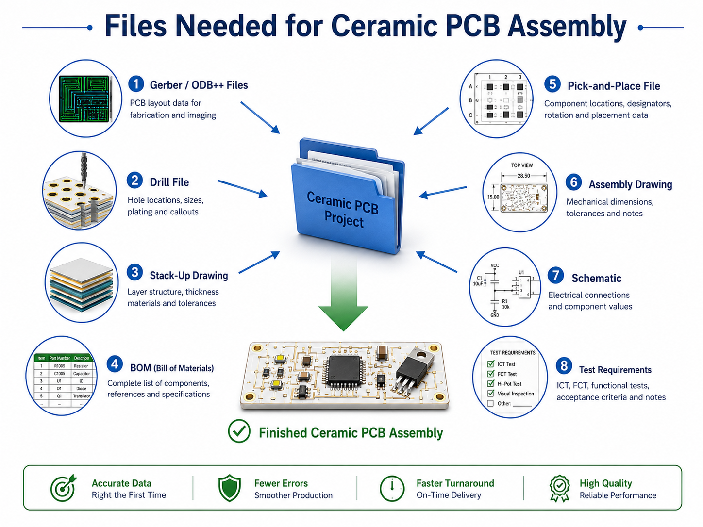
A complete file package helps the manufacturer quote, fabricate, assemble, and test the product correctly. For ceramic PCB assembly, the files should show not only the circuit layout but also the material, copper structure, component position, soldering notes, and test method.
For a ceramic pcb prototype, basic files may be enough for early quotation. For production, the documentation should be more complete, especially for power electronics, medical devices, automotive electronics, aerospace products, and industrial control modules.
A practical file package usually includes:
Gerber files or ODB++ files for PCB fabrication.
Drill files for plated holes, non-plated holes, and slots.
BOM with manufacturer part number, package, quantity, tolerance, and approved alternatives.
Pick-and-place file with coordinates and rotation.
Assembly drawing showing polarity, orientation, special notes, and keep-out areas.
Schematic for engineering review and test planning.
Stencil requirements if solder paste aperture control is already defined.
Test instructions for electrical test, functional test, programming, high-voltage test, or thermal test.
Quality requirements such as IPC class, RoHS/REACH request, inspection criteria, and traceability level.
File Type
Purpose
Why It Matters
Gerber or ODB++
Defines circuit pattern
Confirms pad geometry, copper area, spacing, and fabrication data
Drill file
Defines holes and slots
Supports ceramic drilling and metallization review
Stack-up drawing
Defines material and thickness
Affects heat transfer, insulation, RF behavior, and mechanical strength
BOM
Defines components
Supports sourcing, assembly preparation, and alternative review
Pick-and-place file
Guides SMT placement
Reduces rotation and position errors
Assembly drawing
Shows component orientation and notes
Helps manual inspection and special process control
Schematic
Explains circuit function
Supports DFM review, testing, and troubleshooting
Test document
Defines acceptance method
Confirms how the finished assembly will be verified
For ceramic pcb assembly service China projects, many overseas customers send partial information at the first RFQ stage. That is acceptable for budgetary review. Before production, the manufacturer should confirm all critical data.
EBest Circuit (Best Technology) can review the file package before production and provide feedback on manufacturability, BOM availability, component alternatives, and test planning.
What Should Be Checked Before Ceramic PCB Assembly?
Before assembly starts, the engineering team should confirm whether the design matches the selected ceramic material and production process. Ceramic boards are often used in high-value applications, so early checks can save time during prototype validation and batch production.
The first item is material selection. Alumina is widely used because it offers good insulation, stable performance, and controlled cost. Aluminum nitride is selected when heat dissipation is a major requirement. Silicon nitride is used in some demanding power and automotive applications because it offers good mechanical strength and thermal shock resistance.
The second item is copper structure. Copper thickness, line width, spacing, bonding method, and surface finish must match current load, heat transfer, insulation distance, and soldering requirements. For high-current circuits, thick copper may be required. For fine-pitch circuits, DPC or thin-film ceramic technology may be more suitable.
Pad design should also be reviewed. Large thermal pads can create solder voids if stencil openings are not optimized. Small pads may reduce solder joint strength or thermal transfer. For LEDs, QFN, LGA, MOSFETs, and power ICs, the stencil design, solder paste volume, and thermal pad layout should be checked together.
The BOM should be verified before SMT preparation. The review should cover package type, polarity, MSL level, lead time, lifecycle status, and substitute options.
Key pre-assembly checks include material grade, board thickness, copper thickness, surface finish, pad size, stencil aperture, component orientation, fixture design, handling method, reflow profile, cleaning requirement, test access, and traceability requirement. For high-voltage products, creepage and clearance should be reviewed. For RF products, impedance, dielectric constant, grounding structure, and connector transition should be checked.
EBest Circuit (Best Technology) provides DFM review for ceramic PCB and PCBA projects. The review focuses on practical production points, including material choice, soldering feasibility, component sourcing, inspection access, and testing method.
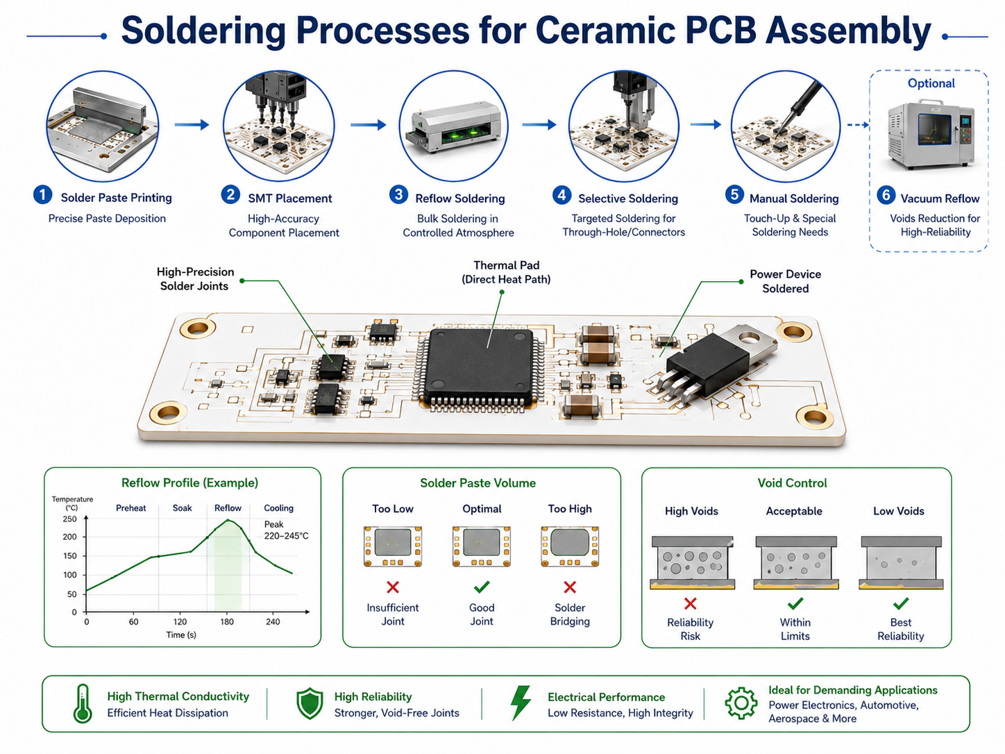
What Soldering Process Is Used for Ceramic PCB Assembly?
The soldering process depends on substrate material, copper structure, component type, board thickness, thermal mass, surface finish, and production volume. Most ceramic PCB assemblies use SMT reflow soldering for surface mount parts. Some products also require selective soldering, manual soldering, pin-in-paste reflow, vacuum reflow, or fixture-assisted soldering.
SMT reflow is used for LEDs, ICs, resistors, capacitors, sensors, RF parts, and many power devices. The process starts with solder paste printing. Components are then placed by SMT equipment, and the board passes through a controlled reflow oven.
Soldering Method
Typical Use
Key Control Point
SMT reflow soldering
LEDs, ICs, resistors, capacitors, sensors, RF parts
Tip temperature, contact time, operator consistency
Pin-in-paste reflow
Through-hole pins assembled during SMT
Paste volume, lead length, hole fill
Vacuum reflow
Power modules and large thermal pads
Void reduction under hidden pads
Fixture-assisted soldering
Special structures or heavy components
Alignment, stability, and heat uniformity
Solder paste selection should match surface finish, component terminal plating, and reliability requirements. Lead-free SAC solder is common, while high-temperature solder or special alloys may be used for certain power or harsh-environment applications. Flux residue requirements should also be confirmed, especially for high-voltage, RF, medical, and clean electronic assemblies.
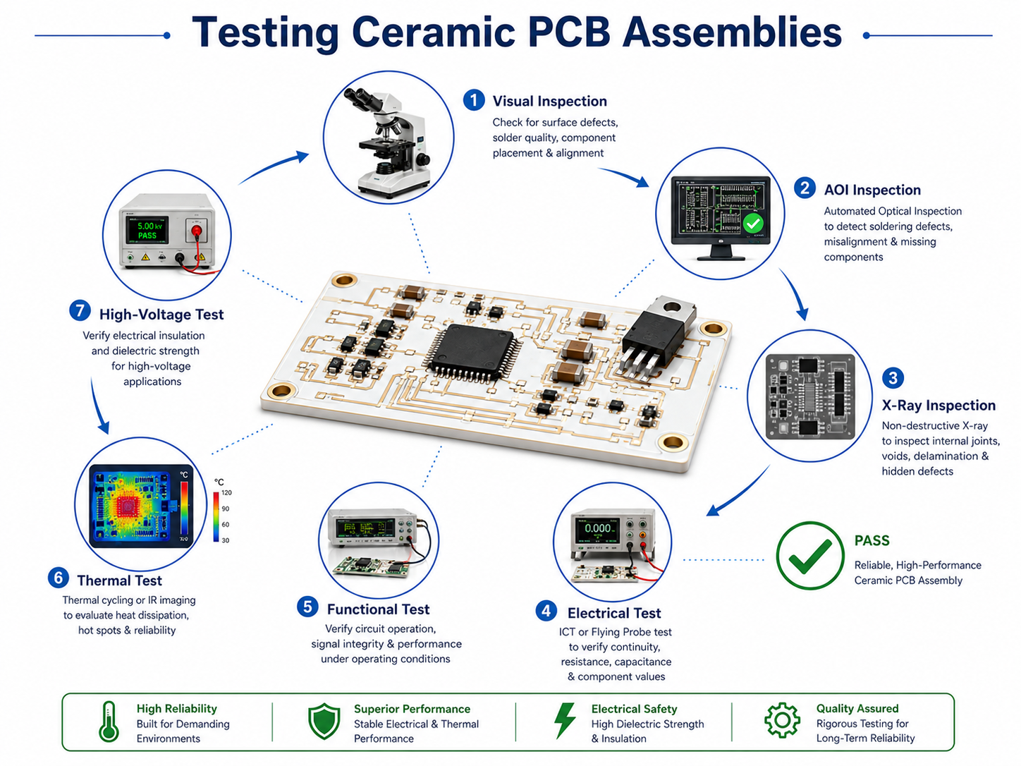
How Are Ceramic PCB Assemblies Tested?
Ceramic PCB assemblies are tested through visual inspection, AOI, X-ray inspection, electrical test, functional test, and application-specific verification. The test plan depends on circuit function, product risk, industry requirement, and customer acceptance criteria.
Visual inspection checks ceramic edges, surface condition, component placement, solder appearance, polarity, marking, contamination, and mechanical damage. Since ceramic substrates are rigid, edge chips and cracks should be checked carefully.
AOI is used after SMT reflow to check missing parts, wrong parts, offset, polarity, tombstoning, solder bridges, and visible solder issues. AOI is efficient for visible components, but it cannot inspect hidden solder joints under BGA, QFN, LGA, or large thermal pads.
X-ray inspection is useful for hidden joints and large thermal pads. It helps identify solder voids, bridging, insufficient solder, and alignment problems.
Electrical testing confirms continuity, isolation, and circuit behavior. Depending on the design, the test may include open/short test, insulation resistance test, high-voltage test, current test, programming, communication check, or full functional test. RF ceramic boards may require impedance-related checks, return loss, insertion loss, or frequency response testing based on product requirements.
EBest Circuit (Best Technology) supports AOI, X-ray, electrical test, functional test, and project-based traceability for ceramic PCB and PCBA projects.
What Common Problems Can Happen During Ceramic PCB Assembly?
Ceramic PCB assembly is reliable when design, material, and process are aligned. Most process issues are linked to material handling, soldering profile, pad design, documentation, or component stress. Early DFM review and controlled production methods can reduce these risks.
Review mounting, insertion force, and reflow profile
Solder voids
Large thermal pads or unsuitable paste/profile
Optimize stencil, paste, reflow, and X-ray control
Poor wetting
Surface contamination or finish mismatch
Control storage and verify solderability
Tombstoning
Pad imbalance or uneven heating
Review pad design, paste volume, and profile
Component shift
Excess paste, vibration, package imbalance
Improve placement and reflow stability
Limited test coverage
Missing test points or unclear procedure
Define test access and acceptance limits early
The practical solution is to review fabrication, assembly, component sourcing, and testing together. A qualified ceramic pcb manufacturer should identify process risks before production and provide clear recommendations for improvement.
What Affects Ceramic PCB Assembly Cost?
Ceramic PCB assembly cost is affected by material, board size, board thickness, copper thickness, metallization method, surface finish, component selection, assembly complexity, test scope, order quantity, and lead time. A ceramic board price is usually higher than FR4 because ceramic materials, fabrication processes, and handling requirements are different.
Material choice is a major factor. Alumina is usually more economical and widely used. Aluminum nitride costs more but provides much higher thermal conductivity. Silicon nitride and other advanced ceramic materials may be selected for mechanical strength, thermal shock resistance, or special operating conditions.
Fabrication method also affects cost. DPC, DBC, AMB, thick-film, and thin-film ceramic processes have different production requirements. Fine lines, tight spacing, thick copper, large copper coverage, and special surface finishes increase process complexity.
Assembly cost depends on component count, package type, placement density, soldering method, and inspection level. Fine-pitch ICs, QFN, BGA, high-power packages, large thermal pads, and through-hole terminals require more process control. X-ray inspection, functional testing, high-voltage testing, thermal testing, programming, conformal coating, and serialization also affect the final cost.
A ceramic pcb prototype usually has a higher unit price because setup, stencil, engineering review, tooling, and process preparation are spread across a small quantity. After the design is verified, batch production can reduce unit cost through better material planning and repeatable process flow.
EBest Circuit (Best Technology) can review stack-up, BOM, assembly method, and test scope during quotation, helping customers understand the main cost drivers before production.
Why Choose China Ceramic PCB Assembly?
China ceramic PCB assembly is widely used by global electronics companies because it combines PCB fabrication, component sourcing, SMT assembly, testing, and production scaling in one mature supply chain.
A capable China ceramic PCB assembly partner can support LED modules, power electronics, industrial controls, RF devices, medical electronics, automotive assemblies, and high-temperature products.
Component sourcing is also important. Many ceramic PCB projects use LEDs, power semiconductors, RF parts, connectors, sensors, passives, and thermal materials. A supplier with sourcing capability can check lead time, lifecycle status, approved alternatives, and package compatibility before assembly.
When choosing ceramic pcb assembly service china, buyers should evaluate capability, not only price. The supplier should understand ceramic materials, copper structure, soldering control, void inspection, through-hole processing, functional testing, and English technical communication.
EBest Circuit (Best Technology) provides ceramic PCB fabrication, component sourcing, SMT assembly, through-hole assembly, testing, and engineering support. For ceramic projects, the team can review material selection, manufacturability, BOM status, soldering method, inspection requirements, and delivery schedule.tion.
If you are looking for a ceramic PCB manufacturer or need support for ceramic PCB assembly in China, send your drawings, BOM, and project requirements to sales@bestpcbs.com for review and quotation.
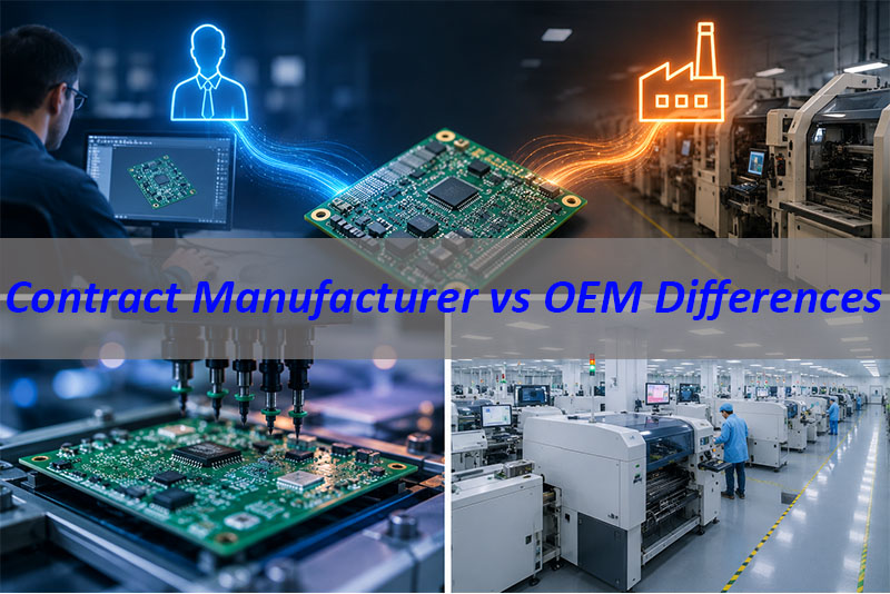
Understanding the contract manufacturer vs OEM differences can save you time, money, and control over your own design. Here’s the twist most guides miss: you are probably the OEM. This article clears up the confusion—and helps you pick the right way to get your product built—in minutes, not weeks.
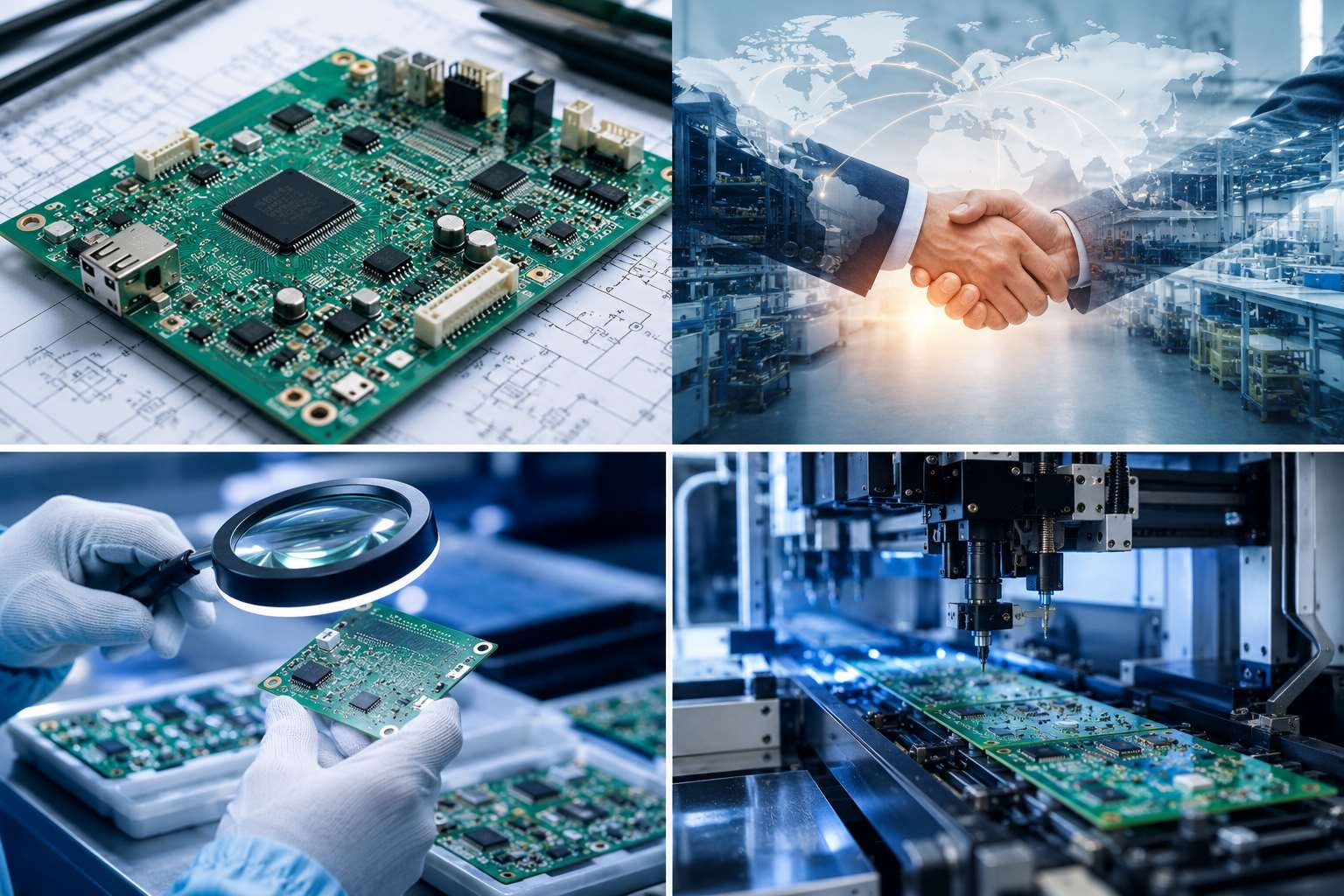
A note on where we fit in: at EBest Circuit (Best Technology), we’re the contract manufacturer—the partner you, as the OEM, can rely on to bring your design to life. With our own PCB and PCBA factories, we’d be glad to take your Gerber files and BOM and handle fabrication, sourcing, assembly, testing, and delivery, while you keep full ownership of your design and IP. If you have a project in mind, we’d be delighted to help—please feel free to reach out at sales@bestpcbs.com for a complimentary DFM review.
What Is an OEM and What Is a Contract Manufacturer?
Here’s the part most articles skip: if you have a product to bring to market, you are the OEM.
OEM (Original Equipment Manufacturer): The brand owner—the company that owns the product, design, and IP and sells it under its own name (Apple, Dell, or your own startup). That’s you.
Contract Manufacturer (CM): The factory you hire to build your product to your design. You send Gerber files + BOM; they fabricate, source, assemble, test, and deliver. You keep the IP.
ODM (Original Design Manufacturer): A factory that hands you a ready-made design to rebrand. You tweak the color or logo; they keep the base design.
So OEM isn’t a supplier you pick—it’s your role. The real decision is how you manufacture: hire a contract manufacturer to build your own design, or take an ODM’s ready design and rebrand it.
What Are the Key Differences Between OEM and Contract Manufacturer?
The honest answer: they aren’t competing options. As the OEM (the brand owner), you hire a contract manufacturer. They’re two sides of the same deal—you own the product; the CM builds it.
The choice that actually matters for you is between your two manufacturing routes:
Contract manufacturer → your design, you own the IP, fully custom.
ODM → their design, you rebrand—faster and cheaper, but you don’t own it.
Ownership drives a lot—but your cost, MOQ, lead time, and customization also depend on tooling, component availability, test requirements, certification needs, and production volume.
Contract Manufacturing vs OEM: A Side-by-Side Comparison
Since you’re the OEM, the comparison that matters is between your two real routes to production: a contract manufacturer vs an ODM.
Factor (you’re the OEM either way)
Contract Manufacturer (build your design)
ODM (rebrand their design)
Who designs it
You
The ODM
Design / IP ownership
Yours
The ODM’s
How much you can customize
Full—built exactly to your spec
Minor (color, logo)
Your upfront cost
NRE, tooling, stencil, fixture, and setup may apply
Lower—the design already exists
Your MOQ
Supplier-dependent; many PCBA CMs support prototype to volume
Often tied to the ODM’s standard MOQ
Your speed to market
Fast once your design, BOM, and tests are finalized
Fastest—the design is ready
Your control
High
Low
Best for you when
You have your own design to protect
You want a fast, low-cost launch
Pros and Cons of OEM vs Contract Manufacturer
You’re the OEM either way—here’s how your two routes stack up:
Contract Manufacturer (build your own design)
For you: Full design & IP control · Fully custom to your spec · Scales with you
Watch out: You need your own design · You’ll rely on a trusted, capable partner
ODM (rebrand a ready design)
For you: Fastest to market · Lower upfront cost · No design work on your side
Watch out: You don’t own the design · Hard to stand out · Others may sell the same base product
When Should You Use a Contract Manufacturer for Your Own Design?
Go the contract manufacturer route—rather than grabbing a ready-made ODM design—when you:
Have your own design or IP to protect
Need custom PCB & PCBA, not an off-the-shelf or rebranded board
Want flexible volumes—samples, small batches, then scale
Need DFM feedback before committing to production
Plan to iterate and own your roadmap
(If you’d rather not own a design and just want a fast, cheap launch, an ODM is the alternative.)
When Does the OEM Model Make Sense?
Being a full OEM—developing and owning your own original product—makes sense when you:
Want long-term brand equity and differentiation
Have the R&D budget and time to develop and maintain a design
Need a proven, fully-owned product line for industries like medical, auto, or aerospace
Want to protect unique IP
In this model you still outsource the actual PCB & PCBA build—usually to a contract manufacturer. The alternative (an ODM) is faster and cheaper, but you give up design ownership.
How to Choose the Right PCB & PCBA Manufacturing Partner
If you own your design, a strong contract manufacturer is usually your best move. Here’s a 6-point checklist for what to look for:
One-stop service — PCB fab + component sourcing + PCBA assembly + testing under one roof, so you don’t juggle vendors.
Real DFM support — A partner who reviews your design before production and flags issues.
Certifications — ISO9001, ISO13485, IATF16949, AS9100D for medical, auto, and aerospace.
Own factory + supply chain — In-house PCB & PCBA plus a deep parts network keeps your quality and lead times under control.
Sample & small-batch friendly — So you can validate before scaling.
Fast, traceable delivery — Quick turnaround with full batch traceability.
Own factories (PCB + PCBA) and 1,000+ supply-chain partners—your quality and lead times are easier to control.
20 years in PCBA, trusted by 10,000+ engineers and 1,800+ customers.
Digital workshop with 5-second traceability on materials, batches, and production progress.
1.5-week fast PCBA delivery.
📩 Get a quote or free DFM review: sales@bestpcbs.com
FAQs: Contract Manufacturer vs OEM Differences Explained
Is an OEM the same as a contract manufacturer? No—and they aren’t even competing options. An OEM is the brand owner (likely you); a contract manufacturer is the factory you hire to build your design. The OEM owns the product; the CM builds it.
What’s the difference between OEM and ODM? As an OEM, you own your product and design. With an ODM, the factory owns the design and you simply rebrand it. So: OEM = your brand and your design; ODM = their design, your label.
Which is cheaper for me—building my own design or using an ODM? An ODM has the lowest upfront engineering effort because the design already exists. Building your own design through a contract manufacturer may add NRE, tooling, stencil, or test-fixture costs, but you keep full IP and customization control.
Can a contract manufacturer help if my design isn’t finished? Yes. A good CM offers DFM analysis and BOM optimization to refine your design before production. EBest does this for free.
Do I lose my IP with a contract manufacturer? Normally, you keep ownership of your existing design, Gerber files, BOM, firmware, and product IP. That said, you should spell out IP protection clearly in your NDA, manufacturing agreement, tooling agreement, and engineering-change process.
What’s the typical lead time for custom PCBA? It varies, but EBest delivers PCBA in as fast as 1.5 weeks.
Still weighing contract manufacturer vs OEM for your next project? We build everything from rigid, flex, and rigid-flex to multilayer, HDI, metal-core, and high-frequency PCBs—plus full PCBA assembly. Tell us what you’re building at sales@bestpcbs.com, and we’ll help you find the right fit, no strings attached.
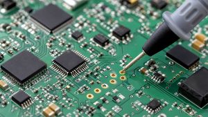
Proto board is often one of the first tools engineers, makers, and product developers use when turning a circuit idea into something they can test on the bench. It gives you a practical way to place components, connect signals, check power paths, and verify whether a circuit behaves as expected before investing in a custom PCB.
For early-stage development, this approach is flexible and cost-friendly. You can adjust wiring, replace components, test different values, and improve the circuit step by step. Once the design becomes stable, the next step is usually a more reliable PCB prototype that can support repeatable testing, better assembly quality, and pilot production.
This guide explains what a proto board is, how it works, how it compares with breadboards and PCB prototypes, how to use and solder it properly, and when it makes sense to move from hand-built wiring to a custom manufactured circuit board.
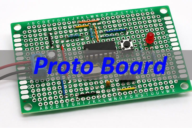
What Is a Proto Board?
A proto board is a board used to build and test electronic circuits before creating a final PCB design. It usually contains a grid of holes, copper pads, or plated-through areas where components can be inserted, soldered, and connected with wires or solder bridges.
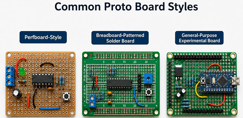
It is also commonly called a prototype board, prototyping board, or protoboard. These terms are often used in similar contexts, although the exact board structure can vary. Some boards are plain perfboards with individual pads, while others follow a breadboard-like pattern that makes circuit transfer easier.
A proto board is useful because it sits between two development stages:
Development Stage
Typical Tool
Main Purpose
Concept testing
Breadboard
Quick, temporary circuit experiments
Functional validation
Proto board
More stable soldered prototype
Product verification
Custom PCB prototype
Repeatable layout, dimensions, and performance
Production
Fabricated PCB / PCBA
Scalable manufacturing and assembly
In simple terms, a proto board helps you move from “the circuit works in theory” to “the circuit works in hardware.”
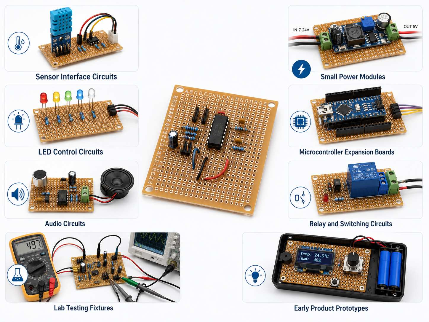
It is widely used for:
Sensor interface circuits
Small power modules
LED control circuits
Microcontroller expansion boards
Audio circuits
Relay and switching circuits
Lab testing fixtures
Early product prototypes
For simple circuits, a proto board can be enough for long-term bench use. For commercial products, however, it is usually a development step before a custom PCB prototype.
When Should You Use One in Electronics Prototyping?
A proto board is most valuable when your circuit has moved beyond a quick breadboard test but is not ready for formal PCB fabrication yet. It gives you more mechanical stability than jumper wires on a breadboard while still allowing design changes.
You can use it when:
The schematic is mostly confirmed
The circuit needs soldered connections for stable testing
The prototype will be handled, moved, or tested repeatedly
The design uses through-hole components
You want to test connector positions before layout design
The circuit is small enough for manual wiring
You are validating a module before creating a full PCB
For example, an engineer may test a temperature sensor circuit on a breadboard first. After confirming the sensor output and microcontroller code, the same circuit can be transferred to a proto board for longer functional testing. This gives stronger connections and fewer loose wire issues.
A proto board is also helpful when evaluating component values. You can test different resistors, capacitors, connectors, or interface parts before locking the design into a PCB layout. That flexibility is one reason it remains popular in engineering labs, schools, repair benches, and product development teams.
For dense circuits, high-speed signals, RF designs, thermal-sensitive power boards, or products that require enclosure fitting, a custom PCB prototype is usually a better next step.
How Does a Proto Board Connect Components?
A proto board connects components through copper pads, plated holes, jumper wires, solder joints, or copper traces depending on the board style.
Most basic boards have individual copper pads around each hole. Components are inserted through the holes and soldered to the pads. The electrical connections are then created manually with:
Solder bridges
Solid-core jumper wires
Insulated hookup wires
Bare copper wires
Pre-designed copper strips
External connectors
Some boards are designed to imitate a breadboard layout. These make it easier to transfer a working breadboard circuit into a soldered format. Other boards are completely open-grid, giving engineers more layout freedom.
A clean build usually starts with the main components first. Connectors, IC sockets, regulators, switches, and larger capacitors are placed before smaller passive parts. After that, power, ground, and signal paths are wired carefully.
The key is to think of the board as a manual circuit layout. Even though it is hand-wired, the same engineering logic still applies:
Keep power paths clear
Keep ground connections short and stable
Avoid crossing too many signal wires
Separate noisy and sensitive areas
Leave room for test points
Mark pin functions and polarity
Inspect each connection before power-on
A proto board may look simple, but poor wiring can affect circuit behavior. A clean layout gives better test results and makes troubleshooting easier.
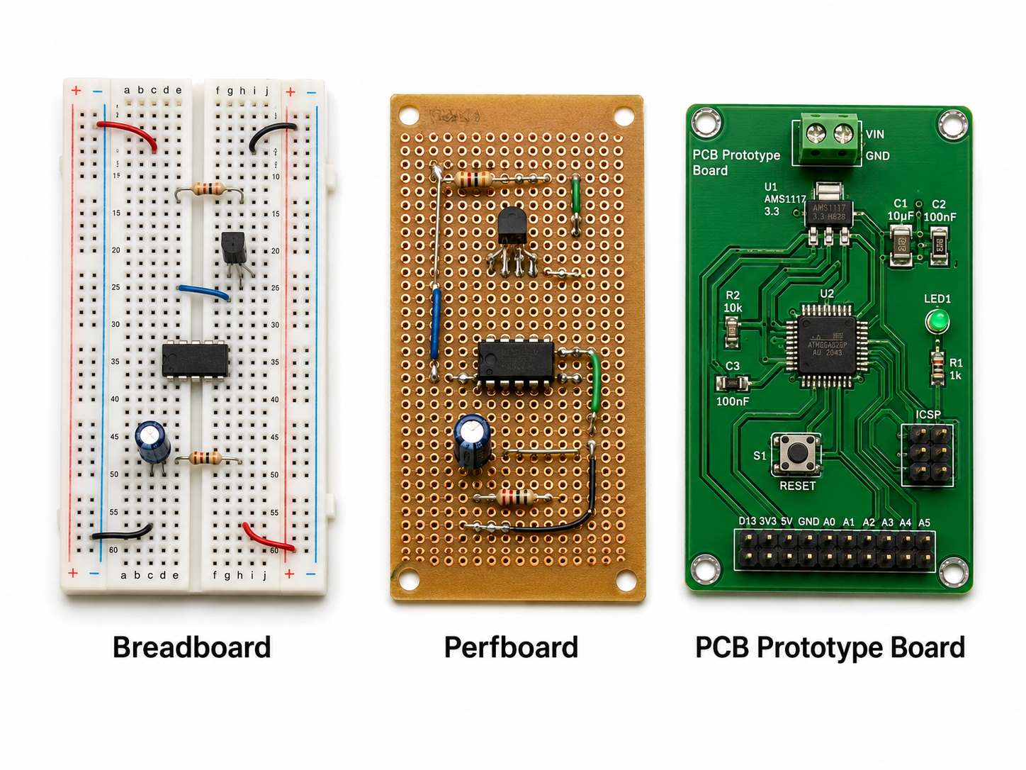
Breadboard, Perfboard, and PCB Prototype Board: What Is the Difference?
Breadboards, perfboards, proto boards, and PCB prototype boards are all used during development, but they serve different purposes. Choosing the right one depends on where you are in the design process.
Board Type
Best For
Connection Method
Reusable
Stability
Breadboard
Fast circuit experiments
Jumper wires and internal clips
Yes
Low to medium
Perfboard
Manual soldered circuits
Point-to-point soldering
Usually no
Medium
Proto board
Stable functional prototypes
Soldering, wiring, or copper pads
Usually no
Medium to high
PCB prototype board
Pre-production validation
Designed copper traces
No
High
A breadboard is best for very early testing. It allows fast changes without soldering. The trade-off is that jumper wires can become loose, contact resistance may vary, and layout control is limited.
A perfboard is a perforated board with holes and copper pads. It gives a permanent soldered structure, but every electrical connection is usually made by hand.
A proto board can refer to several prototype board styles, including perfboard-like designs, breadboard-patterned solder boards, and general-purpose experimental boards. It gives more stability than a breadboard while keeping flexibility.
A PCB prototype board is different because it is designed from CAD files and manufactured with defined copper traces, solder mask, drill holes, surface finish, and controlled dimensions. It is the better option when the design needs repeatability, assembly control, and product-level testing.
For early learning or small experiments, a breadboard or proto board works well. For engineering validation, customer samples, pilot runs, or commercial hardware, a custom PCB prototype gives a more dependable result.
Which Type of Prototype Board Should You Choose?
Different prototype boards are designed for different development tasks. Instead of choosing only by size or price, it is better to choose based on the circuit type, component package, wiring density, and testing goal.
For through-hole circuits, a standard proto board or perfboard is often the easiest choice. It works well for resistors, DIP ICs, headers, switches, connectors, relays, and electrolytic capacitors.
For surface-mount components, an SMD prototype board is more suitable. These boards include pad patterns for common packages such as SOIC, SOT-23, 0805, 0603, QFN adapters, or other small footprints. They are useful when testing modern ICs that are not available in through-hole packages.
For development boards, Arduino or Raspberry Pi expansion boards can speed up testing. They provide compatible header spacing and make it easier to connect sensors, modules, displays, or driver circuits.
For compact circuits, a mini prototype board saves space and works well for small sensor modules, LED circuits, or simple interface boards.
For lab use, a proto board kit can be practical. It often includes different board sizes, headers, jumper wires, terminal blocks, and small accessories for daily testing.
When the circuit becomes complex, manually selecting a larger proto board is not always the best answer. At some point, the project benefits more from a custom PCB layout with fixed routing, correct footprints, mounting holes, and cleaner assembly.
How to Build a Simple Circuit Step by Step
Building a circuit on a proto board is easier when the process is organized. A good workflow prevents messy wiring and reduces debugging time.
1. Review the schematic first
Start with a clear schematic. Confirm component values, pin numbers, power input, ground points, connector orientation, and signal direction before placing anything on the board.
2. Place the main components
Put larger or more important parts first. IC sockets, connectors, switches, regulators, relays, and terminal blocks should be positioned with enough spacing around them.
3. Plan the power and ground paths
Power and ground should be easy to identify. Use thicker wires for higher current paths and avoid routing power through thin, weak connections.
4. Group related components
Place supporting resistors, capacitors, and protection parts close to the IC or connector they support. This makes the circuit easier to read and improves electrical behavior.
5. Add signal connections carefully
Use short and direct wires where possible. For analog or sensitive signals, keep them away from switching nodes, relays, motors, and high-current paths.
6. Solder in stages
Do not solder everything at once. Complete one section, inspect it, then move to the next. This makes mistakes easier to find.
7. Check continuity before applying power
Use a multimeter to confirm power, ground, and important signal paths. Check for shorts between power and ground before turning the circuit on.
8. Power up gradually
If possible, use a current-limited power supply. Start with a low current limit, then verify voltage rails and key signals step by step.
This process turns a hand-built circuit into a more controlled engineering sample. It also creates useful reference information for the later PCB layout stage.
Layout, Wiring, and Soldering Tips for a Cleaner Build
A well-built proto board is easier to test, modify, and convert into a PCB design. The goal is not only to make the circuit work, but to make it understandable.
Keep the layout readable
Place the circuit in a logical direction. For example, power input can start from one side, signal input from another side, and output connectors near the edge. This makes testing and troubleshooting more efficient.
Use short wiring where possible
Long jumper wires add clutter and can pick up noise. Shorter wires make the board stronger and cleaner.
Separate power and signal paths
Power circuits, switching circuits, and motor drivers can introduce noise. Keep sensitive analog lines, sensor signals, and communication traces away from these areas.
Mark important pins
Label voltage input, ground, signal pins, polarity, and connector direction. Even simple labels can prevent mistakes during testing.
Use good soldering practice
A proper solder joint should be smooth, shiny, and mechanically stable. Cold solder joints, excess solder, and weak pad connections can create intermittent faults.
Leave space for test points
Add accessible points for measuring voltage, current, PWM signals, I2C, SPI, UART, reset lines, and sensor outputs. Debugging is much easier when test access is planned.
Inspect before each major test
A visual inspection and continuity test can catch many problems early. Look for solder bridges, reversed components, loose wires, wrong pin connections, and overheated pads.
For simple low-speed circuits, these tips are often enough. For RF circuits, high-speed digital interfaces, precision analog boards, or power electronics, a custom PCB prototype gives better control over impedance, grounding, thermal paths, and repeatability.
When Should a Prototype Become a Custom PCB?
A working hand-wired prototype is an important milestone, but it is usually not the final hardware format. Once the circuit has been verified, a custom PCB makes the design cleaner, stronger, and easier to reproduce.
You should consider moving to a custom PCB when:
The circuit function has been confirmed
Wiring becomes crowded or difficult to trace
The same board must be tested several times
Connector location and board size matter
The product must fit inside an enclosure
The circuit includes high-speed, RF, or noise-sensitive signals
Thermal performance becomes important
The project is moving toward pilot production
Assembly time is becoming too long
The design requires consistent quality across multiple units
A custom PCB prototype allows the copper traces, component footprints, mounting holes, solder mask, silkscreen, and surface finish to be controlled. It also makes PCBA assembly more practical.
This step is especially valuable when a product team wants to reduce hand-wiring errors, improve test consistency, and prepare for customer samples or small-batch production.
Before production, the design should go through proper engineering review. Gerber files, drill files, stackup, copper spacing, solder mask clearance, component footprints, BOM availability, and assembly requirements should all be checked. This is where a professional PCB manufacturer can add real value.
Case Study: 4-Layer FR4 PCB Prototype from a Customer’s Proto Board Project
After testing the circuit on a proto board, the customer wanted a more stable PCB prototype for the next development stage. The hand-wired prototype had already proved the basic function, but it was not suitable for repeat testing, assembly review, or small-batch preparation.
To move the project forward, we manufactured a 4-layer FR4 PCB prototype based on the customer’s confirmed design files.
Customer Requirement
The customer needed a board that could provide:
More reliable electrical connections than hand wiring
A fixed layer structure for engineering validation
Stable board thickness for assembly and enclosure checking
Clear solder mask and silkscreen for component identification
A practical surface finish for prototype testing
Our Manufacturing Support
Before production, our engineering team reviewed the PCB files and confirmed the key manufacturing details, including layer count, material grade, copper thickness, board thickness tolerance, solder mask, silkscreen, and surface finish.
For this project, we used FR4 TG170 material to provide better thermal stability during soldering and assembly. The board was produced with 1 oz copper on all four layers, which offered a balanced structure for prototype-level testing.
The board also used green solder mask, white silkscreen, and lead-free HASL surface finish, making it practical for engineering samples, functional testing, and further design review.
Project Specification
Item
Specification
PCB Type
4-Layer FR4 PCB
Material
FR4 TG170
Copper Thickness
1/1/1/1 oz
Board Thickness
1.6 mm ±10%
Solder Mask
Green
Silkscreen
White
Surface Finish
Lead-Free HASL
Production Stage
PCB Prototype / Engineering Validation
Result
The finished PCB gave the customer a cleaner and more repeatable platform than the original proto board. It helped the project move from early circuit testing to a more controlled PCB prototype stage, ready for assembly review, functional testing, and future small-batch production.
Why Choose Us for PCB Prototype Manufacturing After Proto Board Testing?
After a circuit works on a proto board, the next challenge is turning it into a manufacturable PCB. This step requires more than simply drawing copper traces. A reliable manufacturing partner should help review the design from fabrication, assembly, sourcing, and testing perspectives.
At EBest Circuit, we support customers from early PCB prototype to PCBA assembly and small-batch production. Our team can help convert verified prototype concepts into practical circuit boards with better layout control, cleaner assembly, and stronger production readiness.
Engineering Support Before Production
We can review Gerber files, stackup, copper spacing, drill design, solder mask clearance, impedance requirements, component footprints, and assembly risks before production starts. This helps reduce avoidable issues before boards enter fabrication.
From PCB Prototype to PCBA Assembly
Once your circuit has been tested on a proto board, we can support the next stage with PCB fabrication, component sourcing, SMT assembly, through-hole assembly, inspection, functional testing, and box-build assembly when required.
DFM Review and BOM Optimization
A hand-built circuit may work electrically, but it still requires manufacturability review before it becomes a stable PCB. We can help check layout risks, part availability, alternative components, assembly feasibility, and production consistency.
Our production support can include material control, drilling inspection, solder mask control, surface finish inspection, electrical testing, AOI, X-ray inspection when required, and functional testing for assembled boards.
One-Stop Service for Product Development
For engineering teams, one-stop support reduces communication gaps between PCB fabrication, component sourcing, assembly, and testing. It also helps the project move from bench prototype to repeatable hardware with fewer handoff problems.
If your circuit has already been verified on a proto board, we can help you take the next step. Send your schematic, Gerber files, BOM, or prototype photos to our team for review and quotation.
FAQs About Proto Board
Q1: Is a proto board the same as a breadboard? A1: Not exactly. A breadboard is usually solderless and reusable, while a proto board is commonly used for soldered prototypes. A breadboard is better for quick experiments, and a proto board is better for a more stable circuit build.
Q2: Can you solder components directly on a proto board? A2: Yes. Most proto boards are designed for soldering through-hole components, wires, headers, connectors, and small modules. For surface-mount parts, an SMD-compatible prototype board or adapter board is usually more suitable.
Q3: What is the difference between a proto board and a PCB prototype board? A3: A proto board is usually hand-wired or manually soldered. A PCB prototype board is manufactured from design files with defined copper traces, drilled holes, solder mask, surface finish, and board dimensions. The PCB version is more repeatable and better for product validation.
Q4: Can a proto board be used for SMD components? A4: Yes, but it depends on the board type. Standard through-hole boards are not ideal for small SMD packages. For SMD testing, use a board with matching surface-mount pads or an adapter module.
Q5: How do you test a proto board before powering it on? A5: Start with visual inspection, then use a multimeter to check continuity, power-to-ground shorts, component polarity, and important signal paths. For safer testing, power the circuit with a current-limited supply.
Q6: Is a proto board suitable for high-speed or RF circuits? A6: It can be used for very basic experiments, but high-speed and RF circuits usually require controlled layout, impedance design, grounding strategy, and material selection. A custom PCB prototype is usually better for those applications.
Q7: When should I convert a proto board design into a custom PCB? A7: Convert it when the circuit function is verified, wiring becomes dense, board size matters, testing must be repeatable, or the project is moving toward pilot production. This step helps improve reliability, assembly quality, and product readiness.
Q8: Can you manufacture a PCB prototype based on my proto board circuit? A8: Yes. If you can provide the schematic, connection notes, photos, BOM, or existing layout idea, our engineering team can help review the design and support PCB prototype manufacturing, component sourcing, PCBA assembly, and testing.
In conclusion, a proto board is a practical bridge between circuit ideas and real hardware. It helps engineers test connections, adjust components, verify functions, and understand how a circuit behaves before investing in a custom PCB. For early development, it offers flexibility. For product validation, a manufactured PCB prototype offers repeatability, cleaner assembly, and better production control.
If your circuit has already worked on a proto board and you are ready to move toward a custom PCB prototype, EBest Circuit can support the next step with PCB fabrication, DFM review, component sourcing, PCBA assembly, testing, and production-quality support. Send us your files or project details at sales@bestpcbs.com to start your PCB prototype quotation.
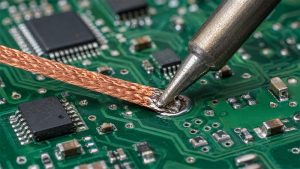
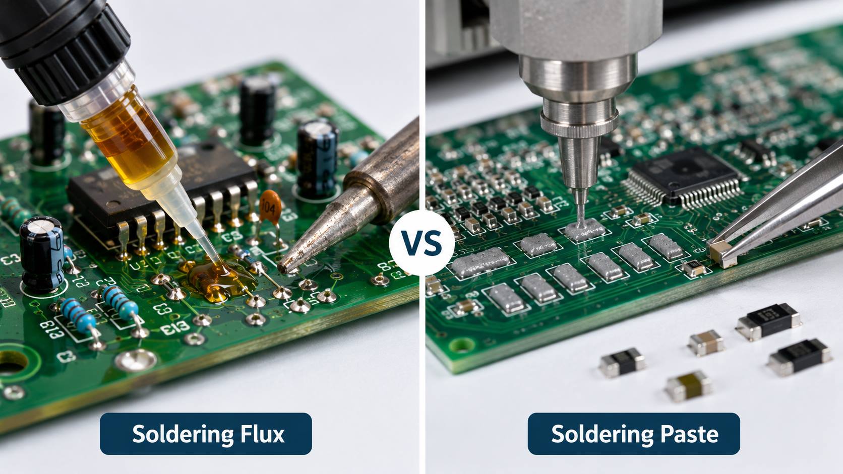
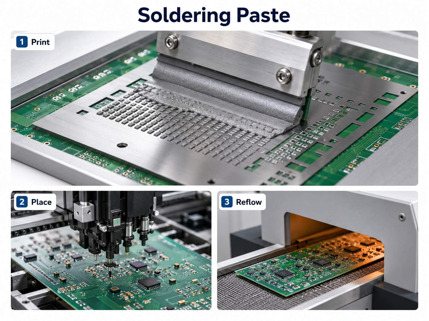
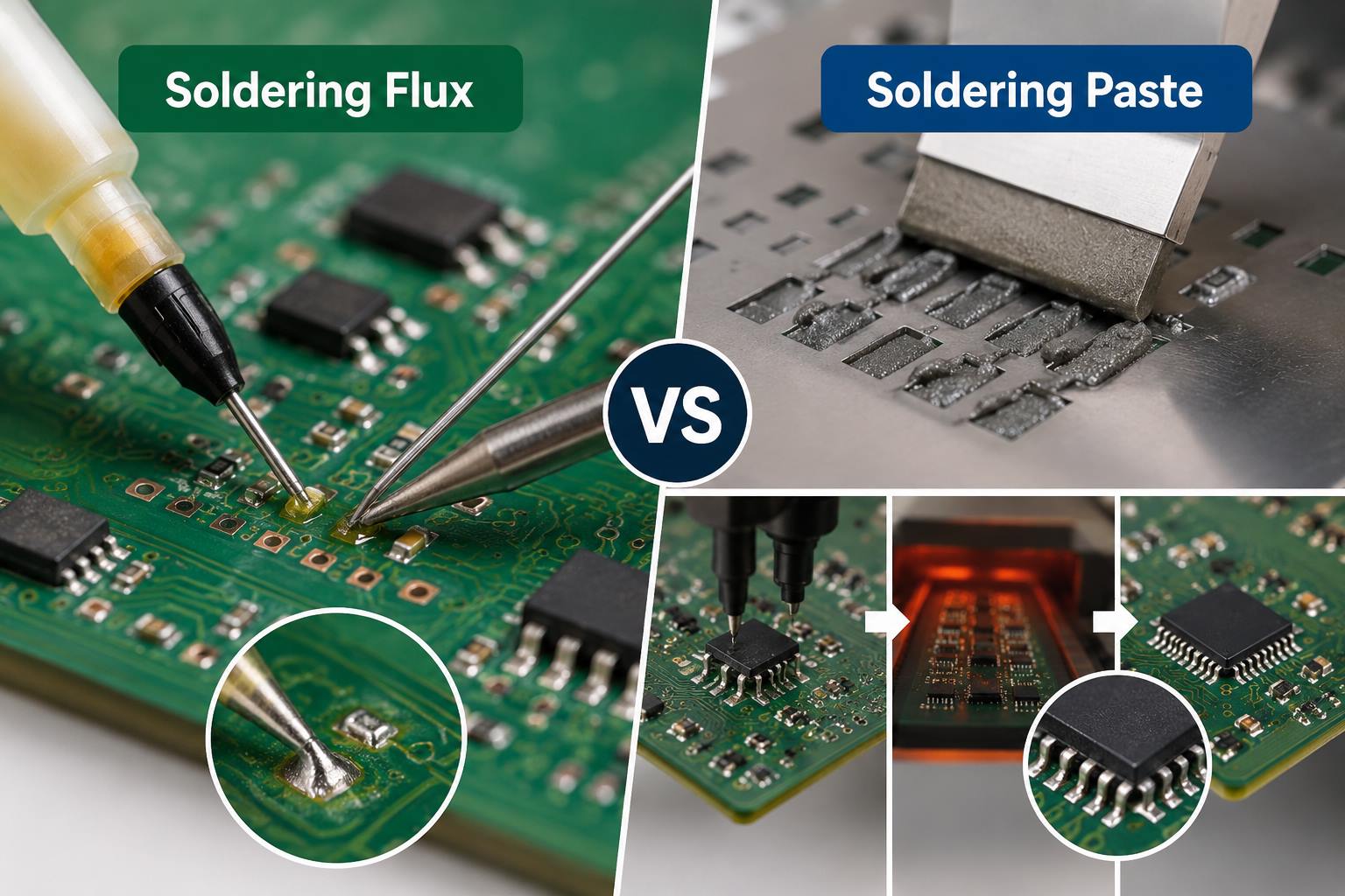
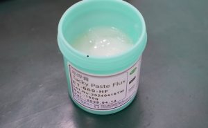
Soldering flux vs soldering paste is a common question in electronics soldering and PCB assembly. The two materials look related, but they do different jobs.
Flux helps solder flow. It removes oxidation and improves wetting.
Soldering paste, also called solder paste, contains solder alloy powder and flux. It can form solder joints during reflow.
So the simple answer is this: flux helps solder work better, while solder paste provides the solder metal and flux together.
This guide explains the difference, when to use each one, and how to avoid common soldering mistakes.
Soldering Flux vs Soldering Paste: Quick Difference
Soldering flux is not solder. Soldering paste contains solder.
That is the biggest difference.
Item
Soldering Flux
Soldering Paste
Main role
Helps solder flow
Forms solder joints
Contains solder metal?
No
Yes
Contains flux?
Yes
Yes
Common form
Liquid, gel, pen, or paste flux
Gray metallic paste
Best use
Hand soldering, repair, rework
SMT assembly and reflow
Application
Brush, pen, syringe, or bottle
Stencil, syringe, or dispenser
Heating result
Cleans and activates the surface
Melts and creates the joint
Think of flux as the helper. Think of solder paste as the joint-forming material.
Flux alone cannot mount an SMT component. It does not supply metal. Solder paste can mount the component because it contains solder alloy powder.
What Is Soldering Flux?
Soldering flux is a chemical material that removes oxidation and helps solder wet metal surfaces.
Copper pads, wires, and component leads can oxidize. Oxidation makes soldering harder. Solder may bead up or refuse to spread.
Flux helps solve this problem.
During heating, flux does three useful things:
Removes light oxidation
Helps molten solder spread
Protects the hot surface from new oxidation
Technicians use flux for hand soldering, PCB repair, wire tinning, connector soldering, and SMT touch-up.
Flux comes in several forms:
Liquid flux
Flux pen
Gel flux
Paste flux
Rosin flux
No-clean flux
Water-soluble flux
For electronics, use electronics-grade flux. Do not use plumbing flux on PCBs. It can damage copper pads and traces.
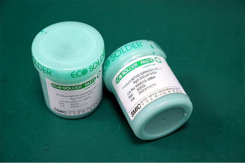
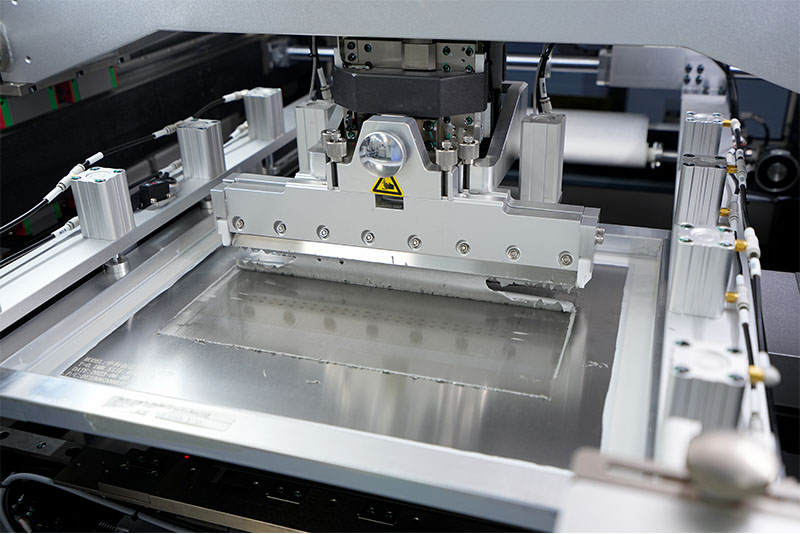
What Is Soldering Paste?
Soldering paste is a gray mixture of fine solder alloy powder and flux. It is mainly used in SMT PCB assembly to form solder joints during reflow soldering.
The alloy powder creates the solder joint. The flux inside the paste helps clean the PCB pads and component terminals during heating.
Pick-and-place machines place components on the paste.
Reflow soldering melts the solder particles.
Cooling forms stable solder joints.
This is why solder paste is widely used for ICs, resistors, capacitors, QFN, BGA, and other surface-mount components.
Common Solder Paste Types We Use
In SMT production, lead-free solder paste is commonly used for RoHS-compliant PCB assembly.
Solder Paste Type
Typical Composition
Common Use
SAC305
Sn96.5%, Ag3.0%, Cu0.5%
Standard lead-free SMT assembly
SAC0307-type
Sn99%, Ag0.3%, Cu0.7%
Lead-free SMT projects with different process needs
Sn63/Pb37
Sn63%, Pb37%
Some special or legacy applications
For most standard SMT projects, we prefer high-temperature lead-free solder paste because it provides better wetting, stronger solder joints, and more stable process control. Medium-temperature solder paste is considered only when heat-sensitive components or special requirements make it necessary.
Solder Paste Handling Control
Good solder paste handling helps reduce printing defects and soldering problems.
Control Item
Our Typical Practice
Storage temperature
2–10°C
Warming time before use
About 4 hours
Mixing time before printing
About 3 minutes
These controls help keep the solder paste viscosity stable before stencil printing.
Why Is SPI Inspection Important?
After solder paste printing, SPI inspection checks whether the paste has been applied correctly.
SPI can inspect:
Paste volume
Paste area
Paste height and thickness
Offset
Bridging risk
Missing paste
Insufficient paste
It helps find common SMT printing issues early, such as missing paste, misalignment, solder bridging, insufficient paste, and paste tailing. Our SPI inspection accuracy can reach around 10 μm, helping improve solder joint consistency before component placement and reflow.
Main Differences at a Glance
Solder paste and flux both support soldering. But they do not replace each other.
Comparison Point
Soldering Flux
Soldering Paste
Composition
Flux chemicals only
Solder powder + flux
Main purpose
Improve solderability
Deposit solder and form joints
Used with
Solder wire, solder bars, existing solder
SMT components and PCB pads
Common process
Manual soldering and repair
Stencil printing and reflow
Storage
Usually room temperature
Often refrigerated
Can form a joint alone?
No
Yes
Common risk
Too much residue
Bridging, solder balls, expired paste
The key point is simple: flux prepares the surface. Solder paste creates the connection.
If you only need better solder flow, use flux.
If you need to place SMT components before reflow, use solder paste.
Is Soldering Paste the Same as Flux?
No. Soldering paste is not the same as flux.
Solder paste contains flux, but flux does not contain solder alloy powder.
This causes confusion because some products use similar names. For example:
Solder paste
Soldering paste
Paste flux
Soldering flux paste
Rosin paste flux
These names may sound similar. But they are not always the same product.
Here is the easy way to check:
Product Name
Usually Means
Solder paste
Solder powder + flux
Paste flux
Thick flux only
Liquid flux
Liquid flux only
Flux pen
Flux in pen form
Rosin flux
Rosin-based flux
If the product does not contain solder alloy powder, it cannot work as solder paste.
Always check the datasheet. Real solder paste usually lists alloy type, metal content, particle size, and reflow profile.
When Should You Use Flux?
Use flux when you already have solder metal.
For example, you may use solder wire with a soldering iron. The wire supplies solder. The flux helps it flow.
Use soldering flux for:
Hand soldering
Wire tinning
Through-hole soldering
Connector soldering
PCB pad touch-up
SMT rework
Component replacement
Oxidized pads or leads
Flux is especially useful when the solder does not wet the pad well. It can also help when you repair an old PCB.
For hand soldering, flux plus solder wire often gives better control than solder paste.
When Should You Use Solder Paste?
Use solder paste when you need to place solder on PCB pads before heating.
This is common in SMT assembly. The paste holds components in place before reflow. Then it melts and forms solder joints.
Solder paste gives better volume control. This matters for small pads and dense PCB layouts.
Too much paste can cause bridging. Too little paste can cause open joints. That is why stencil design, paste quality, and reflow profile matter in PCBA production.
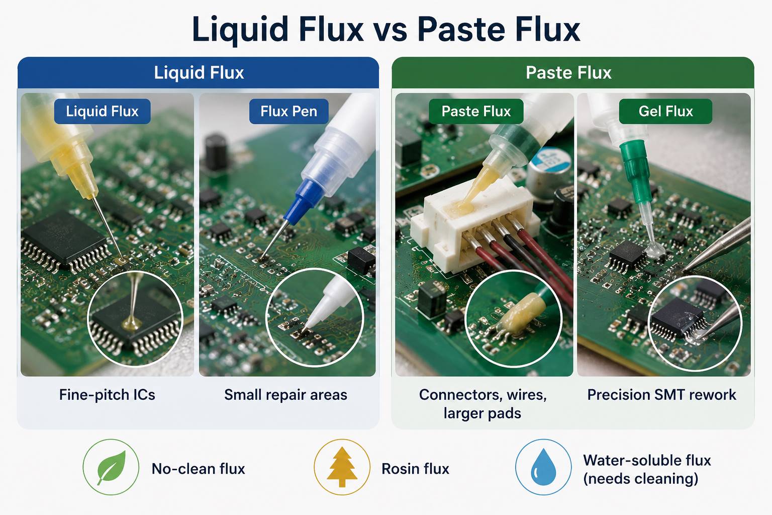
Liquid Flux vs Paste Flux
Liquid flux and paste flux both help soldering. The better choice depends on the job.
Flux Type
Best For
Advantage
Liquid flux
Fine-pitch ICs and PCB touch-up
Spreads quickly
Flux pen
Small repair areas
Easy to control
Paste flux
Connectors, wires, and larger pads
Stays in place
Gel flux
Precision SMT rework
Good placement control
Liquid flux works well for small pads and fine-pitch pins. It flows into tight spaces.
Paste flux works better when you need the flux to stay in one area. It helps with connectors, wires, and larger solder joints.
For electronics, no-clean flux and rosin flux are common choices. Water-soluble flux can also work, but it needs proper cleaning.
Storage and Handling Tips
Solder paste needs stricter control than flux.
Most solder paste should stay refrigerated. Many products require 0–10°C / 32–50°F storage. Before use, let it return to room temperature. This helps avoid moisture condensation.
Do not use expired solder paste for production. Expired paste can dry out, separate, or print poorly.
Flux is usually more stable. Many flux products can stay at room temperature. Still, you should seal the bottle or container after use.
Item
Solder Paste
Flux
Typical storage
Refrigerated
Room temperature
Shelf life
Often 3–6 months
Often 6–24 months
Main risk
Drying, separation, oxidation
Solvent loss, contamination
After opening
Control exposure time
Keep sealed
Expired material
Do not use for production
Not recommended
Good handling helps prevent solder defects. It also improves solder joint consistency.
Common Mistakes to Avoid
Many soldering problems come from simple material mistakes.
Avoid these errors:
Using flux as solder paste
Using plumbing flux on electronics
Applying too much flux
Using expired solder paste
Printing too much solder paste
Heating solder paste with the wrong profile
Forgetting to clean flux when cleaning is required
Using cold solder paste directly from the refrigerator
Also avoid assuming that “no-clean” always means “no concern.” In RF, high-voltage, medical, aerospace, or high-reliability electronics, residue still needs review.
FAQs About Soldering Flux vs Soldering Paste
Q1: Can I use flux instead of solder paste? A1: No. Flux cannot replace solder paste because it does not contain solder metal. It can only help solder flow.
Q2: Does solder paste already contain flux? A2: Yes. Solder paste contains solder alloy powder and flux. The flux helps clean the surface during reflow.
Q3: Do I need extra flux with solder paste? A3: Usually no. Fresh solder paste already contains flux. Extra flux may help during rework, but too much can leave residue.
Q4: Can solder paste be used for hand soldering? A4: Yes, but it is not always the best choice. For normal hand soldering, solder wire plus flux gives better control.
Q5: What happens if I solder without flux? A5: Solder may not flow well. You may see poor wetting, weak joints, solder balls, or dull joints.
Q6: Is paste flux the same as solder paste? A6: No. Paste flux is flux in a thicker form. Solder paste contains solder powder and flux.
Q7: Should flux be cleaned after soldering? A7: It depends on the flux type. Rosin and water-soluble flux often need cleaning. No-clean flux may stay on the board, but sensitive circuits still need review.
Q8: Can I use plumbing flux for PCB soldering? A8: No. Plumbing flux can corrode PCB pads and traces. Use electronics-grade flux only.
To sum up, soldering flux and soldering paste are not the same material.
Flux helps solder flow and wet the surface. Solder paste contains solder metal and flux, so it can form solder joints during reflow.
Use flux for hand soldering, repair, and rework. Use solder paste for SMT assembly, stencil printing, and reflow soldering.
Choosing the right material helps reduce bridging, poor wetting, weak joints, and process waste.
For PCB fabrication and PCBA assembly, EBest supports PCB manufacturing, component sourcing, SMT assembly, soldering process review, testing, and production-quality control. Send your Gerber files, BOM, and assembly requirements to sales@bestpcbs.com for project support.
Billboard defect in SMT is a side-standing chip component defect that happens when a resistor, capacitor, or other small SMD part does not lie flat on the PCB pads after reflow soldering. The part may still touch the pads, but the solder joint is not formed in the correct position. This can raise concerns about electrical contact, mechanical strength, IPC acceptance, and long-term PCBA reliability.
This article explains what billboard defect in SMT means, how it differs from tombstone defect, whether it can be accepted under IPC workmanship standards, why it happens, and how a professional PCBA supplier should inspect and prevent it. The goal is not only to explain the defect, but also to help engineers, buyers, and quality teams judge whether their SMT assembly process is being controlled properly.
EBest Circuit (Best Technology) provides PCB fabrication, component sourcing, SMT assembly, PCBA manufacturing, testing, and box-build assembly support for customers from prototype to mass production. If you are preparing a PCB or PCBA project and want to reduce SMT assembly risks before production, please contact us at sales@bestpcbs.com.
What Is Billboard Defect in SMT?
Billboard defect in SMT happens when a chip component stands on its side instead of lying flat on the PCB pads. The part looks like a small signboard, so this defect is often called billboarding or side stand.
It often appears on small chip resistors and capacitors. It is more common with 0402, 0201, and 01005 parts. These parts are light, small, and easy to move during solder reflow.
A billboarded part may still touch the pads. So, the board may pass a basic electrical test. But this does not mean the solder joint is reliable.
The contact area may be small. The solder joint may be weak. The part may fail later during vibration, heat cycling, handling, or final product use.
That is why a PCBA supplier should not treat billboard defect as a simple visual issue. It needs proper inspection, root cause analysis, and process control.
Billboard Defect vs Tombstone Defect: What Is the Difference?
Billboard defect and tombstone defect are often confused. Both can happen during SMT assembly, but they are different defects.
Item
Billboard Defect
Tombstone Defect
Appearance
Component stands on its side
One end lifts from the pad
Common name
Side stand
Drawbridge
Electrical risk
May still conduct
Often causes an open circuit
Main concern
Weak solder joint
Direct functional failure
Typical judgment
Needs further review
Usually more serious
A tombstone defect usually means one end of the component has lifted away from the pad. This often creates an open circuit.
A billboard defect may still have contact with the pads. However, the solder joint is not formed as designed. The board may work during testing, but the joint may not survive long-term use.
This difference matters. A supplier should not mix these two defects in a quality report. The wrong defect name can lead to the wrong corrective action.
Is Billboard Defect in SMT Acceptable Under IPC Standards?
IPC-A-610 is widely used to judge PCBA workmanship. It helps define what is acceptable, what is a process indicator, and what is a defect.
However, billboard defect should not be judged by one simple rule. The final decision depends on several factors:
Product class
Customer standard
Component size
Defect quantity
Solder contact condition
Mechanical strength
Circuit function
Product application
For example, a low-risk consumer product and a medical control board should not be judged in the same way. Automotive, aerospace, medical, industrial, and communication products often need stricter control.
A key point is this: passing an electrical test does not always mean the defect is acceptable.
A billboarded part may still conduct electricity. But if the solder joint is weak, it can become a field failure risk.
A responsible supplier should provide clear evidence before asking the customer to accept the board. Useful evidence includes AOI images, defect location, affected quantity, IPC judgment basis, test results, and corrective action.
Why Does Billboard Defect Happen During SMT Assembly?
Billboard defect usually comes from imbalance. The imbalance may come from PCB design, solder paste, placement, reflow, or material quality.
Uneven pad design
If one pad connects to a large copper area and the other pad connects to a thin trace, both sides heat at different speeds. One end may wet faster than the other. This can pull the part into the wrong position.
Unbalanced solder paste volume
If one pad gets more solder paste than the other, the solder force becomes uneven. Small chip parts can rotate, lift, or stand on their side during reflow.
Poor stencil design
Stencil openings control solder paste volume. If the aperture size or shape is not suitable, the paste deposit may become unbalanced. This is a common risk for small passive components.
Placement offset
Small SMT parts need accurate placement. If the part is not centered on both pads, reflow may not correct the position. In some cases, it can make the defect worse.
Unsuitable reflow profile
A fast heating rate or short soak time can create uneven wetting. One side may melt and pull first, while the other side is not ready. This can cause billboarding or tombstoning.
Poor solderability
Oxidized component terminals or PCB pads can also cause uneven wetting. Old parts, poor storage, or exposed reels may increase this risk.
How to Find the Root Cause of Billboard Defect in SMT?
A good PCBA supplier should not only say, “This is an SMT issue.” They should find the real cause.
Area to Check
What It May Show
PCB design
Uneven pads, large copper connection, missing thermal relief
Stencil design
Uneven solder paste volume
Solder paste printing
Paste offset, paste height issue, poor release
Placement process
Offset, wrong nozzle, feeder instability
Reflow profile
Fast ramp rate, weak soak stage, uneven heating
Material condition
Oxidation, poor solderability, bad storage
AOI data
Repeated defect at the same location
The most useful question is:
Is this an isolated defect or a repeated process problem?
If the same location fails again and again, the issue may come from pad design, copper balance, or stencil opening.
If the defect appears randomly, the cause may be paste printing, placement, reflow, or material control.
This matters because it helps define the next action. A design issue may need a Gerber change. A printing issue needs stencil or process adjustment. A solderability issue needs material review.
How Can EBest Circuit (Best Technology) Inspect Billboard Defect Before Shipment?
EBest Circuit (Best Technology) uses several inspection steps to reduce the risk of SMT defects before shipment.
First article inspection
Before batch production, we check component value, position, polarity, orientation, and soldering condition. This helps find problems before they affect the full lot.
AOI inspection
AOI is one of the main tools for finding billboard defect in SMT production. It can detect side-standing parts, missing parts, offset, skew, polarity errors, solder bridging, and poor solder joints.
Manual visual inspection
For uncertain AOI results, trained inspectors review the board with magnification and proper lighting. This helps confirm real defects and reduce false calls.
X-Ray inspection
X-Ray is mainly used for hidden solder joints, such as BGA, QFN, and LGA. For normal chip resistors and capacitors, AOI and visual inspection are usually more direct. Still, X-Ray is important for full PCBA quality control when hidden joints are present.
ICT and FCT testing
ICT and FCT can find open circuits, shorts, wrong values, and function problems. But they cannot replace visual inspection.
A billboarded component may pass electrical testing. Yet the solder joint may still be weak. That is why visual inspection and electrical testing should work together.
How Does Billboard Defect Affect Electrical Performance and Long-Term Reliability?
Billboard defect may not cause instant failure. That is why it can be risky.
A side-standing part may still conduct. But the solder joint is not normal. The contact area may be small, and the joint may have lower strength.
This can lead to:
Higher contact resistance
Unstable electrical contact
Weak mechanical strength
Solder joint cracking
Failure during vibration
Failure after thermal cycling
Open circuit during field use
The risk is higher in products that face heat, vibration, shock, or long service life. This includes automotive electronics, industrial controllers, medical devices, outdoor equipment, power products, and communication systems.
So the right question is not only:
Does the board work now?
The better question is:
Will the board stay reliable in real use?
How Can SMT Assembly Prevent Billboard Defect from Happening Again?
Prevention should start before SMT production. A reliable supplier should control both design and process factors.
DFM review
Check pad size, pad symmetry, copper balance, solder mask opening, and component spacing. If one pad connects to a large copper area, thermal relief may be needed.
Stencil optimization
Control solder paste volume on both pads. For small chip components, more paste is not always better. Balanced paste is more important.
Stable paste printing
Control stencil cleaning, squeegee pressure, printing speed, paste condition, and PCB support. Good printing helps reduce solder imbalance.
Accurate placement
Use the correct nozzle, feeder setup, component library, and placement data. Small parts need tighter placement control.
Proper reflow profile
Avoid heating too fast. Give both sides of the component enough time to reach a balanced temperature. Adjust the profile based on board thickness, copper area, and component density.
Material control
Store PCBs and components correctly. Prevent oxidation and moisture issues. Review old or exposed components before production.
AOI trend review
AOI should not only catch defects. It should also help engineers find patterns. If the same location fails again, the team should review design, stencil, placement, and reflow together.
Why Choose EBest Circuit (Best Technology) for Reliable SMT Assembly and PCBA Manufacturing?
Customers searching for billboard defect in SMT usually need more than a definition. They need a supplier who can prevent the issue, inspect it, explain it, and fix it.
EBest Circuit (Best Technology) provides one-stop PCB and PCBA manufacturing support. Our services include PCB fabrication, component sourcing, SMT assembly, through-hole assembly, testing, and box-build assembly.
We support customers from prototype to mass production. Our team can review Gerber files, BOMs, assembly drawings, and test requirements before production.
For billboard defect, tombstone defect, solder bridging, poor wetting, and other SMT issues, our team reviews the issue from design, material, and process angles.
This helps customers reduce repeat defects, improve shipment quality, and build more reliable electronic products.
To sum up, billboard defect in SMT is not only a small visual issue. It can reflect pad design imbalance, solder paste variation, placement offset, reflow profile problems, or material solderability issues. For PCBA projects, the best approach is to prevent this defect before production through proper DFM review, stable SMT process control, and reliable inspection.
If your next PCB or PCBA project requires careful SMT assembly control, EBest Circuit (Best Technology) can support your project from early manufacturing review to final assembly and testing. To discuss your PCB fabrication or PCBA assembly requirements, contact us at sales@bestpcbs.com.
FAQs About Billboard Defect in SMT
1. Is billboard defect the same as tombstoning?
No. Billboard defect means the component stands on its side. Tombstoning means one end lifts from the pad. Tombstoning usually has a higher open-circuit risk.
2. Can a billboarded component pass electrical testing?
Yes. It may still touch the pads and pass testing. But the solder joint may still be weak. Visual inspection and reliability review are still needed.
3. Is billboard defect acceptable under IPC-A-610?
It depends on product class, component size, quantity, location, customer standard, and actual solder condition. The supplier should provide inspection evidence before making a judgment.
4. What causes billboard defect in SMT?
Common causes include uneven pad design, poor stencil design, unbalanced solder paste, placement offset, poor reflow profile, and weak solderability.
5. Which components are more likely to have billboard defect?
Small chip resistors and capacitors are more likely to have this defect. 0402, 0201, and 01005 packages need careful process control.
6. Can billboard defect be repaired?
Yes. Skilled technicians can repair it with proper tools and controlled heating. After repair, the board should go through visual inspection and electrical testing again.
7. How can a PCBA supplier prevent billboard defect?
The supplier should use DFM review, proper stencil design, stable solder paste printing, accurate placement, suitable reflow profile, and AOI inspection.
8. Why should customers care if the board still works?
Because the solder joint may be weak. The board may pass testing now but fail later during vibration, heat cycling, handling, or field use.
9. What should I ask my PCBA supplier about this defect?
Ask for the defect location, inspection images, IPC judgment basis, root cause, affected quantity, repair plan, and prevention action.
If you are preparing a PCB or PCBA project and want to reduce SMT assembly risks such as billboard defect, tombstoning, solder bridging, or poor wetting, EBest Circuit (Best Technology) can support you from the manufacturing stage. Our team can review your Gerber files, BOM, assembly drawings, and production requirements before PCB fabrication and PCBA assembly, helping you improve manufacturability and reduce avoidable process issues.
For PCB manufacturing, PCBA assembly, DFM review, component sourcing, and testing support, please contact us at sales@bestpcbs.com.
High volume PCB assembly helps companies build large numbers of assembled circuit boards with stable quality and repeatable results. It is widely used in industrial control, medical devices, automotive electronics, telecom equipment, robotics, LED lighting, and smart hardware. However, mass production is very different from prototype assembly. It needs better planning, stronger process control, stable components, and clear testing standards. Therefore, choosing the right manufacturing partner is important before your product moves into large-scale production.
What Is High Volume PCB Assembly?
High volume PCB assembly is the process of producing assembled printed circuit boards in large quantities. These boards are also called PCBAs. They include bare PCBs, electronic components, solder joints, and sometimes cables, connectors, coating, or enclosures.
In simple words, this process turns a PCB design into many finished circuit board assemblies. These assemblies are then used in real products, such as power modules, control systems, medical instruments, communication devices, and smart electronics.
Usually, high volume PCB assembly starts after the prototype has passed testing. At this stage, the product design is already stable. As a result, the main goal changes from design checking to stable production.
A typical high volume PCB assembly project may include:
PCB fabrication
Component sourcing
SMT assembly
Through-hole assembly
AOI inspection
X-ray inspection
Functional testing
Conformal coating
Final inspection
Packing and shipment
Compared with prototype assembly, high volume production needs more control. For example, the factory must manage solder paste printing, component placement, reflow temperature, test results, material batches, and production records. Also, the same quality level must be repeated across every batch.
Therefore, a good high volume PCB assembly manufacturer should not only assemble boards. It should also review files, check risks, manage components, control quality, and support long-term production.
Types of High Volume PCB Assembly
There are several types of high volume PCB assembly. Each type fits different product designs and application needs. Therefore, the right choice depends on your board structure, component type, testing needs, and final use.
Type
What It Means
Common Use
SMT PCB Assembly
Components are mounted on the PCB surface.
IoT devices, telecom boards, medical electronics
Through-Hole Assembly
Components with leads are inserted into PCB holes.
Power boards, connectors, industrial controls
Mixed Assembly
SMT and through-hole parts are used on one board.
Automotive modules, control boards, LED drivers
Single-Sided Assembly
Components are placed on one side of the PCB.
Simple electronic products
Double-Sided Assembly
Components are placed on both sides of the PCB.
Compact electronic devices
Box-Build Assembly
PCBA is assembled with housing, cables, labels, and final testing.
Finished electronic products
Automated High Volume PCB Assembly
Machines handle printing, placement, soldering, and inspection.
Large OEM production
SMT assembly is very common in high volume production. It supports small components, compact layouts, and fast placement. Also, modern SMT machines can place components with high speed and good accuracy.
Through-hole assembly is still useful. Many connectors, relays, transformers, and power parts need stronger mechanical support. Therefore, many industrial and power products still use through-hole components.
Mixed assembly is also common. Many real products use both tiny SMD parts and larger plug-in parts. For example, a control board may include ICs, resistors, capacitors, relays, terminal blocks, and connectors.
Box-build assembly goes one step further. It can include enclosure assembly, cable connection, label application, firmware loading, and final product testing. As a result, customers can receive a more complete product instead of only a bare PCBA.
Benefits of High Volume PCB Assembly Orders
High volume PCB assembly orders bring many practical benefits. These benefits become stronger when the design is stable and demand is clear.
Lower unit cost
First, large orders can help reduce the cost per unit. This is because setup costs can be shared across more boards. These costs may include stencil making, engineering review, SMT programming, test fixture preparation, and first article inspection.
Also, component purchasing may become more efficient. Larger demand can help improve sourcing plans and reduce repeated purchasing work.
More stable quality
Second, high volume production allows the factory to build a stable process. For example, the team can set the solder paste thickness, placement program, reflow profile, AOI rules, and test steps. After that, the same process can be used again and again.
As a result, the output becomes more consistent.
Better production speed
Third, mass production is easier to plan. Materials can be prepared in advance. SMT feeders can be set before production. Operators can follow clear work instructions. Therefore, the whole production flow becomes smoother.
Stronger quality control
Also, high volume orders make quality tracking easier. The factory can review defect data, test results, yield rate, and process issues. This helps improve production step by step.
More reliable supply
For OEM companies, stable PCBA supply is very important. If a product is already selling in the market, delayed boards can affect delivery plans. Therefore, high volume PCB assembly helps support regular shipments and market demand.
Better engineering improvement
In addition, repeated production can provide useful feedback. The manufacturer may suggest better panel design, alternative components, test point changes, or process improvements. These suggestions can help the next production batch become more efficient.
What Is the High Volume PCB Assembly Process?
The high volume PCB assembly process includes several controlled steps. Each step has a clear purpose. Therefore, the process should start with a full review before mass production begins.
Step
Main Work
Purpose
1. File Review
Check Gerber, BOM, CPL, drawings, and test needs.
Find issues early.
2. DFM Review
Review design for manufacturing.
Improve production success.
3. BOM Check
Confirm part numbers, packages, and alternatives.
Keep materials stable.
4. PCB Fabrication
Produce the bare circuit boards.
Build the base of the PCBA.
5. Incoming Inspection
Check PCBs and components.
Control material quality.
6. Solder Paste Printing
Print solder paste on pads.
Prepare for SMT mounting.
7. SMT Placement
Place components by machine.
Improve speed and accuracy.
8. Reflow Soldering
Melt solder paste to form joints.
Create electrical connection.
9. AOI / X-ray Inspection
Check soldering and placement.
Find defects early.
10. Through-Hole Assembly
Insert and solder plug-in parts.
Add stronger components.
11. Testing
Run ICT, functional test, or custom test.
Check board performance.
12. Final Inspection
Check appearance, labels, and packing.
Prepare for shipment.
The process usually begins with file review. The manufacturer checks Gerber files, BOM, CPL files, assembly drawings, and test instructions. This step is important because small file mistakes can affect a large batch.
Next comes DFM and DFA review. DFM means design for manufacturing. DFA means design for assembly. These reviews help check spacing, footprints, polarity marks, soldering risk, and panel layout.
After that, the factory checks the BOM. This step confirms part numbers, brands, packages, and supply status. Also, the team may suggest approved alternatives if some components are hard to buy.
Then the factory prepares the production line. This includes stencil design, SMT programming, feeder setup, reflow profile setting, and test fixture preparation.
After preparation, assembly begins. The line prints solder paste, places components, and runs the boards through reflow soldering. Then AOI checks missing parts, wrong parts, polarity, bridges, and solder quality.
If the board has BGA, QFN, LGA, or other hidden solder joints, X-ray inspection may be used. After that, through-hole components can be inserted and soldered.
Finally, the boards go through testing, final inspection, packing, and shipment. For many industrial, medical, automotive, and communication products, functional testing is very important. It helps confirm that each board works as expected.
What Is Considered a High Volume PCB Assembly?
There is no fixed number for high volume PCB assembly. The meaning depends on the product type, board complexity, component count, and production plan.
For a simple electronic board, high volume may mean 5,000 pieces or more. For a complex medical, industrial, or telecom board, even 1,000 pieces may be high volume. This is because complex boards need more testing, more process control, and more engineering work.
Here is a simple way to understand the difference:
Project Type
Low Volume
Medium Volume
High Volume
Simple PCBA
1–500 pcs
500–5,000 pcs
5,000+ pcs
Complex PCBA
1–100 pcs
100–1,000 pcs
1,000+ pcs
Production Plan
One-time order
Small repeat orders
Regular production
Design Status
Prototype stage
Pilot run stage
Stable product
Process Control
Flexible
Semi-standard
Highly repeatable
A project is usually ready for high volume production when:
However, it is wise to run a pilot batch before full production. A pilot run helps test the process, confirm fixtures, check soldering results, and review functional performance. After that, the full batch can move forward with more confidence.
How Fast Can High Volume Quick Turn PCB Assembly Be Delivered?
High volume quick turn PCB assembly depends on several factors. These include PCB complexity, component supply, order quantity, testing needs, and factory capacity.
For repeat orders, delivery can be faster. This is because the stencil, SMT program, assembly notes, and test method may already be ready. Also, the team already understands the product.
For new projects, more preparation is needed. The factory must review files, confirm materials, build fixtures, prepare the line, and approve the first article. Therefore, new high volume orders usually need more time than repeat orders.
Several factors can affect delivery time.
PCB structure
A simple FR4 PCB is usually faster to produce. However, HDI PCB, rigid-flex PCB, heavy copper PCB, Rogers PCB, ceramic PCB, or metal core PCB may need more time.
Component availability
Components are often the main factor. If all parts are in stock, production can move faster. However, if some ICs, connectors, or power parts have long lead times, the schedule may become longer.
Testing requirements
Basic inspection is faster. However, ICT, functional testing, burn-in, firmware programming, and custom test fixtures need more preparation.
Order quantity
Larger orders take more production time. Still, the process can be efficient when materials and equipment are ready.
Communication speed
Fast replies help shorten the schedule. For example, the customer may need to approve component alternatives, first articles, or engineering questions.
Therefore, a one-stop supplier can often support faster delivery. When PCB fabrication, component sourcing, assembly, and testing are handled together, the project becomes easier to manage.
What Do High Volume PCB Assembly Services Usually Include?
High volume PCB assembly services should cover more than basic soldering. A strong supplier should support the full production chain. This helps reduce communication work and improves project control.
Common services include the following:
PCB fabrication
The supplier produces bare PCBs according to Gerber files and technical requirements. These may include board material, layer count, copper thickness, solder mask, surface finish, impedance control, and special process needs.
Component sourcing
The supplier helps buy original components from reliable channels. Also, the team can review the BOM and check part availability. If needed, they may suggest alternatives for engineering approval.
SMT assembly
SMT assembly includes solder paste printing, component placement, reflow soldering, and AOI inspection. For high volume orders, this step must be fast and stable.
Through-hole assembly
Some products need plug-in parts, such as connectors, relays, transformers, terminal blocks, and switches. Therefore, the supplier may use wave soldering, selective soldering, or manual soldering.
Inspection and testing
Testing may include AOI, X-ray, flying probe, ICT, functional testing, aging test, and custom test fixtures. The right method depends on the product and application.
Conformal coating
Some products work in humid, dusty, or harsh environments. In this case, conformal coating can help protect the PCBA surface.
Box-build assembly
Box-build assembly includes PCBA installation, enclosure assembly, cable connection, labeling, firmware loading, final testing, and packaging. As a result, customers can receive a more complete product.
Traceability and records
Traceability is very useful in high volume production. It helps track material batches, production steps, inspection results, and shipment records. This is especially important for medical, automotive, industrial, and aerospace-related products.
How Do You Choose a High Volume PCB Assembly Manufacturer?
Choosing a high volume PCB assembly manufacturer should be done carefully. The right partner can help improve quality, delivery, cost control, and long-term production stability.
Here are the main points to check.
Manufacturing capability
First, check whether the supplier can build your PCB type. Some projects may need multilayer PCB, HDI PCB, rigid-flex PCB, heavy copper PCB, ceramic PCB, RF PCB, or metal core PCB. Also, the factory should support your component packages, such as BGA, QFN, fine-pitch ICs, and small passive parts.
Engineering support
Next, review the supplier’s engineering support. A good team can provide DFM review, BOM checking, panel suggestions, process advice, and test planning. This support helps reduce issues before mass production.
Supply chain ability
Component supply is very important. Therefore, the supplier should have reliable sourcing channels, incoming inspection, and alternative part support.
Quality system
Also, check the quality system. The factory should have clear inspection steps, production records, test methods, and traceability. For regulated industries, this is even more important.
Testing capability
Different products need different tests. Some only need AOI and basic electrical testing. Others need functional testing, firmware loading, burn-in, or custom fixtures. So, the supplier should understand your product testing needs.
Production planning
High volume projects need good planning. The factory should manage material arrival, line capacity, production schedule, inspection time, and shipping date.
Communication
Finally, clear communication matters. A responsive team can answer questions, confirm details, and solve issues quickly. This is helpful during both new production and repeat orders.
Before choosing a supplier, you can ask:
Can you support PCB fabrication and PCBA assembly together?
Can you provide turnkey component sourcing?
Do you offer DFM and BOM review?
What inspection methods do you use?
Can you support functional testing?
How do you manage traceability?
What industries have you served?
Can you support repeat production?
These questions can help you find a supplier that fits your product and long-term needs.
Why Should You Choose EBest Circuit (Best Technology) as Your Preferred Partner?
EBest Circuit (Best Technology) supports customers from PCB fabrication to PCBA assembly, component sourcing, testing, and turnkey electronics manufacturing. Therefore, customers can manage complex projects with one experienced team.
One-stop PCB and PCBA support
EBest Circuit provides PCB fabrication, SMT assembly, through-hole assembly, component sourcing, testing, and box-build assembly. This helps reduce vendor coordination and keeps the project easier to control.
DFM review before production
Before assembly, the engineering team can review Gerber files, BOM, CPL files, drawings, and test requirements. Also, they can check soldering risks, spacing issues, footprint concerns, panel design, and polarity marks.
Wide PCB technology coverage
EBest Circuit supports many PCB types, such as FR4 PCB, high-Tg PCB, metal core PCB, ceramic PCB, Rogers high-frequency PCB, heavy copper PCB, rigid-flex PCB, and multilayer PCB. As a result, customers can use one supplier for different board needs.
Component sourcing support
High volume production needs stable materials. EBest Circuit can support component sourcing, BOM review, and alternative part suggestions. This helps customers save time and reduce sourcing pressure.
Inspection and testing
The company supports quality checks such as AOI, X-ray inspection, electrical testing, and functional testing based on project needs. These steps help keep production stable and reliable.
Experience in demanding industries
EBest Circuit supports demanding industries such as medical devices, industrial control, automotive electronics, aerospace/UAV, communications, robotics, new energy, and LED lighting. These applications require stable production, strict process control, and reliable long-term performance. To support these requirements, we operate under a comprehensive quality management system with certifications such as ISO 9001, ISO 13485, IATF 16949, AS9100D, and UL recognition. Therefore, customers can rely on us for projects that need controlled manufacturing, clear documentation, material traceability, and consistent PCBA quality from prototype to high volume production.
Traceability and production records
For high volume PCB assembly, traceability is important. EBest Circuit can support material tracking, production records, inspection records, and shipment control. This helps customers manage repeat orders and quality follow-up.
Support from prototype to mass production
Many projects begin with prototypes. Then they move to pilot runs and mass production. EBest Circuit can support each stage. Therefore, customers can move from design validation to high volume production more smoothly.
If you need a reliable high volume PCB assembly manufacturer, EBest Circuit (Best Technology) can help review your files and provide a suitable quotation. Please send your Gerber files, BOM, CPL file, assembly drawing, quantity, and testing requirements to sales@bestpcbs.com.
FAQs About High Volume PCB Assembly
Q1: What files are needed for a high volume PCB assembly quote? A1: You usually need Gerber files, BOM, CPL file, assembly drawing, PCB specifications, testing requirements, and order quantity. If you need turnkey service, the BOM should include part numbers, packages, and approved alternatives if available.
Q2: Should I make a prototype before high volume PCB assembly? A2: Yes. A prototype or pilot batch helps check the design, components, soldering quality, and test method before mass production. As a result, the full production run becomes more stable.
Q3: Can high volume PCB assembly include component sourcing? A3: Yes. Many customers choose turnkey service. In this model, the supplier handles PCB fabrication, component sourcing, assembly, inspection, and testing.
Q4: What affects the cost of high volume PCB assembly? A4: The main cost factors include PCB type, board size, layer count, component quantity, component package, testing needs, coating needs, packing method, and delivery schedule.
Q5: How can I improve the yield of a high volume PCBA order? A5: Start with DFM and DFA review. Also, use clear footprints, stable components, proper panel design, enough test points, and clear test steps. A pilot run is also helpful.
Q6: What is the difference between high volume and low volume PCB assembly? A6: Low volume assembly is often used for prototypes or small batches. High volume assembly is used for stable products that need regular production. Therefore, high volume projects need more process control and planning.
Q7: Can high volume quick turn PCB assembly be done for urgent orders? A7: Yes, in many cases. However, delivery depends on PCB complexity, component availability, testing needs, and production capacity. Repeat orders are usually faster than new projects.
Q8: What industries use high volume PCB assembly services? A8: It is widely used in industrial control, medical devices, automotive electronics, telecom equipment, robotics, IoT devices, new energy systems, LED lighting, and smart hardware.
Q9: Why is testing important in high volume PCB assembly? A9: Testing helps confirm that each board works as expected. Also, it helps find issues before shipment. This is very important when many boards are produced in one batch.
Q10: How do I start a project with EBest Circuit? A10: You can send your Gerber files, BOM, CPL file, assembly drawing, quantity, and testing needs to sales@bestpcbs.com. The team will review your project and provide quotation support.
An ICT test helps PCB assembly manufacturers check circuit quality before boards move to final inspection or shipment. During PCBA production, small defects can hide under components, inside solder joints, or between fine-pitch pads. Visual inspection may miss them. AOI may also miss some electrical faults. Therefore, in-circuit testing gives engineers a faster and more direct way to check whether the assembled PCB matches the design. In this guide, you will learn what ICT testing means, how the process works, why test points matter, and how ICT compares with FCT and flying probe testing.
What Is an ICT Test in PCB Assembly?
An ICT test, or In-Circuit Test, checks an assembled PCB at the component and circuit level. Manufacturers usually use it after SMT assembly, DIP soldering, reflow soldering, or wave soldering.
During the test, spring-loaded probes touch selected test points on the PCB. These probes connect the board to an ICT tester. Then, the tester measures electrical values and checks whether the circuit matches the expected design.
In simple words, ICT testing checks whether the PCB assembly was built correctly.
What Does ICT Testing Confirm?
ICT testing can check many basic assembly conditions. For example, it can confirm whether components sit in the right locations. It can also check whether solder joints create a stable electrical connection.
In addition, it helps engineers find:
Short circuits
Open circuits
Wrong component values
Missing components
Reversed diodes or capacitors
Poor solder joints
Incorrect IC pin connections
Basic power rail problems
As a result, ICT testing gives manufacturers a clear view of board-level assembly quality.
Why Is ICT Important for PCBA Quality?
ICT does more than separate pass and fail boards. It also helps engineers find process trends.
For example, if many boards fail at the same resistor, the issue may come from placement, solder paste, component supply, or PCB pad design. Therefore, the test result can guide process improvement.
This makes ICT useful for both inspection and manufacturing control.
Why Is ICT Test Done During PCBA Manufacturing?
Manufacturers perform ICT testing to find assembly defects early. This is important because early detection saves time, reduces rework, and improves final product quality.
If a board reaches functional testing with many basic faults, engineers may spend more time troubleshooting. However, ICT can detect many of these faults before the final test stage. Therefore, the whole production flow becomes smoother.
ICT Helps Find Defects Earlier
Many PCBA defects start at the assembly stage. Some defects come from solder paste printing. Others come from placement, reflow, component polarity, or PCB design.
ICT can find common defects such as:
Solder bridges
Open solder joints
Wrong resistors
Missing capacitors
Reversed diodes
Lifted IC pins
Shorts between power and ground
Poor contact on important nets
Because ICT checks the board at the circuit level, it can find problems that visual inspection may not reveal.
ICT Reduces Troubleshooting Time
A functional test may show that a board does not work. However, it may not show the exact reason.
ICT gives more specific information. It can point to a certain net, component, pin, or test point. As a result, engineers can locate the failure faster.
For example, FCT may show that a control board cannot power on. ICT may show that a power rail has a short. This saves time and makes repair work more efficient.
ICT Supports Stable Mass Production
ICT testing works especially well for medium- and high-volume PCBA production. Once engineers complete the fixture and test program, operators can test each board quickly.
This creates a repeatable standard for every production batch. Moreover, the factory can collect failure data and monitor process stability over time.
Therefore, ICT is not only a test method. It also supports long-term quality management.
What Does an ICT Tester Check on a PCB?
An ICT tester checks whether the assembled PCB matches the expected electrical design. The exact coverage depends on the board layout, test points, fixture quality, and test program.
In most cases, the tester checks component values, circuit continuity, short circuits, and basic semiconductor behavior. It may also check some powered circuits, depending on the product and fixture design.
ICT is powerful, but it does not replace every other test. For example, it may not fully check firmware, wireless communication, display behavior, motor control, or sensor response.
Therefore, many manufacturers combine ICT with FCT. ICT checks the circuit build quality. Then, FCT checks whether the board works in its real application.
This combined method gives better quality coverage.
How Does the ICT Test Procedure Work?
The ICT test procedure starts before production testing. Engineers need to review files, define test points, design the fixture, build the test program, and debug the setup.
A clear process helps improve test coverage and reduce false failures. Moreover, it helps the factory prepare for stable production.
Step 1: Review PCB Design Files
First, engineers review the Gerber files, BOM, schematic, netlist, assembly drawing, and test requirements.
This review helps them understand the circuit structure. It also helps them decide which nets and components need testing.
At this stage, engineers may also find layout issues that affect test access.
Step 2: Define ICT Test Points
Next, engineers check the test point layout. Each important net should have a clear and reachable test point.
Good test points help the fixture contact the PCB with stable pressure. In contrast, poor test points may reduce coverage and create false failures.
Therefore, test point review should happen before mass production.
Step 3: Design the ICT Fixture
After that, the fixture team designs the ICT test fixture. The design depends on board size, panel layout, test point locations, component height, and board thickness.
The fixture must hold the PCB firmly. It must also align the probes with the test points accurately.
Good fixture design improves test stability and reduces repeat test issues.
Step 4: Develop the Test Program
The test program tells the ICT tester what to measure. It also defines the acceptable range for each test item.
For example, the program may include resistance limits, capacitance tolerance, diode voltage range, and short/open limits.
A well-built program helps the tester judge each board consistently.
Step 5: Debug and Verify the Setup
Before mass production, engineers debug the fixture and program with sample boards.
During this stage, they check probe contact, adjust limits, and remove false failures. They also compare ICT results with actual board conditions.
Once the setup becomes stable, the production team can start routine testing.
Step 6: Run Production Testing
During production, operators place each PCBA into the fixture and start the test. The tester then gives a pass or fail result.
If the board fails, the team separates it for repair or engineering review. Meanwhile, pass boards move to the next process.
This keeps the production flow organized.
Step 7: Analyze Failure Data
Finally, engineers review ICT failure data. If the same fault appears many times, they investigate the root cause.
The issue may come from stencil design, solder paste volume, placement accuracy, reflow profile, component quality, or PCB layout.
Therefore, ICT data can help improve the whole assembly process.
What Are ICT Test Points and Why Do They Matter?
ICT test points are exposed copper pads or contact areas on a PCB. Test probes touch these points during in-circuit testing.
Without good test points, even a strong ICT tester cannot deliver high coverage. Therefore, test point design plays a major role in PCBA testability.
Why Test Points Affect Coverage
Every important circuit net needs access. If a net has no test point, the ICT fixture may not check it directly.
As a result, test coverage drops. Also, the test may miss certain open circuits or weak connections.
Good test points help the fixture contact the board reliably. They also reduce false failures caused by poor probe contact.
Key ICT Test Point Design Tips
Design Factor
Practical Recommendation
Test Point Size
Make the pad large enough for stable probe contact
Spacing
Keep enough clearance between nearby test points
Solder Mask Opening
Expose a clean copper area for the probe
Location
Avoid tall parts, board edges, and blocked zones
Distribution
Spread points evenly when possible
Surface Finish
Choose a finish that supports stable contact
Accessibility
Prefer one-side access when the layout allows it
Mechanical Support
Add support pins when probe force may bend the board
When Should Engineers Plan Test Points?
Engineers should plan ICT test points during PCB layout. This timing matters.
If the team thinks about ICT after the design is complete, changes may become harder. The customer may need to revise the layout, delay production, or accept lower test coverage.
Therefore, DFM review should include testability review. This is especially important for products that will enter repeat production.
What Is an ICT Test Fixture?
An ICT test fixture connects the assembled PCB to the ICT tester. Many people also call it a “bed-of-nails” fixture because it uses many spring-loaded probes.
The fixture positions the board, aligns the probes, and creates electrical contact with the test points. Without a reliable fixture, ICT results may become unstable.
Main Parts of an ICT Fixture
A typical ICT fixture may include:
Probe plate
Spring-loaded pogo pins
Alignment pins
Board support pins
Press structure or vacuum structure
Interface wiring
Connector interface
Board positioning frame
Safety cover
Each part helps the fixture contact the PCB accurately and safely.
Why Custom Fixture Design Matters
Manufacturers design each ICT fixture for a specific PCB or panel. Therefore, fixture design must match the actual product.
Several factors affect the fixture:
Factor
Why It Matters
PCB Size
It affects fixture structure and board support
Panel Design
It affects probe layout and handling efficiency
Test Point Count
More points require more probes and wiring
Component Height
Tall parts need enough fixture clearance
Board Thickness
Thin boards may need extra support
Probe Side
Single-sided probing is simpler than double-sided probing
Production Volume
High-volume products need durable fixtures
How a Good Fixture Improves Testing
A good fixture improves contact stability. It also reduces false failures and repeat testing.
For example, if the fixture does not support the board well, probe pressure may bend the PCB. Then, some probes may lose contact. This can create false failures.
Therefore, fixture debugging is a key step before mass production.
ICT Test vs FCT Test: What Is the Difference?
ICT and FCT both support PCBA quality control. However, they check different things.
ICT checks how the board was assembled. FCT checks how the board works.
Because of this difference, many manufacturers use both methods in one test strategy.
ICT vs FCT Comparison
Item
ICT Test
FCT Test
Full Name
In-Circuit Test
Functional Circuit Test
Main Purpose
Check assembly quality and circuit connectivity
Check final product function
Test Level
Component and net level
System or application level
Test Method
Probes contact PCB test points
Board runs in a simulated working condition
Fixture Type
Bed-of-nails fixture
Functional test jig
Common Defects Found
Opens, shorts, wrong values, missing parts, reversed parts
Firmware issues, communication failure, power-up problems, signal errors
Test Speed
Fast after setup
Depends on product function
Best Use Case
Medium- and high-volume PCBA production
Product-level verification
Main Limitation
It does not fully check real-world operation
It may not locate component-level faults quickly
When Should You Use ICT and FCT Together?
For many products, the best answer is not ICT or FCT. Instead, the better option is ICT plus FCT.
First, ICT checks whether the circuit was assembled correctly. Then, FCT checks whether the product performs its intended function.
This approach works well for industrial control boards, medical electronics, communication modules, automotive electronics, LED control boards, and power control products.
As a result, the manufacturer can catch both assembly-level faults and function-level issues.
Flying Probe Test vs ICT Test: Which One Should You Choose?
Flying probe testing and ICT testing both check electrical conditions on a PCB assembly. However, they suit different production stages.
A flying probe test uses moving probes. It does not need a dedicated bed-of-nails fixture. Therefore, it works well for prototypes and small batches.
ICT uses a custom fixture. Because of that, it offers faster testing for stable and higher-volume production.
Flying Probe vs ICT Comparison
Item
Flying Probe Test
ICT Test
Fixture Requirement
No dedicated fixture
Custom fixture required
Setup Cost
Lower
Higher initial fixture cost
Test Speed
Slower
Faster
Flexibility
High
Lower after fixture completion
Best For
Prototype and small-batch production
Medium- and high-volume production
Design Changes
Easy to adapt
Fixture may need modification
Unit Cost in Volume
Higher
Lower after fixture cost spreads across volume
Test Coverage
Good for accessible nets
Strong when test points are well designed
When Flying Probe Makes More Sense
Flying probe testing is a good choice for prototypes. It also works well when the PCB design may still change.
At this stage, the customer may only need a few boards. In that case, building a custom ICT fixture may not make sense.
In addition, flying probe testing gives engineers more flexibility during early product development.
When ICT Makes More Sense
ICT becomes more attractive when the design becomes stable. It also works better when the order quantity increases.
Although the fixture has an initial cost, the test speed is much faster. Over many boards, the cost per unit becomes more reasonable.
Therefore, ICT often fits repeat orders, stable PCB assemblies, and mass production.
Simple Selection Guide
Project Situation
Better Choice
Prototype only
Flying probe
Small batch with frequent design changes
Flying probe
Stable design with repeat orders
ICT
Medium-volume production
ICT
High-volume production
ICT
Need fast fault location in production
ICT
No proper test points
Flying probe may be more practical
In practice, the best test method depends on product complexity, order volume, layout condition, and reliability needs.
FAQs About ICT Test
1. Can ICT testing find every PCBA defect?
No. ICT testing can find many circuit-level and component-level defects. However, it cannot check every real operating function.
For better coverage, manufacturers often combine ICT with FCT, AOI, X-ray inspection, and visual inspection.
2. Is an ICT fixture worth the cost for small batches?
Usually, an ICT fixture fits stable and repeat production better. For prototypes or small batches, flying probe testing may offer better value.
However, if the product will move into mass production soon, early ICT planning can still help.
3. What affects ICT test coverage?
ICT test coverage depends on test point access, PCB layout, component type, fixture design, probe contact, and test program quality.
Therefore, engineers should review testability during the DFM stage.
4. Why do some boards fail ICT even when they look correct?
Some defects are not easy to see. For example, a solder joint may look good but still have weak electrical contact.
Also, a component may sit in the correct location but have the wrong value. ICT helps detect these hidden issues.
5. Can ICT testing replace functional testing?
No, in most cases. ICT checks circuit assembly quality. FCT checks whether the board works in its final application.
Therefore, both methods often work together in a complete PCBA test plan.
6. When should ICT test points be designed?
Engineers should design ICT test points during PCB layout. This gives the layout team more freedom to place clear and stable test pads.
If the team waits until production, changes may cost more time.
7. What is the difference between ICT test pins and ICT test probes?
In daily production, people often use these two terms in a similar way. They usually refer to the spring-loaded contact parts inside the test fixture.
These probes touch the PCB test points during testing.
8. How does ICT testing help PCBA manufacturers improve quality?
ICT testing gives fast and detailed failure data. Engineers can use this data to find repeated issues and improve the process.
For example, they may adjust stencil design, placement settings, reflow profile, or test point layout.
9. Should every PCB assembly project use ICT testing?
Not every project needs ICT. The right choice depends on product complexity, order quantity, budget, and reliability needs.
For stable medium- or high-volume PCB assemblies, ICT is often a strong and practical choice.
SMT vs SMD is a common topic in PCB assembly. Engineers, buyers, and product developers often see these two terms in BOMs, datasheets, assembly drawings, and PCBA quotations. At first, they may look similar. However, they describe different things.
SMT means Surface Mount Technology. It refers to the process of mounting electronic components directly onto the surface of a PCB.
SMD means Surface Mount Device. It refers to the component itself, such as a resistor, capacitor, diode, IC, LED, or connector.
In simple words, SMT is the assembly process, while SMD is the component used in that process.
Therefore, comparing SMT and SMD is not like comparing two competing technologies. Instead, it means understanding how a process and a component type work together in PCBA manufacturing.
This article explains the real difference between SMT and SMD. It also covers SMT soldering, SMD LED applications, through-hole comparison, and how EBest Circuit (Best Technology) supports SMT assembly and SMD component projects.
What Is SMT in PCB Assembly?
SMT stands for Surface Mount Technology. It is a PCB assembly method that places components directly onto PCB pads. Unlike through-hole assembly, SMT does not require most component leads to pass through drilled holes.
Today, manufacturers use SMT in many electronic products. For example, industrial controllers, LED modules, medical electronics, communication devices, automotive boards, IoT products, and consumer electronics often rely on SMT assembly.
How the SMT Process Works
The SMT process usually includes these steps:
Solder paste printing
SMD component placement
Reflow soldering
AOI inspection
X-ray inspection for special packages
Functional testing when needed
First, the SMT line prints solder paste onto PCB pads through a stencil. Then, pick-and-place machines place SMD components onto the pasted pads. After that, the board enters a reflow oven. The heat melts the solder paste and creates solder joints.
Finally, inspection equipment checks the assembled board. This helps the manufacturer find missing parts, solder bridges, wrong polarity, and other visible defects.
Why SMT Is Important
SMT supports compact PCB design. Also, it improves production speed because automated machines can place many components in a short time.
In addition, SMT works well for high-density layouts. Designers can place small resistors, capacitors, ICs, sensors, and LEDs in limited space. As a result, electronic products can become smaller and lighter.
Simply put, SMT helps modern PCB assemblies become compact, efficient, and production-friendly.
What Is SMD in Electronics?
SMD stands for Surface Mount Device. It means an electronic component designed for surface mounting.
Common SMD components include:
SMD resistors
SMD capacitors
SMD inductors
SMD LEDs
SMD diodes
SMD transistors
SMD ICs
SMD connectors
SMD sensors
SMD crystals and oscillators
These components usually have short leads, metal terminals, flat pads, or solder balls. During SMT assembly, solder connects these terminals to PCB pads.
Common SMD Packages
Many familiar package types belong to the SMD family. For instance, engineers often use 0402, 0603, 0805, SOT-23, QFN, SOP, BGA, and PLCC-2 packages.
Each package has its own size and pad requirement. Therefore, the PCB footprint must match the component datasheet. Otherwise, the board may face soldering issues during assembly.
Why Engineers Use SMD Components
SMD components save PCB space. Moreover, they support automated assembly and allow higher component density.
Another benefit is layout flexibility. Many SMD parts can sit on both sides of the PCB. Because of this, engineers can design smaller boards with more functions.
In short, SMD refers to the part. Meanwhile, SMT refers to the method that places the part onto the PCB.
SMT vs SMD: What Is the Real Difference?
The real difference between SMT and SMD is simple. SMT is a technology, while SMD is a device.
These two terms work closely together. However, they do not mean the same thing.
Item
SMT
SMD
Full Name
Surface Mount Technology
Surface Mount Device
Meaning
PCB assembly process
Electronic component
Main Role
Places parts onto the PCB
Gets placed onto the PCB
Used By
PCBA manufacturers and SMT lines
PCB designers and BOM engineers
Example
Reflow soldering process
SMD resistor, capacitor, IC, or LED
Main Concern
Placement, soldering, inspection
Package, polarity, size, availability
A simple sentence explains the relationship well:
Manufacturers use SMT to assemble SMD components onto a PCB.
For example, your BOM may include 0603 resistors, QFN chips, SOT-23 transistors, and SMD LEDs. All of them are SMD parts. During production, the SMT line places and solders them onto the PCB.
Why the Difference Matters
This difference matters because each team focuses on different details.
PCB designers focus on footprints, pad size, spacing, and polarity marks. Meanwhile, purchasing teams care about component availability, lead time, and substitutes. Production engineers, on the other hand, control stencil design, placement accuracy, reflow profile, and inspection.
Therefore, clear terminology improves communication. It also helps reduce mistakes before production starts.
How Do SMT and SMD Work Together in PCB Assembly?
SMT and SMD work together through the whole PCBA process. One belongs to manufacturing. The other belongs to component selection. Even so, both sides must match well.
Step 1: Select the Right SMD Components
The process starts with component selection. Engineers choose SMD parts based on electrical performance, package size, current rating, thermal needs, cost, and availability.
Then, they create PCB footprints for these parts. Each footprint should follow the component datasheet. Although this step looks simple, it strongly affects assembly quality.
Step 2: Prepare the PCB Layout
Next, designers complete the PCB layout. They check pad size, solder mask openings, component spacing, polarity marks, and silkscreen labels.
In addition, they need to consider manufacturing limits. Very small parts need accurate placement. Fine-pitch ICs need careful solder paste control. High-power SMD parts also need proper thermal paths.
Step 3: Run SMT Assembly
After design approval, the PCBA manufacturer uses the production files to run SMT assembly. These files usually include:
Gerber files
BOM
Pick-and-place file
Assembly drawing
Testing notes
Special process requirements
The SMT line prints solder paste, places components, and runs reflow soldering. After soldering, inspection equipment checks the finished joints.
Step 4: Inspect and Test the PCBA
AOI checks common issues such as missing parts, wrong polarity, component shift, solder bridges, and insufficient solder.
For BGA, QFN, LGA, and other hidden-joint packages, X-ray inspection gives a clearer view. Finally, functional testing confirms whether the assembled board works as expected.
As a result, SMT and SMD form one connected workflow:
When every step aligns, the final product becomes easier to manufacture and scale.
SMT vs SMD Soldering: How Does the Assembly Process Work?
People often search for SMT vs SMD soldering because they want to know how SMD parts attach to a PCB.
In most production projects, manufacturers use reflow soldering for SMD components. This method creates stable solder joints and supports automated production.
Process Step
What Happens
Why It Matters
Solder Paste Printing
The stencil applies solder paste to PCB pads
Controls solder volume
SMD Placement
Machines place components onto the pads
Improves position accuracy
Reflow Soldering
Heat melts the solder paste
Forms solder joints
AOI Inspection
Cameras check visible defects
Finds missing parts and solder issues
X-ray Inspection
X-ray checks hidden joints
Supports BGA and QFN inspection
Functional Testing
Testers check board performance
Confirms product function
Stencil Design
Stencil design strongly affects soldering quality. If the stencil opening is too large, excess solder may create bridges. However, if the opening is too small, the joint may lack enough solder.
Therefore, manufacturers need to control stencil thickness and aperture size carefully.
Footprint Accuracy
The PCB footprint must match the SMD package. Otherwise, the part may shift, lift, or solder poorly.
For example, small passive components may suffer from tombstoning when pad design or thermal balance is poor. Fine-pitch ICs may also develop solder bridges when pad spacing and solder volume do not match.
Reflow Profile
The reflow oven needs a suitable temperature curve. A good profile helps solder paste melt, flow, and cool in a controlled way.
At the same time, it protects sensitive components from excessive heat. Therefore, reflow control plays a major role in PCBA reliability.
Overall, SMD soldering is not just a heating process. Instead, it combines PCB design, solder paste, stencil control, placement accuracy, thermal profiling, and inspection.
SMT vs SMD vs THT: Which One Should You Choose?
To understand SMT and SMD better, it helps to compare them with THT.
THT means Through-Hole Technology. In this method, component leads pass through PCB holes. Then, solder connects the leads to the board.
Today, many PCBA projects use both SMT and THT. SMT handles compact parts. Meanwhile, THT handles parts that need stronger mechanical support.
Item
SMT / SMD
THT
Component Position
On the PCB surface
Through PCB holes
Assembly Method
Mainly automated
Manual, wave, or selective soldering
PCB Space
Saves space
Needs more space
Component Density
High
Lower
Mechanical Strength
Good for many parts
Stronger for heavy parts
Common Uses
ICs, resistors, capacitors, LEDs, sensors
Connectors, terminals, transformers, switches
Production Efficiency
High
Usually lower
When SMT Works Better
SMT works well for compact and high-density products. Also, it supports fast production and automated inspection.
For example, a medical sensor board, LED control board, or communication module can benefit from SMT assembly.
When THT Still Makes Sense
THT still has value in many designs. Large connectors, terminal blocks, transformers, and mechanical switches may need stronger support.
For instance, an industrial control board may use SMD ICs and capacitors. However, it may still keep through-hole terminals for field wiring.
Best Choice for Real Projects
In many cases, the best answer is not SMT or THT alone. A mixed assembly often works better.
Designers can use SMD parts for compact circuits and THT parts for mechanical strength. As a result, the PCB gains both high density and practical durability.
SMT vs SMD LED: What Should LED Product Designers Know?
LED products often use both SMT and SMD terms. Many LED modules, lighting boards, display panels, and automotive lighting boards use SMD LEDs assembled by SMT.
Again, the meaning stays clear:
SMD LED means the LED component.
SMT means the process that mounts the LED onto the PCB.
Common SMD LED Packages
Common SMD LED packages include 2835, 3528, 5050, 5730, 3014, and PLCC-2. Designers use them in LED strips, signage, display products, backlights, and indicator lights.
Each LED package has its own pad layout, polarity, brightness level, and thermal behavior. Therefore, the PCB design should match both electrical and thermal needs.
Thermal Design Matters
LEDs generate heat during operation. If the PCB cannot move heat away efficiently, brightness and service life may drop.
For standard LED products, FR4 may work well. However, higher-power LED products often need aluminum PCB or copper-based PCB. In demanding applications, ceramic PCB can also support better thermal performance.
Assembly Details for LED Boards
LED PCB projects need careful control of several points:
LED package size
Polarity marking
Pad design
Solder paste volume
Thermal pad connection
Copper area for heat spreading
PCB material selection
LED spacing
Reflow profile
For example, PLCC-2 is a common SMD LED package. SMT equipment can place it efficiently. Even so, the footprint and polarity marks must be correct.
Therefore, LED designers should not only ask, “Which SMD LED should I choose?” They should also ask, “Can this PCB design support stable SMT assembly?”
How Can EBest Circuit (Best Technology) Support Your SMT Assembly and SMD Component Project?
Understanding SMT and SMD helps you make better technical decisions. However, real project success depends on execution.
A PCBA project involves design review, BOM checking, component sourcing, PCB fabrication, SMT assembly, inspection, testing, and delivery coordination. Therefore, a capable manufacturing partner can save time and reduce production risk.
Engineering Review Before Production
EBest Circuit (Best Technology) supports customers with engineering-driven PCB and PCBA manufacturing services.
Before production, our engineering team can review Gerber files, BOM, pick-and-place files, assembly drawings, and special process notes. During this review, we check pad design, package matching, spacing, polarity marks, stencil openings, panelization, and other assembly details.
As a result, customers can find many potential issues before the SMT line starts.
BOM Review and Component Sourcing
SMD component supply can affect cost, delivery, and production stability. Therefore, BOM review matters.
EBest Circuit (Best Technology) can help check package consistency, component availability, lead time, and alternative options. This support helps customers prepare for prototype builds and future production.
One-Stop PCB and PCBA Support
Many customers prefer one integrated workflow. For that reason, EBest Circuit (Best Technology) can support PCB fabrication, component sourcing, SMT assembly, through-hole assembly, inspection, and testing.
This approach reduces handoffs. It also keeps communication clearer from design files to finished PCB assemblies.
Prototype to Mass Production
New products often start with samples. After testing, customers may move to small-batch or mass production.
EBest Circuit (Best Technology) can support this full path. Our team helps customers review manufacturability, improve assembly stability, and prepare for repeat production.
Quality Inspection and Testing
Depending on the project, quality control can include first article inspection, AOI, X-ray inspection, visual inspection, and functional testing.
For boards with BGA, QFN, or other hidden solder joints, X-ray inspection helps confirm solder quality more clearly.
If you are working on an SMD component project and need reliable SMT assembly support, send your Gerber files, BOM, pick-and-place file, quantity, and assembly requirements to sales@bestpcbs.com. EBest Circuit (Best Technology) can review your project and provide a practical quotation for PCB fabrication and PCBA assembly.
FAQs About SMT vs SMD
1. Is SMT a component or a process? SMT is a process. The full name is Surface Mount Technology. Manufacturers use it to mount components directly onto PCB surfaces.
2. Is SMD the same as SMT? No. SMD means Surface Mount Device, while SMT means Surface Mount Technology. In simple terms, SMD is the part, and SMT is the process.
3. Can technicians solder SMD components by hand? Yes. Technicians can hand-solder some larger SMD components during repair, testing, or prototype work. However, automated SMT assembly gives better speed and consistency for production.
4. Do all modern PCBs use SMD components? Many modern PCBs use SMD components, but not every board uses only SMD parts. Some designs still include through-hole connectors, terminals, switches, or power parts.
5. What files does a manufacturer need for SMT assembly? A PCBA manufacturer usually needs Gerber files, BOM, pick-and-place file, assembly drawing, quantity, and testing requirements.
6. Why do engineers choose SMD components? Engineers choose SMD components because they save space, support automated assembly, and fit high-density PCB layouts.
7. Is SMT better than through-hole assembly? SMT works better for compact and automated assembly. However, through-hole assembly works well for heavy parts or components that need strong mechanical support.
8. What causes SMT soldering defects? Common causes include poor stencil design, wrong pad size, inaccurate placement, unsuitable reflow profile, dirty pads, or mismatched component packages.
9. Can EBest Circuit support both SMT and through-hole assembly? Yes. EBest Circuit (Best Technology) can support PCB fabrication, SMT assembly, through-hole assembly, component sourcing, inspection, and testing.
10. How can I get a quotation for an SMT assembly project? You can send Gerber files, BOM, pick-and-place file, quantity, and testing requirements to sales@bestpcbs.com. The team will review your files and provide a quotation.
This website uses cookies to enhance your experience, remember your preferences, and help us understand how visitors use our site. You can accept all cookies, reject non-essential cookies, or manage your settings.
This website uses cookies to improve your experience while you navigate through the website. Out of these cookies, the cookies that are categorized as necessary are stored on your browser as they are essential for the working of basic functionalities of the website. We also use third-party cookies that help us analyze and understand how you use this website. These cookies will be stored in your browser only with your consent. You also have the option to opt-out of these cookies. But opting out of some of these cookies may have an effect on your browsing experience.
Necessary cookies are absolutely essential for the website to function properly. These cookies ensure basic functionalities and security features of the website, anonymously.
Cookie
Duration
Description
cookielawinfo-checkbox-analytics
11 months
This cookie is set by GDPR Cookie Consent plugin. The cookie is used to store the user consent for the cookies in the category "Analytics".
cookielawinfo-checkbox-functional
11 months
The cookie is set by GDPR cookie consent to record the user consent for the cookies in the category "Functional".
cookielawinfo-checkbox-necessary
11 months
This cookie is set by GDPR Cookie Consent plugin. The cookies is used to store the user consent for the cookies in the category "Necessary".
cookielawinfo-checkbox-others
11 months
This cookie is set by GDPR Cookie Consent plugin. The cookie is used to store the user consent for the cookies in the category "Other.
cookielawinfo-checkbox-performance
11 months
This cookie is set by GDPR Cookie Consent plugin. The cookie is used to store the user consent for the cookies in the category "Performance".
viewed_cookie_policy
11 months
The cookie is set by the GDPR Cookie Consent plugin and is used to store whether or not user has consented to the use of cookies. It does not store any personal data.
Functional cookies help to perform certain functionalities like sharing the content of the website on social media platforms, collect feedbacks, and other third-party features.
Performance cookies are used to understand and analyze the key performance indexes of the website which helps in delivering a better user experience for the visitors.
Analytical cookies are used to understand how visitors interact with the website. These cookies help provide information on metrics the number of visitors, bounce rate, traffic source, etc.
Advertisement cookies are used to provide visitors with relevant ads and marketing campaigns. These cookies track visitors across websites and collect information to provide customized ads.