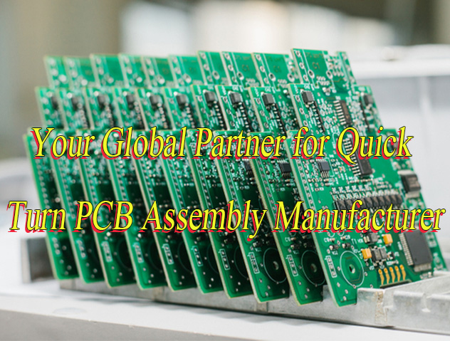
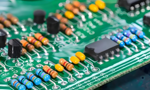
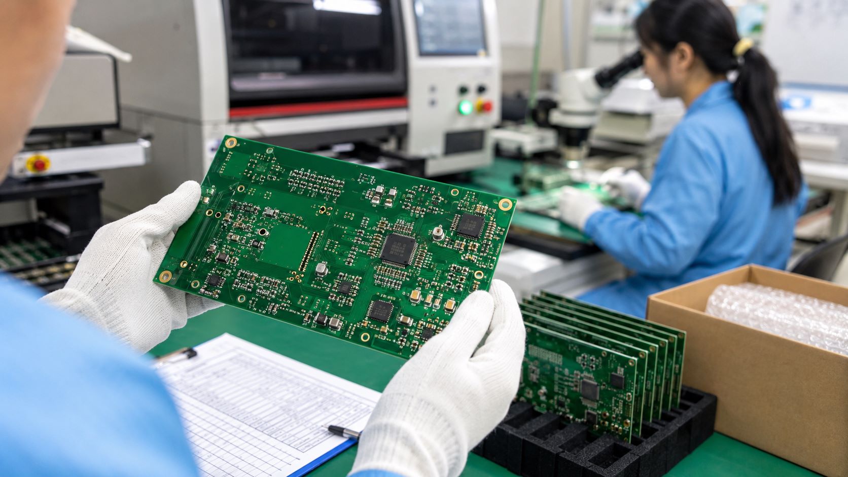
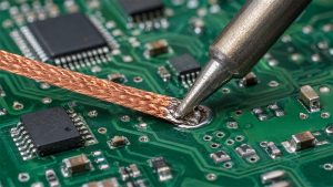
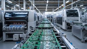
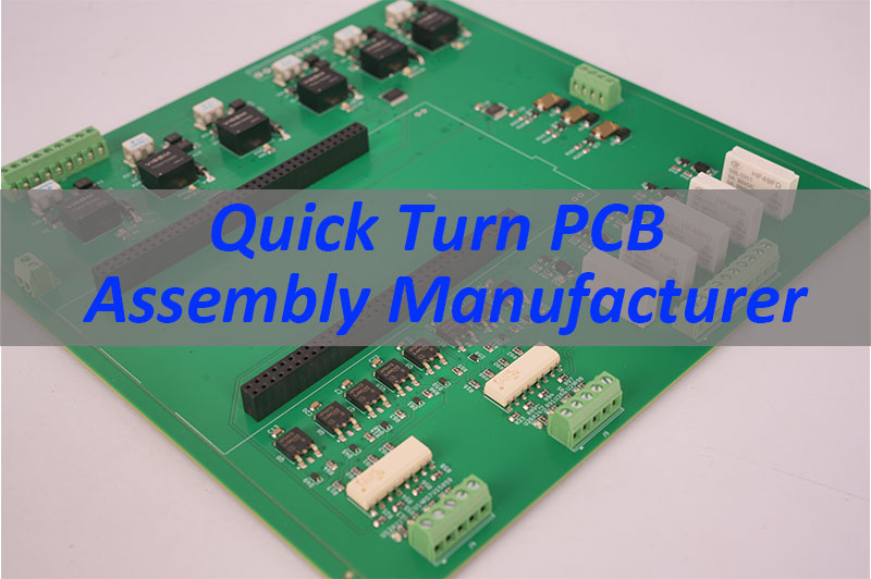
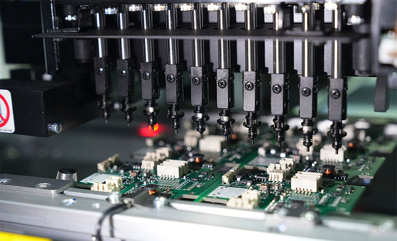
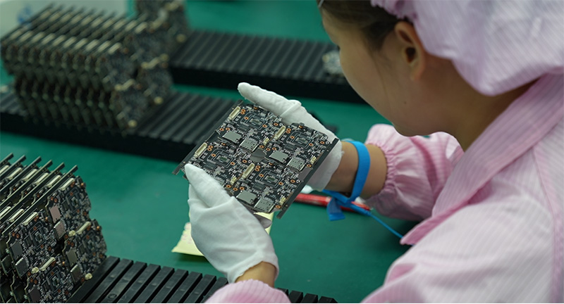
Quick turn PCB assembly manufacturer selection is not only about finding the fastest supplier; it is about choosing a partner that can turn your PCB files into reliable assembled boards with fewer delays, fewer sourcing risks, and fewer production surprises. For engineers, startups, and OEM buyers, quick-turn PCBA is often needed for functional testing, pilot runs, certification samples, investor demos, urgent design revisions, or low-volume production. A capable manufacturer should support PCB fabrication, BOM review, component sourcing, SMT assembly, through-hole assembly, inspection, testing, and delivery under one controlled workflow.
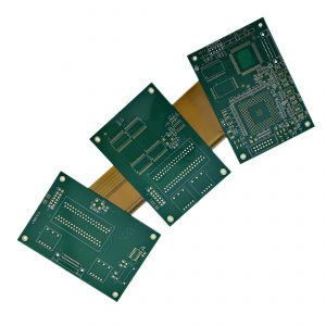
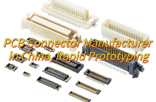
China has become a strong destination for quick turn PCB assembly because its PCB supply chain is complete, component sourcing is efficient, and low-volume production is highly flexible. However, not every supplier is suitable for time-sensitive or quality-critical projects. This guide compares the top 10 quick turn PCB assembly manufacturers in China to help you understand each company’s services, strengths, industries served, and certifications. If your project requires fast response, engineering support, reliable assembly quality, and one-stop PCB-to-PCBA service, EBest Circuit (Best Technology) is a practical partner to consider.
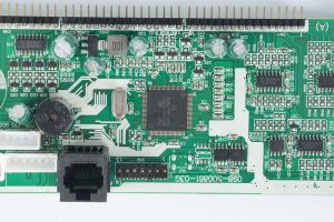
1. EBest Circuit (Best Technology)
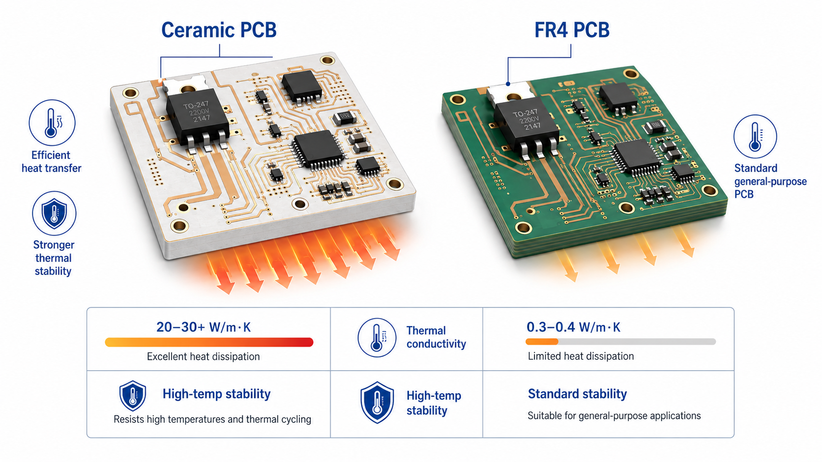
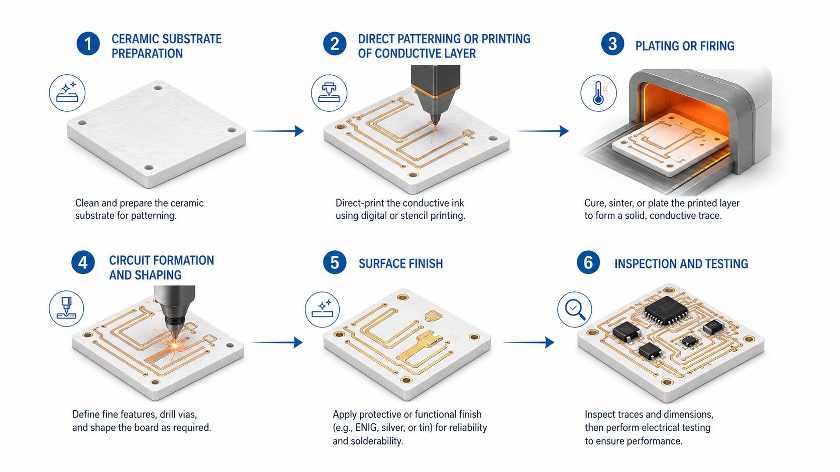
EBest Circuit (Best Technology) is a professional PCB and PCBA manufacturer in China with strong capability in quick turn prototypes, small-batch PCB assembly, and advanced PCB manufacturing. The company supports a wide range of PCB types, including FR4 PCB, metal core PCB, ceramic PCB, heavy copper PCB, extra-thin PCB, rigid-flex PCB, and PCB assembly. For PCB layout, prototyping, ODM, DFM, PCB assembly, and box building services, pls feel free to contact us via sales@bestpcbs.com.
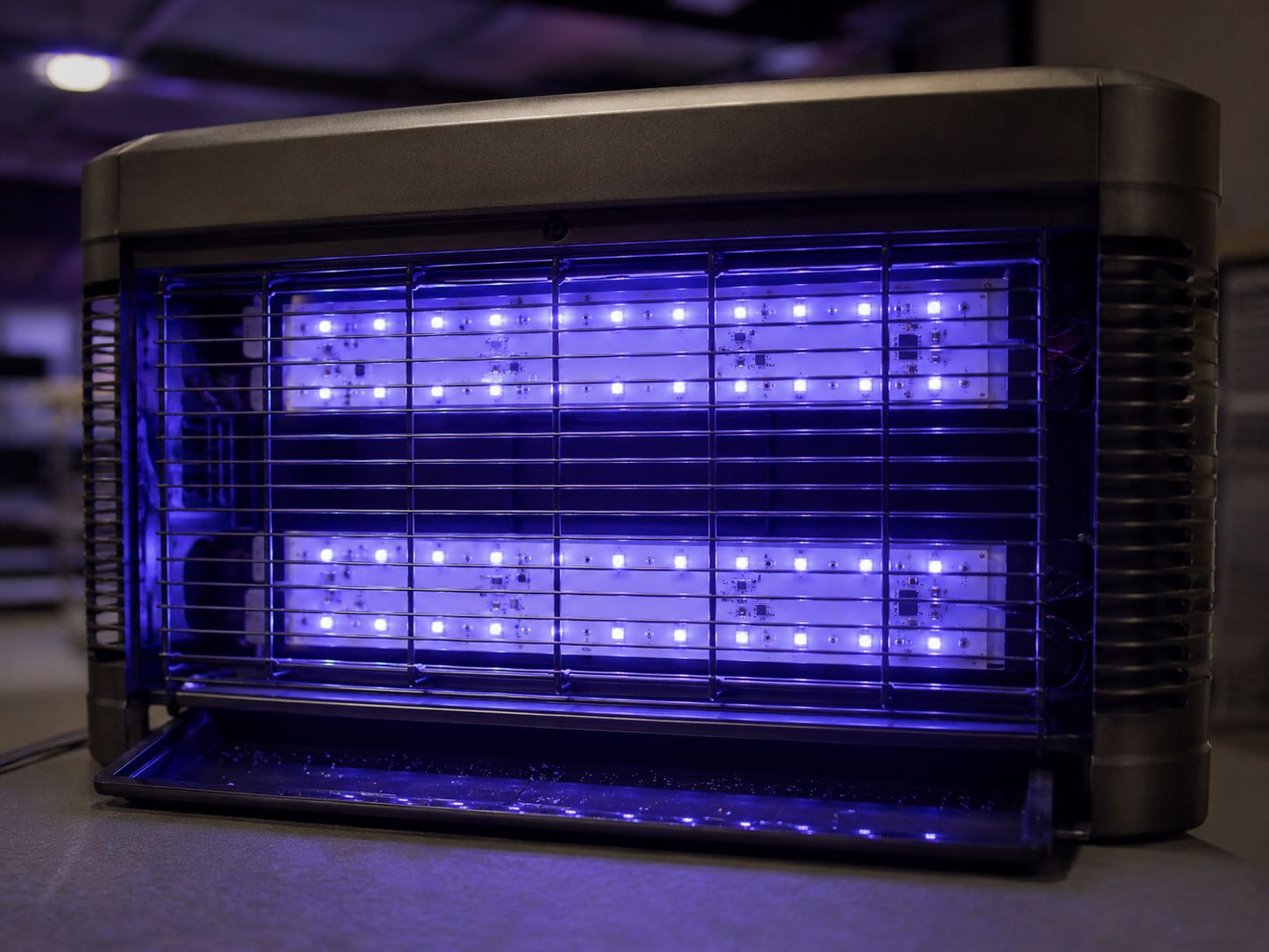
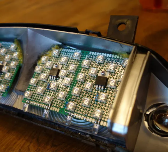
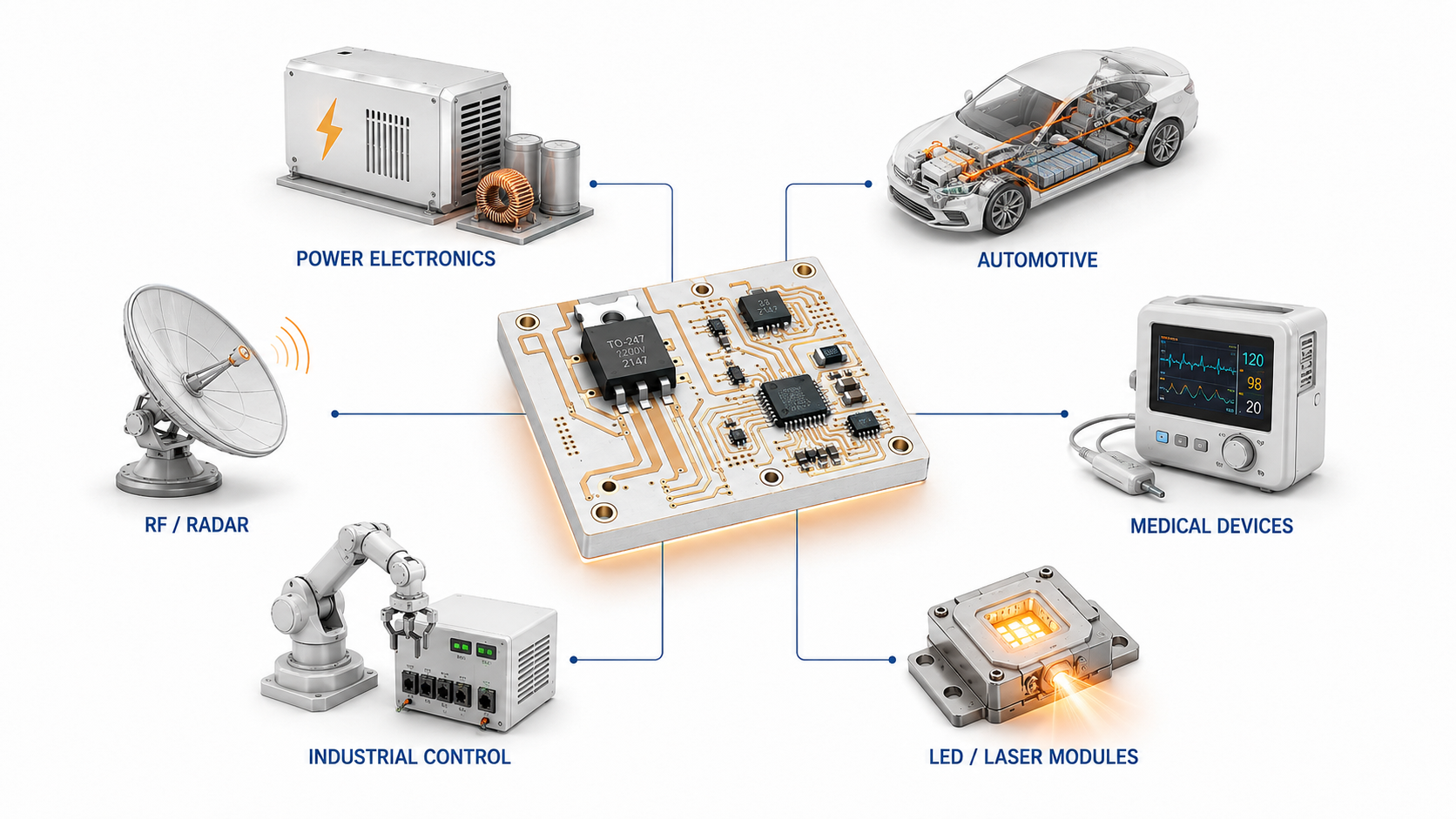
For customers looking for a China quick turn PCB assembly manufacturer, EBest Circuit is a practical option because it combines PCB fabrication, component sourcing, SMT assembly, testing, and engineering support. This is especially helpful for projects where the customer needs more than a bare PCB, such as medical electronics, automotive modules, LED lighting products, industrial control boards, communication devices, and high-reliability prototypes.
Location: Shenzhen, Guangdong, China
Services:
- PCB prototyping
- Quick turn PCB assembly
- SMT assembly
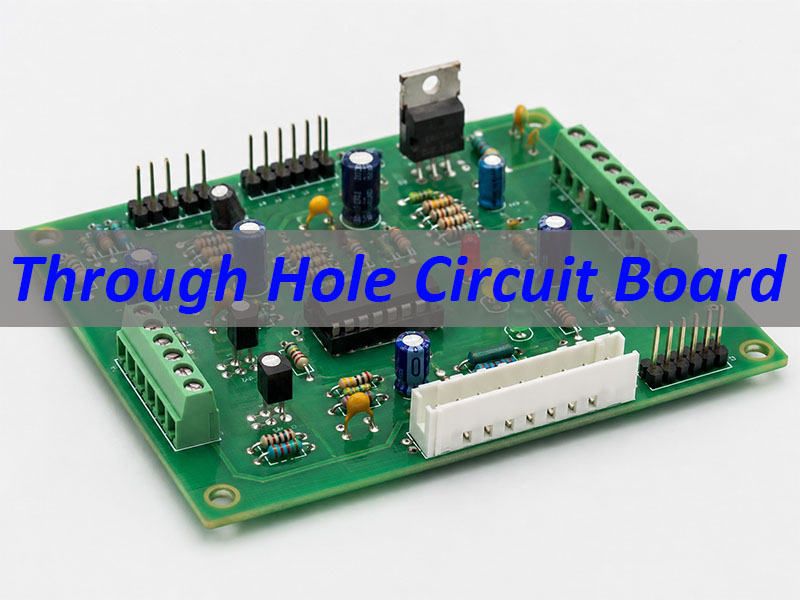
- Through-hole assembly
- Mixed assembly
- BOM sourcing
- DFM and engineering support
- Ceramic PCB manufacturing
- Metal core PCB manufacturing
- Rigid-flex PCB and flexible PCB
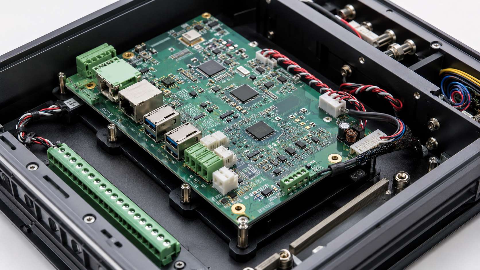
- Box build assembly
Industries Served: Medical, automotive, aerospace, industrial control, LED lighting, communication, consumer electronics, and power electronics
Key Differentiators:
- Strong one-stop PCB and PCBA service
- Quick turn prototype and small-batch assembly support
- Advanced PCB options including ceramic PCB, MCPCB, heavy copper PCB, and rigid-flex PCB
- Engineering-driven DFM support before production
- Suitable for customers who need both prototype speed and production reliability
- Broad certification coverage for regulated or high-reliability industries
Certifications:
- IATF 16949
- ISO 9001:2015
- ISO 13485:2016
- AS9100D
- UL
- RoHS
- REACH
2. FS Circuits
FS Circuits is a China-based PCB and PCBA manufacturer offering PCB prototyping, PCB manufacturing, component procurement, turnkey PCB assembly, SMT assembly, THT assembly, small-volume PCB assembly, and conformal coating. Its website describes the company as an ISO-certified PCBA provider with more than 15 years of industrial experience, 8 SMT lines, 2 THT lines, and support for 0201 components and 0.4mm BGA pitch.
For buyers comparing quick turn PCB assembly manufacturers, FS Circuits is relevant because it provides both fabrication and assembly under one supplier. Its service pages also mention testing and packaging, which are important for customers who need a finished PCBA instead of only bare boards.
Location: Shenzhen, Guangdong, China
Services:
- PCB prototyping
- PCB manufacturing
- Turnkey PCB assembly
- SMT PCB assembly
- THT PCB assembly
- Small-volume PCB assembly
- Component procurement
- Testing and packaging
- Conformal coating
Industries Served: IoT, industrial control, aerospace, telecommunications, medical, automotive, security systems, computer equipment, new energy, and smart home
Key Differentiators:
- One-stop PCB and PCBA manufacturing service
- 8 SMT lines and 2 THT lines
- Support for fine-pitch components and BGA assembly
- Material procurement, PCB production, PCBA assembly, testing, and packaging
- Suitable for prototype and small-volume production
- Factory address publicly listed in Shenzhen
Certifications:
- ISO9000
- ISO9001
- ISO14001
- UL
- TS16949
- UL/CE export standards
3. NextPCB
NextPCB is a well-known PCB manufacturing and assembly provider in China, offering turnkey PCB assembly, prototype PCBA, component sourcing, DFM/DFA review, testing, and order tracking. Its PCB assembly page highlights assembly launch within 24 hours once parts are confirmed, superfast turnkey PCBA from 7 working days, access to a large verified component inventory, and global shipping support.
NextPCB is suitable for engineers and hardware teams that need an online ordering process, structured file review, and clear assembly workflow. It is also a strong option for customers who need Rev 0 prototypes, BOM handling, and scalable PCB assembly from prototype to higher-volume production.
Location: Shenzhen, Guangdong, China
Services:
- PCB fabrication
- Turnkey PCB assembly
- Prototype PCBA
- BOM handling
- Component sourcing
- SMT assembly
- THT and mixed assembly
- Rigid-flex PCB integration
- DFM/DFA review
- AOI and X-ray inspection
- ICT, flying probe, and functional circuit testing
Industries Served: Aerospace, medical electronics, consumer electronics, industrial electronics, communication, and hardware development
Key Differentiators:
- Free DFM/DFA review for orders
- Zero MOQ for PCB assembly
- Component sourcing support
- Real-time order tracking
- AOI and X-ray inspection support
- Functional testing available on request
- Good fit for online prototype and engineering projects
Certifications:
- ISO 9001
- UL
- IATF 16949
- RoHS
- REACH
- IPC-A-610 quality control practices mentioned on its assembly service page
4. Swimbi
Swimbi presents itself as an electronic manufacturing service company focused on high-end engineering, PCB manufacturing, and SMT assembly. Its website positioning is concise, but it clearly places PCB manufacturing and SMT assembly as core services.
For buyers searching for a quick turn PCB assembly manufacturer, Swimbi may be considered when the project needs EMS-style support rather than only PCB fabrication. Since its public website provides limited details compared with larger PCB platforms, buyers should confirm factory location, lead time, testing process, and certification documents before placing urgent orders.
Location: Public factory address not clearly listed on the reviewed page
Services:
- PCB manufacturing
- SMT assembly
- Electronic manufacturing services
- Engineering support
Industries Served: Electronics engineering, prototype development, industrial electronics, and customized EMS projects
Key Differentiators:
- EMS positioning
- Focus on engineering-oriented electronic manufacturing
- PCB manufacturing and SMT assembly support
- Suitable for buyers who want to discuss customized production requirements
Certifications:
- UL
5. Wintech Technology
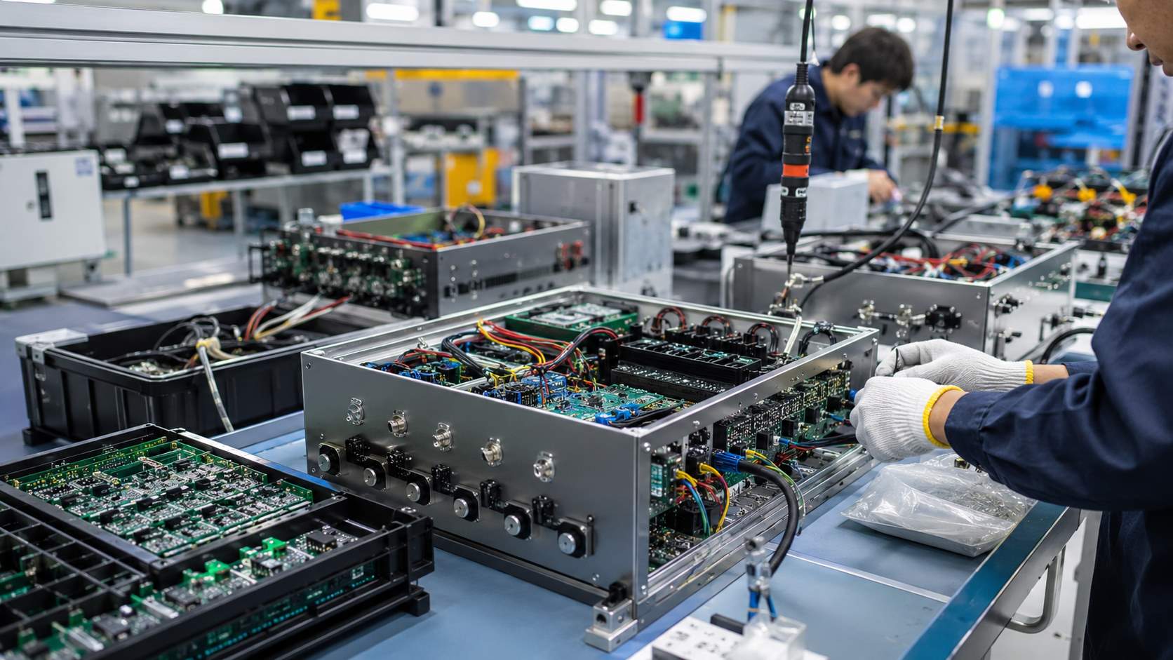
Wintech Technology is a China-based electronic contract manufacturer that supports PCB assembly, SMT assembly, through-hole assembly, box build, and full system integration. Its website states that Wintech specializes in contract manufacturing of electronic assemblies, from prototypes to small and medium production volumes. It also serves markets such as industrial controls, medical instruments, defense, aerospace, automotive, energy, oil and gas, and consumer electronics.
Wintech is a useful option for customers who need a quick turn PCB assembly manufacturer with broader EMS capability. In addition to PCB assembly, its public information mentions PCB fabrication, electro-mechanical assembly, mechanical tooling, plastic injection molding, metal stamping, die-casting, final box build assembly, full system integration, function testing, and burn-in.
Location: Shenzhen, Guangdong, China
Services:
- PCB design and layout
- PCB manufacturing
- PCB assembly and PCBA SMT
- Quick turn PCB prototype service
- Through-hole assembly
- Box build assembly
- Full system integration
- Function testing
- Burn-in testing
- New product introduction support
Industries Served: Industrial control, medical devices, defense, aerospace, automotive electronics, energy, oil and gas, consumer electronics, clean technology, communication, computing, and storage
Key Differentiators:
- EMS and contract manufacturing experience
- Prototype to small and medium production volume support
- SMT, through-hole, box build, and full system integration
- Strong fit for customers who need complete product assembly, not only PCB assembly
- Engineering support for NPI and DFM
Certifications:
- ISO13485
- ISO16949
6. LHD Technology
LHD Technology, also shown as LHD TECH or LHDPCB, provides PCB fabrication and PCB assembly from prototype design to mass production. Its website describes the company as a one-stop PCB assembly manufacturer with professional PCB fabrication, rapid prototyping, a component supply chain, more than 20 years of experience, and customized assembly solutions.
LHD is relevant for customers seeking quick turn PCB assembly because it lists quick turn PCB assembly, turnkey PCB assembly, through-hole PCB assembly, HDI PCB, flexible PCB, heavy copper PCB, multilayer PCB, and Rogers PCB among its products and services. It also highlights factory locations in Shenzhen, Zhuhai, and Jiangxi, China.
Location: Shenzhen, Zhuhai, and Jiangxi, China
Services:
- PCB fabrication
- Quick turn PCB assembly
- Turnkey PCB assembly
- Through-hole PCB assembly
- Component sourcing
- HDI PCB
- Flexible PCB
- Heavy copper PCB
- Multilayer PCB
- Rogers PCB
- Testing and shipping support
Industries Served: Aerospace, industrial electronics, medical electronics, robotics, drones, IoT, communication, and custom electronics
Key Differentiators:
- One-stop PCB assembly service
- Rapid prototyping support
- Factory locations in multiple Chinese manufacturing regions
- Component sourcing support
- PCBs up to 64 layers mentioned on its public page
- Engineering and one-on-one service support
Certifications:
- ISO
- UL
- RoHS
7. PCBTok
PCBTok is a PCB and PCB assembly service manufacturer in China. Its website states that the company can offer quick-turn PCB fabrication, including 24-hour prototypes for single-sided and double-sided boards and 48-hour service for multilayer boards. It also provides turnkey PCB assembly from prototype to medium and large-volume production.
PCBTok is suitable for customers who need PCB fabrication, PCB layout support, electronic component sourcing, and assembly under one supplier. Its public page also lists SMT assembly, BGA assembly, through-hole assembly, mixed assembly, and other PCB assembly services.
Location: Ganzhou, Jiangxi Province, China
Services:
- Quick turn PCB fabrication
- PCB assembly
- Turnkey PCB assembly
- SMT assembly
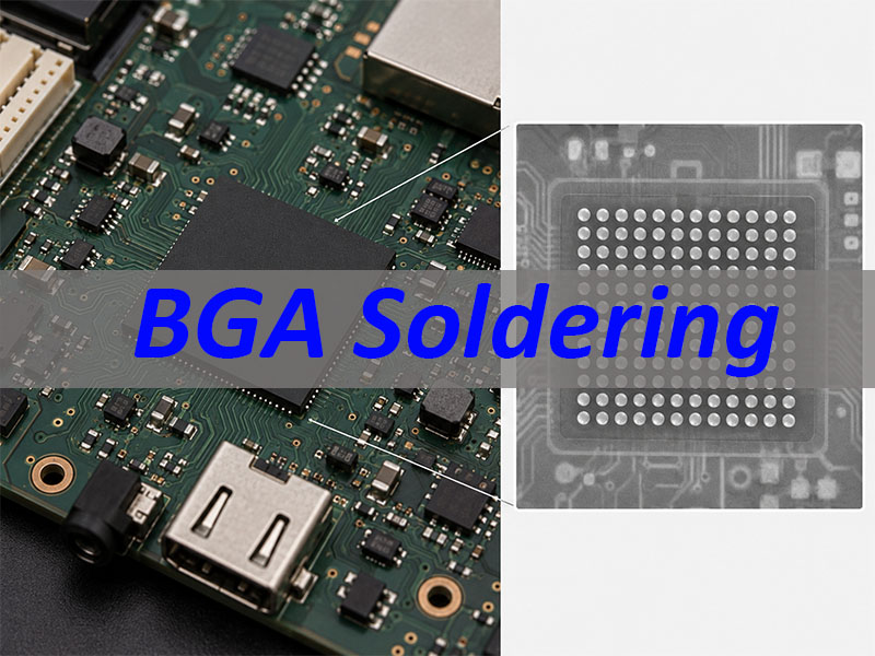
- BGA assembly
- Through-hole assembly
- Mixed assembly
- PCB layout and design
- Electronic component sourcing
- Prototype to volume production support
Industries Served: Industrial electronics, consumer electronics, communication, power electronics, custom hardware, and electronic product development
Key Differentiators:
- 24-hour prototype support for simple PCB types
- 48-hour multilayer PCB support
- Turnkey PCB assembly service
- Electronic component sourcing support
- PCB layout and design assistance
- Suitable for prototype, medium-quantity, and large-volume orders
Certifications:
- ISO9001:2015
- ISO14001:2015
- USA UL
- Canada UL
- REACH
- RoHS
8. RAYPCB
RAYPCB, also known as Rayming Technology, is a Chinese PCB and PCBA manufacturer offering rapid PCB prototyping and complete turnkey assembly services. Its website describes full turnkey PCBA services, premium PCB manufacturing, reliable PCB assembly, authentic component procurement, and advanced PCBA testing and quality control.
RAYPCB is a strong candidate for customers who need a quick turn PCB assembly manufacturer with experience in end-to-end manufacturing. It can be considered for projects that need PCB production, component sourcing, PCBA assembly, testing, and engineering communication under one workflow.
Location: China
Services:
- PCB manufacturing
- Rapid PCB prototyping
- Turnkey PCB assembly
- Component procurement
- PCBA testing
- Quality control
- Prototype and production support
Industries Served: Industrial electronics, communication, automotive electronics, medical electronics, power electronics, consumer electronics, and custom electronic products
Key Differentiators:
- End-to-end PCB and PCBA service
- Rapid prototyping support
- Turnkey assembly with component procurement
- Advanced PCBA testing and quality control
- Suitable for customers who need one supplier for fabrication, sourcing, and assembly
Certifications:
- ISO 9001
- IATF 16949
9. Unit Circuits
Unit Circuits is a China-based EMS provider specializing in turnkey PCB assembly, PCB manufacturing, component sourcing, SMT/THT assembly, testing, and global shipping. Its website states that it supports startups, hardware engineers, and OEM brands with flexible MOQ, fast delivery, and reliable quality.
For quick turn projects, Unit Circuits is especially relevant because its public FAQ says the company supports quick-turn PCB production, with PCB bare boards in 1–3 working days and turnkey PCB assembly in 5–10 days. It also states that the company has no MOQ requirements and supports prototypes, small batches, and growing production volumes.
Location: Shenzhen, Guangdong, China
Services:
- PCB assembly
- PCB manufacturing
- Component procurement
- SMT assembly
- Through-hole assembly
- BGA assembly
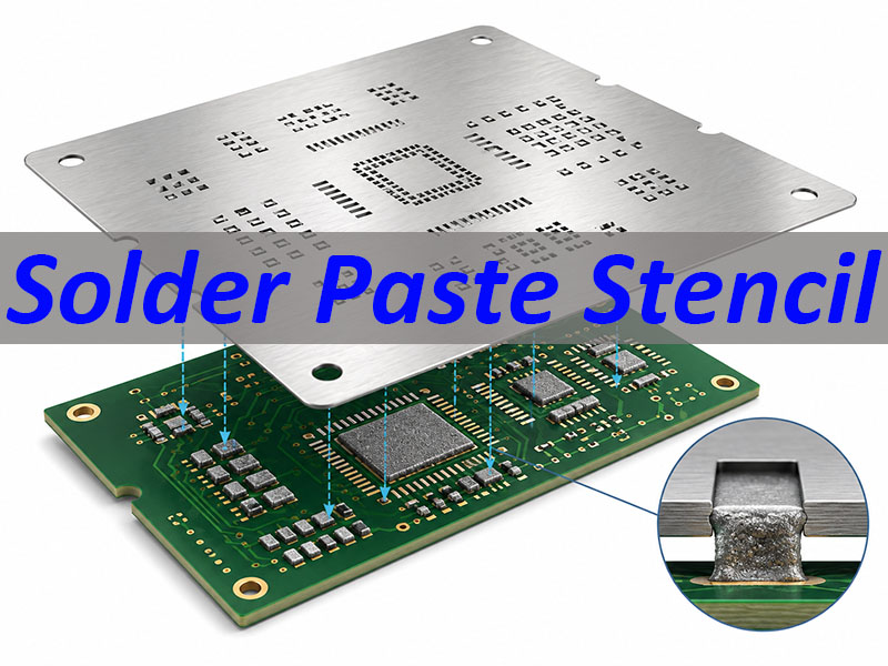
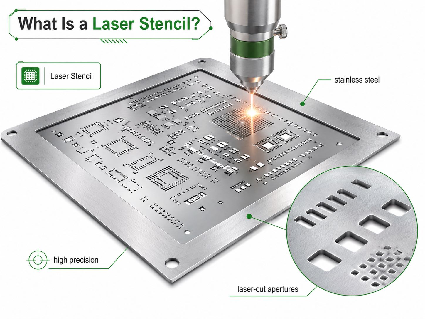
- PCBA stencil
- Function testing
- Box-build assembly
- Electronics product development
- DFM and DFA support
Industries Served: Startups, hardware engineering teams, OEM electronics brands, industrial electronics, consumer electronics, communication, smart devices, and low-to-medium volume manufacturing
Key Differentiators:
- No MOQ requirements
- Quick-turn PCB production support
- Turnkey PCB assembly in 5–10 days for suitable projects
- PCB bare boards in 1–3 working days
- SMT, through-hole, BGA, and box-build support
- DFM/DFA engineering assistance
- Factory and office address publicly listed in Shenzhen
Certifications:
- UL
- ISO9001:2015
- RoHS
- REACH
- IPC Class 2/3 support
10. PCBGOGO
PCBGOGO is a PCB prototype and PCB assembly manufacturer in China. Its website states that it has offered PCB and PCB assembly service worldwide since 2015 and specializes in quick-turn PCB prototyping and turnkey PCB assembly. The site also lists 24/48-hour expedited manufacturing for FR4 prototype PCBs and PCB assembly support with component sourcing.
PCBGOGO is suitable for engineers, hobbyists, startups, and product developers who need fast PCB prototypes, small-volume PCBA, online quotation, PCB assembly, and component sourcing. Its platform-style ordering process makes it convenient for customers who already have Gerber, BOM, and pick-and-place files ready.
Location: China
Services:
- PCB prototype manufacturing
- Quick-turn PCB prototype service
- PCB assembly
- Turnkey SMT assembly
- Component sourcing
- SMT stencil
- Flexible PCB
- Rigid-flex PCB
- Aluminum PCB
- Copper PCB
- Rogers PCB
- Online PCB and PCBA quotation
Industries Served: Electronics engineers, hardware startups, hobbyist projects, consumer electronics, IoT, industrial electronics, LED products, and custom electronic devices
Key Differentiators:
- Quick-turn prototype PCB service
- Turnkey PCB assembly support
- Low minimum order quantity for PCB assembly
- Component sourcing available
- Online quotation and order tracking
- Suitable for prototype and small-volume assembly orders
Certifications:
- ISO9001
- UL
- RoHS
11. FAQs About Quick Turn PCB Assembly Manufacturer
Q1: What is a quick turn PCB assembly manufacturer?
A quick turn PCB assembly manufacturer is a supplier that can complete PCB fabrication, component sourcing, SMT assembly, through-hole assembly, inspection, testing, and delivery within a shorter production cycle than standard PCBA services. These manufacturers are often used for prototypes, engineering validation, urgent samples, and low-volume production.
Q2: Why choose a China quick turn PCB assembly manufacturer?
China has a mature PCB and electronics manufacturing supply chain. Many Chinese manufacturers can provide PCB fabrication, BOM sourcing, SMT assembly, testing, and shipping in one place. This can help reduce communication time, sourcing delays, and total prototype cost.
Q3: What files are needed for a quick turn PCB assembly quote?
Most manufacturers need Gerber files, BOM, pick-and-place files, assembly drawings, PCB specifications, quantity, testing requirements, and any special instructions. If the project includes programmed ICs, conformal coating, box build, or functional testing, those details should be provided at the RFQ stage.
Q4: How fast can quick turn PCB assembly be completed?
Lead time depends on PCB complexity, component availability, assembly difficulty, testing requirements, and order quantity. Simple bare PCB prototypes may be completed within 24 to 72 hours by some suppliers. Full PCBA usually takes longer because it includes BOM checking, component sourcing, SMT setup, assembly, inspection, and testing.
Q5: What is the difference between quick turn PCB manufacturing and quick turn PCB assembly?
Quick turn PCB manufacturing refers to producing the bare printed circuit board. Quick turn PCB assembly refers to mounting electronic components onto the PCB to create a functional PCBA. Assembly usually requires more preparation because the manufacturer must review the BOM, source components, prepare SMT machines, inspect soldering quality, and run tests.
Q6: Is quick turn PCB assembly suitable for startups?
Yes. Startups often need fast PCBA samples for product testing, investor demos, certification preparation, crowdfunding validation, and early customer trials. A good quick turn PCB assembly manufacturer can help startups move from design files to working prototypes faster.
Q7: Can quick turn PCB assembly manufacturers support low-volume orders?
Many Chinese PCB assembly manufacturers support prototypes, small batches, and low-volume production. Some suppliers offer no MOQ or very low MOQ options, which is useful when the product is still under development or market demand is not yet stable.
Q8: What affects the lead time of quick turn PCB assembly?
The main factors include PCB layer count, surface finish, material type, component stock, BOM accuracy, BGA or fine-pitch components, stencil preparation, testing requirements, conformal coating, programming, packaging, and shipping method. In most urgent orders, component availability is one of the biggest lead-time risks.
Q9: How can I choose a reliable quick turn PCB assembly manufacturer?
Check whether the supplier offers DFM review, BOM checking, component sourcing, SMT and THT assembly, AOI, X-ray inspection, functional testing, quality traceability, and clear communication. Also review certifications such as ISO9001, ISO13485, IATF16949, UL, RoHS, and REACH when your product requires compliance.
Q10: Why should buyers consider EBest Circuit (Best Technology) for quick turn PCB assembly?
EBest Circuit is suitable for customers who need fast PCB prototyping, low-volume PCB assembly, advanced PCB manufacturing, and one-stop engineering support. Its strengths include FR4 PCB, ceramic PCB, metal core PCB, heavy copper PCB, rigid-flex PCB, SMT assembly, BOM sourcing, DFM support, and broad certifications for medical, automotive, aerospace, and industrial applications.
To conclude, choosing the right quick turn PCB assembly manufacturer is not only about finding the fastest supplier. A reliable partner should also understand your PCB design, review your BOM, check manufacturability, source correct components, control SMT quality, inspect solder joints, and deliver working PCB assemblies on time.
For buyers searching for a China quick turn PCB assembly manufacturer, the companies listed above offer different strengths. Some are strong in online prototype ordering, some focus on turnkey PCBA, and others provide broader EMS or advanced PCB support. If your project requires fast delivery, low-volume production, engineering support, and high-reliability PCB capability, EBest Circuit (Best Technology) can help you move from prototype to production with a more controlled and efficient process. To discuss your PCB assembly project or request a fast quotation, pls feel free to contact us at sales@bestpcbs.com.