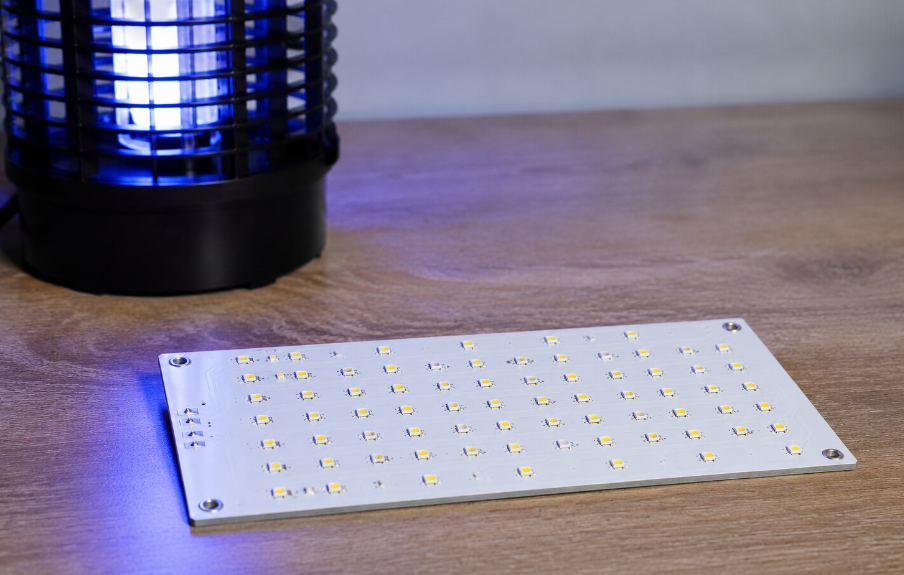
Metal-core PCB fabrication for LED insect light traps focuses on heat dissipation, UV LED stability, and long service life. These products often run for 8–12 hours per night in humid, dusty, or semi-outdoor environments. Poor heat transfer can reduce UV output, shift LED wavelength, weaken solder joints, and shorten product life.
A reliable metal-core PCB fabrication project should match the LED power, housing structure, working voltage, and target environment. Key specifications include aluminum or copper core, copper thickness, thermal dielectric, white solder mask, surface finish, insulation testing, and assembly quality control.
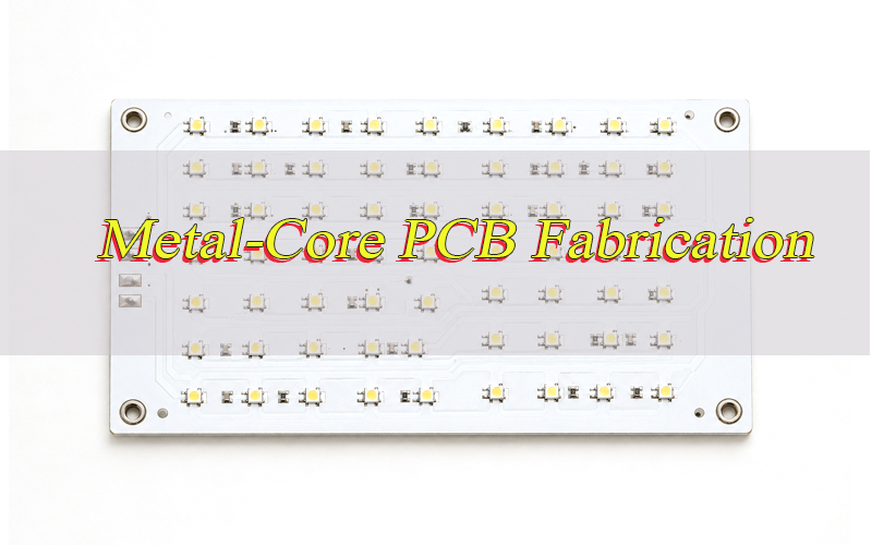
Why Does Metal-Core PCB Fabrication Matter for LED Insect Light Traps?
LED insect light traps use metal-core PCB because UV LEDs generate concentrated heat around the LED pads. FR-4 PCB is suitable for low-power control circuits, but it transfers heat slowly. MCPCB moves heat from the LED solder pad through copper, thermal dielectric, and metal base into the housing or heat sink.
Good metal-core PCB fabrication helps control heat before it damages LED output or solder joints.
Key reasons include:
- Faster heat transfer: FR-4 thermal conductivity is usually around 0.3 W/m·K, while MCPCB dielectric commonly reaches 1.0–5.0 W/m·K.
- More stable UV output: Lower LED temperature helps reduce brightness decay during long operation.
- Lower wavelength drift: UV LED wavelength can shift when junction temperature rises.
- Longer solder joint life: Lower thermal stress reduces pad fatigue and solder cracking.
- Better LED consistency: Uniform heat spreading helps keep brightness more even across the LED array.
- Stronger board structure: Aluminum MCPCB supports long strips, round boards, and custom trap modules better than thin FR-4.
Common UV wavelengths for insect traps include 365 nm, 385 nm, 395 nm, and 405 nm.
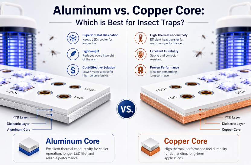
Aluminum vs. Copper Core: Which is Best for Insect Traps?
Aluminum core is suitable for most LED insect light traps, while copper core is mainly used for compact high-power UV LED modules. Aluminum offers enough thermal performance for most commercial trap boards and keeps cost, weight, and processing difficulty under control. Copper spreads heat faster, but it increases material cost and machining difficulty.
| Factor | Aluminum Core | Copper Core |
|---|---|---|
| Thermal Conductivity | 150–220 W/m·K | 380–400 W/m·K |
| Heat Spreading | Good for most UV LED trap boards | Stronger for dense high-power LED layouts |
| Weight | Lighter, better for hanging and wall-mounted traps | Heavier, less suitable for lightweight housings |
| Material Cost | Lower and easier for mass production | Higher, used for premium or special projects |
| Processing Difficulty | Easier drilling, routing, and profiling | Harder machining and stricter control |
| Board Thickness | Commonly 1.0–2.0 mm | Commonly 1.0–2.0 mm |
| Copper Thickness Match | Usually 1 oz–2 oz copper | Often matched with 2 oz–3 oz copper |
| Dielectric Match | 1.0–3.0 W/m·K is common | 2.0–5.0 W/m·K is preferred |
| Typical Application | Mosquito traps, fly traps, warehouse traps, agricultural trap lights | Compact UV modules, high-power trap lamps, sealed metal housings |
| Production Stability | Strong for prototype and mass production | Depends on factory MCPCB process control |
| Cost Performance | Best for most insect trap projects | Best when thermal risk is higher than material cost |
| Recommended Use | Standard commercial LED insect traps | High-power or space-limited UV modules |
For most insect trap products, aluminum core provides the best balance of thermal control, cost, weight, and production stability. Copper core is worth considering only when thermal testing shows that aluminum cannot keep LED temperature within the target range.
What Copper Thickness & Thermal Conductivity Should Be Used in Metal-Core PCB Fabrication?
Most LED insect trap MCPCBs use 1 oz to 2 oz copper, 1.0–3.0 W/m·K dielectric, and 1.0–2.0 mm aluminum base thickness. These specifications cover most UV LED boards used in commercial and industrial insect trap products.
Recommended copper thickness:
- 1 oz copper: About 35 µm, suitable for low to medium-power UV LED boards.
- 2 oz copper: About 70 µm, better for higher current and wider heat spreading.
- 3 oz copper: About 105 µm, used for compact high-power LED modules.
- Above 3 oz: Usually unnecessary for standard insect traps unless current density is high.
Recommended dielectric selection:
- 1.0 W/m·K: Low-power LED boards with enough heat-dissipation space.
- 1.5–2.0 W/m·K: Common option for commercial insect trap MCPCBs.
- 3.0 W/m·K: Better for dense LED arrays or sealed housings.
- 5.0 W/m·K: Used only when thermal testing supports the added cost.
Other useful values:
- Common dielectric thickness: 75–150 µm.
- High-power dielectric thickness: 50–100 µm.
- Common breakdown voltage: 2–4 kV.
- Stricter insulation projects: 3–6 kV.
- Common aluminum base thickness: 1.0 mm, 1.5 mm, or 2.0 mm.
The right specification should match LED power, board size, enclosure material, mounting method, and cost target.
What Surface Finish Works Best in Metal-Core PCB Fabrication for LED Insect Traps?
ENIG is often preferred for LED insect light trap MCPCBs because it provides flat pads, stable solderability, and better oxidation resistance. It works well for SMT UV LEDs, export shipping, long storage, and humid environments.
Surface finish options:
- ENIG: Typical thickness is 3–6 µm nickel and 0.05–0.10 µm gold. It is suitable for fine LED pads and stable assembly.
- Lead-free HASL: Suitable for larger LED pads and cost-sensitive production, but pad flatness is weaker than ENIG.
- OSP: Low cost, but better for short storage and fast assembly.
- Immersion silver: Flat and solderable, but storage conditions must be controlled.
- ENEPIG: Used for special high-reliability requirements, usually unnecessary for standard insect traps.
Practical choice:
- Use ENIG for higher-quality UV LED trap boards.
- Use lead-free HASL when LED pads are large and cost is the main concern.
- Avoid OSP for long storage or long-distance export projects.
- Confirm surface finish before SMT assembly, because pad quality affects LED placement and soldering yield.
How Should Metal-Core PCB Fabrication Support UV LED Layout and Thermal Design?
A good UV LED trap layout should spread heat evenly, control current flow, and keep the MCPCB in firm contact with the housing. Material selection alone cannot solve poor layout. LED spacing, copper area, mounting holes, and trace width directly affect heat and brightness consistency.
Key layout rules:
- Use wide current traces: LED power traces commonly use 1.0–3.0 mm width, depending on current.
- Avoid narrow copper necks: Narrow copper near LED pads increases local temperature.
- Balance LED strings: Uneven current causes brightness difference and faster aging.
- Keep LED spacing consistent: Irregular spacing creates hot spots and uneven light output.
- Add copper around LED pads: Larger copper areas improve heat spreading before heat enters the dielectric.
- Place mounting holes near heat areas: Better contact helps move heat into the housing.
- Control solder mask clearance: Common LED pad clearance is 0.10–0.20 mm.
- Mark LED polarity clearly: This reduces SMT placement errors.
- Check creepage and clearance: AC-input or high-voltage trap modules require stricter spacing review.
Useful design targets:
- LED temperature difference across the board: within 5–10°C where possible.
- Board warpage target: below 0.75%.
- Thermal interface material thickness: commonly 0.1–0.3 mm.
- High-current paths: short, wide, and direct.
Why Is High-Reflectivity White Solder Mask Critical for UV LED Traps?
High-reflectivity white solder mask improves light use and makes LED assembly defects easier to inspect. In insect trap modules, the PCB surface is close to the LED light path. Low-quality solder mask can absorb more heat, discolor under UV exposure, and reduce product appearance.
Main functions:
- Reflects more light: White solder mask reflects better than green, black, or red solder mask.
- Reduces local heat absorption: A reflective surface helps limit heat buildup around LED pads.
- Improves inspection: LED polarity, solder joints, stains, and scratches are easier to see.
- Supports clean product design: White MCPCB matches most LED trap housings and light modules.
Technical points:
- Common solder mask thickness: 15–30 µm.
- Reflow heat resistance: around 260°C short-cycle exposure.
- The ink should resist yellowing after UV and heat exposure.
- Adhesion should remain stable after humidity and temperature cycling.
- Matte or semi-gloss white is easier to inspect than high-gloss white.
For UV LED trap MCPCBs, solder mask quality affects both appearance and reliability.
Harsh Environment Challenges: Reliability & Testing for Insect Trap MCPCBs
LED insect trap MCPCBs should withstand heat, humidity, dust, insects, vibration, and repeated temperature changes. These boards are often used in farms, warehouses, food areas, gardens, livestock facilities, and semi-outdoor installations.
Common reliability risks:
- Thermal fatigue: Heating and cooling cycles can crack LED solder joints.
- Moisture leakage: Weak insulation may increase leakage current in humid areas.
- Pad oxidation: Poor surface finish or packaging affects solderability.
- White mask yellowing: Low-grade solder mask can discolor under UV and heat.
- Edge burrs: Aluminum burrs can affect mounting and insulation safety.
- Dielectric scratches: Damage to the insulation layer may create electrical risk.
- Board warpage: Long strip boards may lose contact with the heat sink.
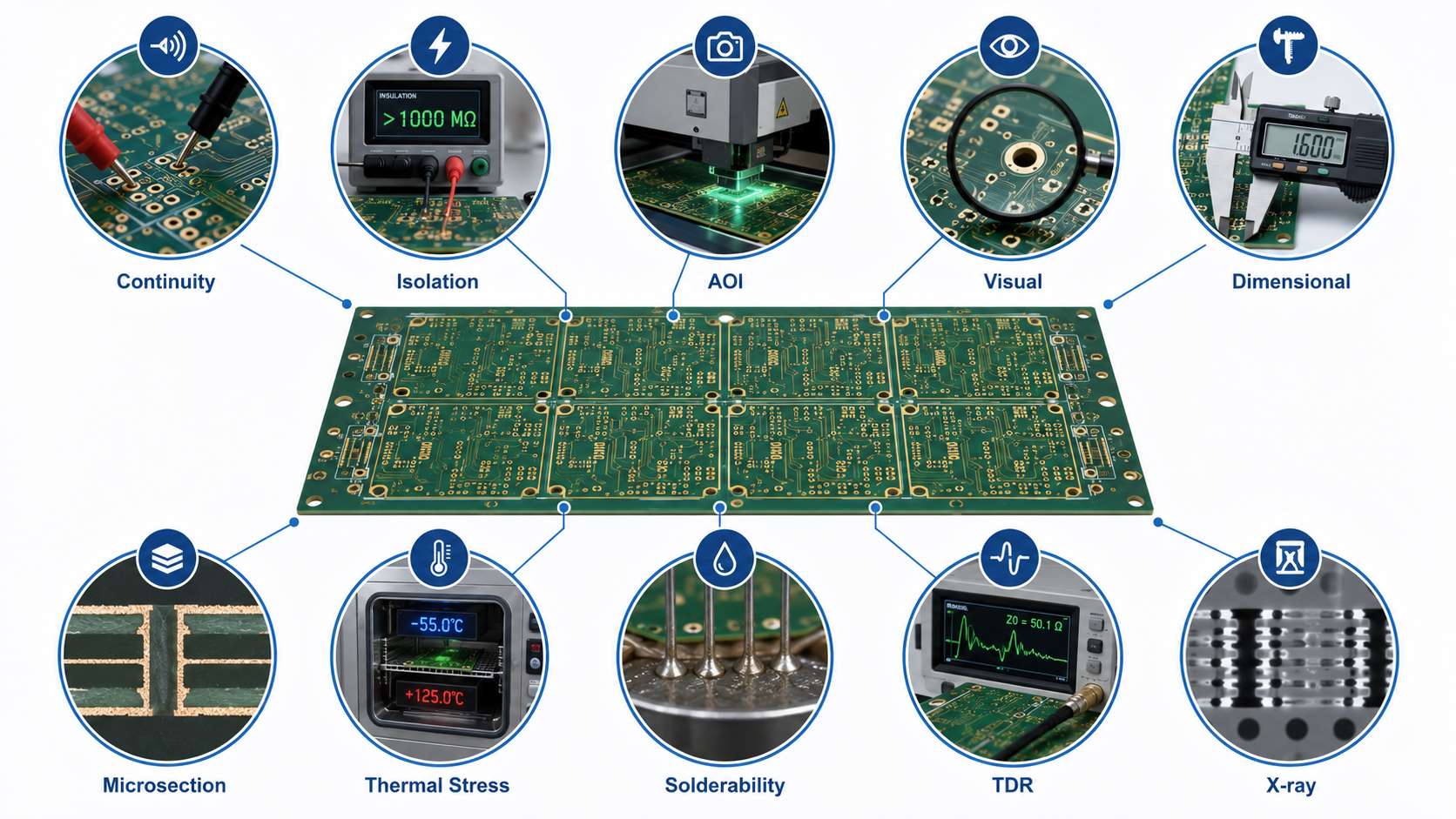
Recommended testing:
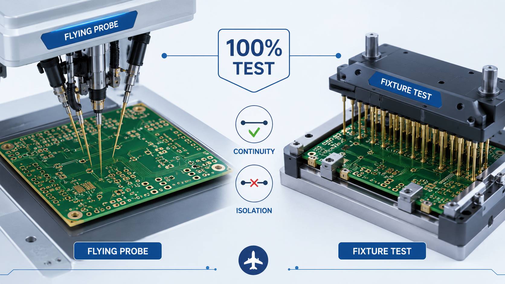
- 100% E-test for open and short circuits.
- Hi-pot test at 500–1500 VDC when insulation safety is important.
- Thermal cycling from -40°C to +85°C for demanding outdoor products.
- Humidity test at 85°C/85%RH for 500–1000 hours for high-reliability projects.
- Solderability test around 245–260°C.
- UV exposure test for 72–168 hours to check solder mask discoloration.
- Lighting test for 4–24 hours after assembly.
- Final visual inspection for burrs, scratches, pad oxidation, stains, and solder mask defects.
A practical failure example:
- A 24 W UV LED trap board showed uneven brightness after continuous operation.
- The center LEDs ran hotter because copper spreading and housing contact were weak.
- After changing to 2 oz copper and improving mounting contact, the board temperature difference dropped below 8°C.
How Does Metal-Core PCB Fabrication Reduce UV LED Thermal Decay and Wavelength Shift?
MCPCB reduces UV LED thermal decay by shortening the heat path from the LED pad to the metal housing. When UV LEDs run hot, light output drops faster and wavelength stability becomes worse. This directly affects insect attraction over time.
Thermal path:
- Heat starts from the LED chip.
- It moves to the LED thermal pad and solder joint.
- Copper spreads heat across the circuit layer.
- Thermal dielectric transfers heat into the metal base.
- Aluminum or copper base spreads heat to the housing.
- The housing releases heat into the surrounding air.
Useful control targets:
- LED board surface temperature: below 70°C where possible.
- LED array temperature difference: within 5–10°C.
- Thermal validation time: 4–24 hours.
- Thermal interface material thickness: 0.1–0.3 mm.
- Temperature measurement point: after the product reaches thermal balance.
MCPCB works together with housing design, screw pressure, thermal pad contact, LED spacing, airflow, and power control. A good board cannot fully compensate for a poor enclosure.
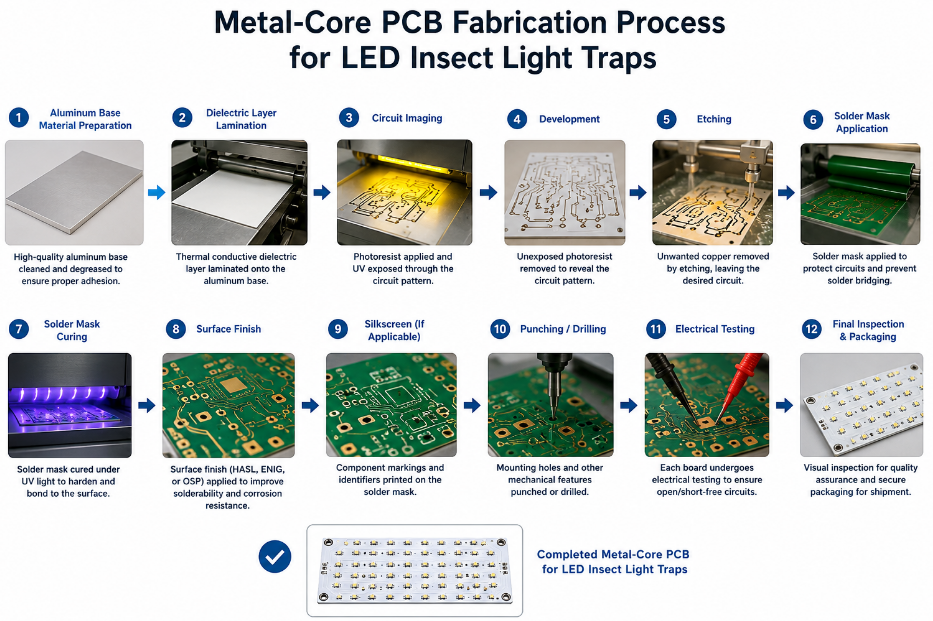
What Is the Metal-Core PCB Fabrication Process for LED Insect Light Traps?
The metal-core PCB fabrication process for LED insect light traps controls heat transfer, insulation safety, LED pad quality, and production consistency. Each step affects UV LED soldering, thermal performance, and long-term reliability.
Step 1: Engineering File Check
The factory reviews Gerber files, drill files, board outline, copper thickness, solder mask color, surface finish, and working voltage. Key checks include LED pad size, LED spacing, current trace width, mounting holes, and heat-spreading copper area.
Step 2: MCPCB Material Preparation
The production team prepares the metal-core laminate according to the approved specification. Common LED insect trap MCPCBs use 1.0–2.0 mm aluminum base, 1 oz–2 oz copper, and 1.0–3.0 W/m·K thermal dielectric.
Step 3: Panel Cutting
The aluminum-based laminate is cut into production panels. The metal base should stay flat and clean because dents, scratches, or deformation can affect drilling, routing, and housing fit.
Step 4: Copper Surface Cleaning
The copper surface is cleaned before imaging. Oil, oxidation, dust, and fingerprints must be removed to keep dry film adhesion stable and reduce etching defects.
Step 5: Circuit Pattern Imaging
The circuit pattern is transferred onto the copper layer by dry film lamination, exposure, and development. This step defines LED pads, current traces, polarity marks, and connection areas.
Step 6: Copper Etching
Unwanted copper is removed to form the circuit. Etching control is important when using 2 oz copper, because over-etching can narrow current paths and reduce heat spreading.
Step 7: Drilling and Routing
Mounting holes, positioning holes, slots, and board outline are processed. Burr control is critical because aluminum burrs can affect insulation safety, screw mounting, and thermal contact.
Step 8: White Solder Mask Printing
White solder mask is printed and cured on the circuit surface. It must stay clean, reflective, and aligned around LED pads. Poor alignment can cause soldering defects.
Step 9: Surface Finish Application
Exposed copper pads are finished according to the project requirement. ENIG is common for higher-quality LED trap MCPCBs because it provides flat pads and oxidation resistance.
Step 10: Electrical and Insulation Testing
Finished boards are tested for open circuits and short circuits. For higher-voltage or outdoor products, hi-pot testing may be added at 500–1500 VDC.
Step 11: Final Inspection
The factory checks outline, hole size, solder mask quality, surface finish, LED pad condition, aluminum burrs, scratches, stains, and warpage. Common outline tolerance is ±0.10–0.20 mm, and hole tolerance is ±0.075–0.10 mm.
Step 12: Cleaning and Packaging
Finished MCPCBs are cleaned and packed to protect white solder mask, LED pads, and aluminum edges. Export packaging should reduce scratches, oxidation, and moisture exposure.
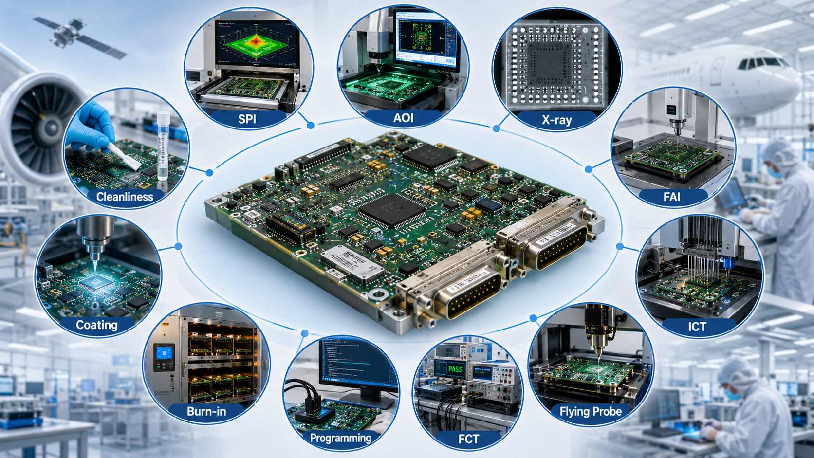
Step 13: Assembly and Lighting Test
If PCBA service is included, UV LEDs and related parts are assembled by SMT. After reflow, the board should go through AOI, polarity check, lighting test, and thermal run test. A 4–24 hour lighting test helps confirm brightness and heat dissipation.
How to Choose a Reliable China Metal-Core PCB Fabrication Manufacturer for Insect Traps?
A reliable China metal-core PCB fabrication manufacturer should provide material transparency, engineering review, controlled production, testing, and export support. For insect trap projects, the supplier should understand UV LED heat, white solder mask stability, insulation safety, and batch consistency.
Selection points:
- Material confirmation: Aluminum grade, dielectric conductivity, dielectric thickness, copper thickness, and breakdown voltage should be clear.
- Thermal review: The factory should check LED density, copper area, mounting holes, and housing contact.
- Surface finish support: ENIG, lead-free HASL, OSP, or immersion silver should be selected by pad size and storage time.
- White solder mask control: Ink adhesion, UV resistance, reflectivity, and discoloration risk should be checked.
- Testing capability: E-test, visual inspection, dimensional inspection, hi-pot test, and thermal run test should be available.
- Prototype and mass production: The supplier should support sample review, pilot run, and stable batch production.
- Assembly service: SMT, AOI, reflow control, polarity check, and lighting test are useful for turnkey projects.
- Export packaging: White solder mask, ENIG pads, and aluminum edges should be protected during shipping.
FAQs About Metal-Core PCB Fabrication for LED Insect Light Traps
Q1: What MCPCB stackup is commonly used for LED insect light traps?
A1: Most LED insect light trap MCPCBs use a single-sided aluminum-core structure: copper circuit layer, thermal dielectric, and aluminum base. Common specifications include 1 oz–2 oz copper, 1.0–3.0 W/m·K dielectric, and 1.0–2.0 mm aluminum thickness.
Q2: Can the same MCPCB support both UV LEDs and driver components?
A2: Yes, if the circuit is simple and heat distribution is controlled. Many insect trap boards place UV LEDs, resistors, connectors, and basic driver parts on the same MCPCB. For complex driver circuits or heat-sensitive components, separating the LED board and control PCB is safer.
Q3: What LED pad design improves soldering quality on MCPCB?
A3: LED pads should match the UV LED package datasheet and leave stable solder mask clearance. For many SMT UV LEDs, pad clearance is commonly 0.10–0.20 mm. Pads should stay flat, clean, and free from oxidation to reduce LED tilt and solder defects.
Q4: What causes early UV LED failure on insect trap MCPCBs?
A4: Common causes include poor heat dissipation, excessive LED current, weak solder joints, uneven LED temperature, low-grade solder mask, and poor contact between MCPCB and housing. Prototype review should check LED current, board temperature, solder quality, mounting pressure, and thermal interface contact.
Q5: Should LED insect trap MCPCBs use constant-current design?
A5: Constant-current control is recommended for stable UV LED output. UV LEDs are sensitive to current and temperature changes. Excess current raises junction temperature and speeds up LED decay. Stable current helps maintain brightness, wavelength, and product performance during long operation.
Q6: What working temperature should be controlled on the LED MCPCB?
A6: A practical target is to keep the LED board surface below 70°C after thermal balance. The exact limit depends on LED datasheet, enclosure design, and ambient temperature. Temperature should be measured after continuous operation, not only in the first few minutes.
Q7: Is ENIG always necessary for LED insect trap MCPCB fabrication?
A7: ENIG is not always required, but it is recommended for higher-quality UV LED boards, export projects, and long storage. Typical ENIG thickness is 3–6 µm nickel and 0.05–0.10 µm gold. It provides flat pads and better oxidation resistance.
Q8: How does board thickness affect insect trap MCPCB performance?
A8: Board thickness affects stiffness, heat spreading, and housing fit. Common aluminum MCPCB thickness is 1.0 mm, 1.5 mm, or 2.0 mm. Thin boards reduce weight, while thicker boards improve mechanical strength and flatness.
Q9: What should be checked before SMT assembly of UV LEDs?
A9: Check LED pad cleanliness, surface finish, solder mask alignment, board warpage, LED polarity, BOM accuracy, and stencil opening. For UV LED arrays, AOI inspection and polarity confirmation should be completed before functional testing.
Q10: Can LED insect trap MCPCBs be customized into round or long strip shapes?
A10: Yes. LED insect trap MCPCBs can be made as round boards, long strips, ring boards, rectangular modules, or housing-matched shapes. Long boards require better warpage control, while round boards require accurate routing and mounting hole placement.
Q11: What information is required for a metal-core PCB fabrication quote?
A11: A complete quote should include Gerber files, drill files, board thickness, copper thickness, base material, thermal conductivity, surface finish, solder mask color, quantity, and testing requirements. For LED trap projects, LED power, working voltage, board size, and assembly files are also useful.
Q12: How can buyers reduce MCPCB cost without increasing failure risk?
A12: Buyers can use aluminum instead of copper, select 1 oz–2 oz copper based on current, avoid unnecessary high-conductivity dielectric, and standardize board thickness. Cost should not be reduced by using poor solder mask, unstable surface finish, or skipping electrical testing.
Q13: What tests are useful before mass production of insect trap MCPCBs?
A13: Useful checks include 100% E-test, hi-pot test when required, solderability check, appearance inspection, dimension inspection, LED lighting test, and thermal run test. For outdoor or humid applications, humidity and thermal cycling tests can also be added.
Q14: What defects should buyers check after receiving MCPCBs?
A14: Buyers should check scratches, stains, oxidized pads, solder mask pinholes, yellowing, board warpage, aluminum burrs, hole defects, and poor surface finish. For LED trap boards, LED pad flatness and housing fit should also be checked.
Q15: Can a China metal-core PCB fabrication manufacturer support prototype and mass production for insect traps?
A15: Yes. A qualified China MCPCB manufacturer can support prototype fabrication, engineering review, small-batch testing, and mass production. For insect trap projects, the factory should confirm thermal material, LED pad quality, white solder mask stability, inspection method, packaging protection, and global delivery requirements.
Conclusion
Metal-core PCB fabrication for LED insect light traps should focus on heat transfer, UV LED stability, insulation safety, and production consistency. Aluminum core suits most standard insect trap boards, while copper core is better for compact high-power modules. Buyers should confirm copper thickness, dielectric thermal conductivity, surface finish, white solder mask quality, and board thickness before production.
EBest Circuit is a China source factory and global supply manufacturer for custom metal-core PCB fabrication, prototype review, batch production, and assembly support. We can support LED insect trap PCB projects from material selection to finished PCBA delivery. Send your Gerber files, BOM, drawings, and technical requirements to sales@bestpcbs.com for a fast quotation.