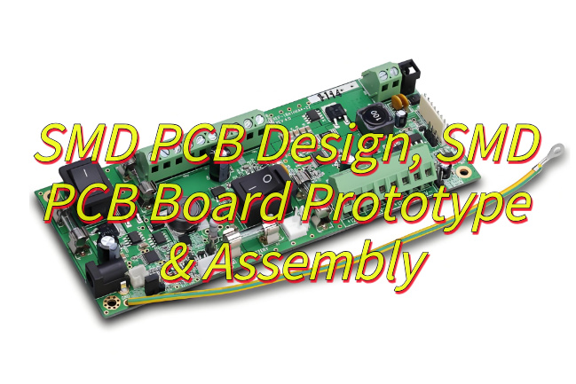
Ever wondered how mastering SMD PCB design can optimize your surface-mount technology projects? This guide explores essential software tools, design methodologies, prototyping techniques, and assembly quality controls for reliable SMD PCB production.
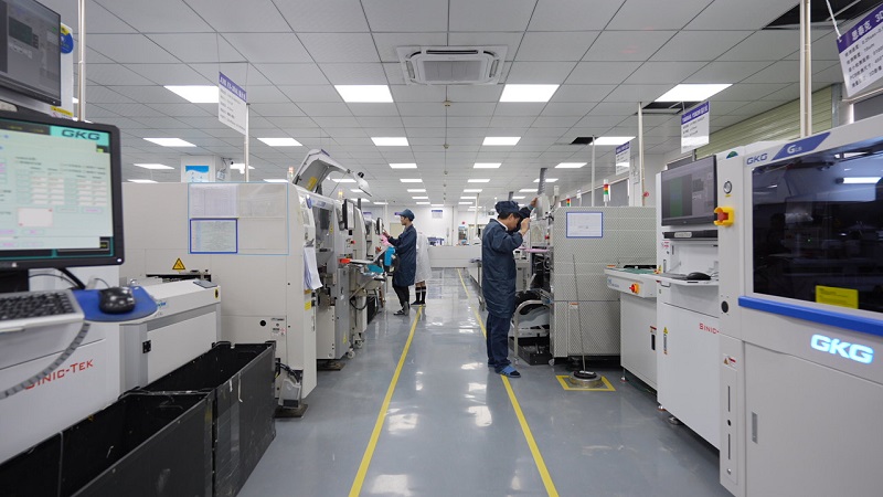
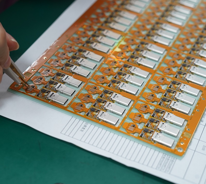
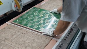
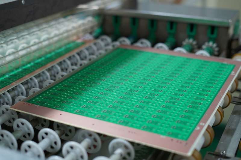
EBest Circuit (Best Technology) stands as your trusted partner for end-to-end SMD PCB solutions – from precision SMD PCB design to PCBA service. Our complete one-stop service eliminates multiple vendor coordination hassles, while our stable electronic supply chain ensures uninterrupted material flow for your projects. We specialize in ultra-fast 24-hour prototyping with industry-leading 0.2mm placement accuracy, dramatically reducing your time-to-market. Our engineering team combines 15+ years of SMD expertise with advanced DFM analysis to prevent assembly failures and optimize your board performance. We maintain strict IPC Class 2/3 standards across our automated SMT lines, supported by AOI and X-ray inspection for flawless quality control. Whether you need LED arrays, high-density designs, or complex multilayer boards, we deliver cost-effective solutions with responsive 24/7 customer support. Partner with us to transform your concepts into reliable PCBs with fastest turnaround in the industry – request your quote today: sales@bestpcbs.com.
What Is SMD PCB Design?
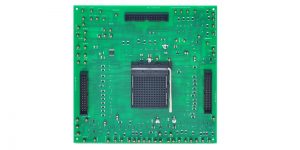
SMD PCB design refers to the process of creating printed circuit boards specifically optimized for surface mount devices, where components are mounted directly onto the board’s surface rather than through holes. It involves precise layout planning to accommodate miniature components like resistors, capacitors, and ICs with tight spacing requirements, while ensuring proper pad sizing, solder mask openings, and thermal management for reflow soldering. The SMD PCB design must account for high-density interconnects, signal integrity in high-frequency circuits, and manufacturability constraints such as pick-and-place machine tolerances. Effective SMD PCB design balances component placement efficiency, electrical performance, and assembly feasibility to achieve reliable mass production.
What Software Simplifies SMD PCB Design?
Below are selection tips of SMD PCB design software:
Altium Designer
- Combines schematic capture, PCB layout, and 3D visualization in one platform.
- Includes tools for auto-routing dense SMD designs, real-time component availability checks, and solder paste analysis.
- Validates thermal performance and signal integrity during operation.
EAGLE (Autodesk)
- User-friendly interface with modular design blocks and hierarchical schematics.
- Offers 3D component models for SMD packages and clearances checks.
- Works with Autodesk Fusion 360 for mechanical design collaboration.
KiCad
- Free, cross-platform software with footprint creation tools.
- Features interactive routing and 3D board inspection.
- Exports BOMs with supplier links for easy sourcing.
OrCAD
- Ideal for high-speed and RF designs with constraint-driven tools.
- Manages impedance control and length matching for SMD traces.
- Uses Allegro PCB Editor for advanced HDI layouts.
Proteus Design Suite
- Links PCB design with embedded system simulation.
- Includes JEDEC-compliant SMD libraries and auto-alignment features.
- Exports 3D models for enclosure testing.
EasyEDA
- Cloud-based collaboration with real-time editing.
- Prepares files for low-cost assembly services.
DipTrace
- Customizable SMD land patterns and 3D preview.
- Autorouter handles fine-pitch components and escape routing.
- Imports DXF files for mechanical design alignment.
Upverter
- Web-based tool with GitHub-style version control.
- Searches SMD components by footprint dimensions.
- Generates assembly-ready files with placement coordinates.
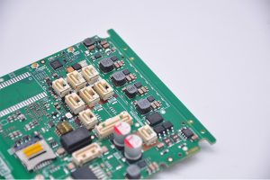
How Do SMD PCB Design Rules Prevent Assembly Failures?
Here are rules about SMD PCB design prevent assembly failures:
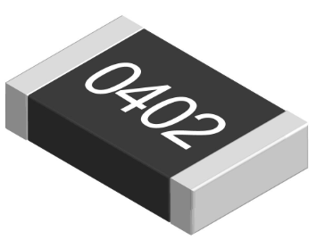
- Component Spacing and Clearance – Design rules enforce minimum spacing between SMD components to prevent solder bridging and enable precise pick-and-place machine operation. Adhering to clearances (e.g., 0.1mm for 0402 parts) reduces rework and ensures compatibility with automated optical inspection (AOI).
- Solder Paste Stencil Alignment – Rules define stencil aperture sizes and offsets relative to SMD pads to prevent solder paste skewing during stencil printing. Proper alignment ensures consistent solder joints for fine-pitch components like QFNs and BGAs.
- Pad Geometry and Copper Balance – Design rules specify pad shapes (e.g., rectangular for 0603 resistors, thermal pads for QFNs) and copper balance around pads. Symmetrical pad designs minimize tombstoning during reflow, while thermal pads prevent voiding in ground-plane-connected components.
- Via Placement Restrictions – Rules prohibit vias under SMD pads to avoid solder wicking and void formation. Blind/buried vias are restricted to inner layers to ensure proper solder flow and joint reliability for components like 0201 capacitors.
- Trace Exit Angles from Pads – Design rules mandate 45° trace exits from SMD pads to reduce solder paste slump and improve reflow quality. Sharp angles are prohibited to prevent solder balling in high-density areas.
- Component Orientation Guidelines – Rules enforce consistent orientation for asymmetric components using polarity markers (e.g., diode lines, IC notches). Clear orientation standards simplify automated assembly and reduce placement errors.
- Panelization and Fiducial Markers – Design rules require fiducial markers (3-5 per panel) for machine vision alignment during assembly. Panelization rules define scoring/routing parameters to minimize stress on SMD components during depanelization.
- Silkscreen and Assembly Layer Rules – Rules govern silkscreen legibility (0.15mm minimum line width) and placement outside solder mask openings. Clear polarity markers and reference designators reduce assembly errors and rework.
- Thermal Relief for High-Power Components – Design rules implement thermal spokes (4-8 connections) for power SMD components to balance heat dissipation and solderability. Proper relief prevents tombstoning and ensures consistent reflow profiles.
- Design for Test (DFT) Rules – Rules incorporate test points (0.8mm minimum diameter) for in-circuit testing of SMD nodes. Accessible test pads enable automated test equipment (ATE) probing without damaging components.
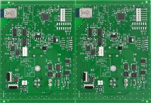
How to Design A SMD PCB?
Below are SMD PCB design processes:
1.Define Project Requirements
- Outline electrical specifications, operational environment (temperature range, vibration tolerance, humidity exposure), mechanical constraints (board dimensions, mounting hole locations), and regulatory standards (RoHS compliance, UL certification). Detail signal types (analog, digital, RF), power distribution requirements, and thermal management priorities to establish design boundaries.
2.Schematic Capture
- Develop a precise circuit diagram using EDA tools such as KiCad or Altium. Organize components by functional blocks (power supply, microcontroller, sensor interfaces) and label all nets with clear designators. Validate connectivity through electrical rule checks (ERC) to resolve errors early.
3.Component Selection
- Choose SMD packages aligned with assembly capabilities (e.g., 0402 for compact signals, QFN for high-density layouts). Prioritize components with verified footprints in PCB libraries and multiple supplier options to reduce supply chain risks.
4.PCB Stack-up Planning
- Determine layer configuration (2-layer for basic designs, 4+ layers for complex routing). Select dielectric materials (FR4 for cost efficiency, specialized laminates for RF applications). Define copper weights (1oz for power planes, 0.5oz for signal traces) and incorporate ground/power planes to minimize electromagnetic interference.
5.Placement Strategy
- Position high-power components near connectors and place decoupling capacitors within 1mm of IC power pins. Orient RF components perpendicular to digital circuitry and reserve clearance for mechanical fixtures. Group related circuits to shorten trace lengths and enhance signal integrity.
6.Routing Guidelines
- Route differential pairs with length matching (±2mm tolerance) and maintain 3W spacing (trace gap ≥3x width) for high-voltage traces. Use 45° bends to reduce reflections and avoid routing under crystal oscillators. Isolate analog and digital grounds using a single-point star connection.
7.Thermal Management
- Integrate thermal vias beneath heat-generating components (SOIC, QFP) and utilize copper pours with stitching vias for heat dissipation. Conduct thermal simulations for designs exceeding 85°C and align component placement with enclosure airflow paths.
8.Design for Manufacturing (DFM)
- Apply 0.1mm minimum trace/space for standard fabrication and include fiducial markers for assembly alignment. Add tooling holes for panelization and ensure silkscreen legibility (0.15mm line width). Avoid placing SMD pads near board edges to prevent damage during handling.
9.Signal Integrity Measures
- Add termination resistors for high-speed signals (>50MHz) and control impedance traces (50Ω for RF, 90Ω for differential pairs). Use guard traces around sensitive analog inputs and isolate switching regulators from noise-sensitive circuits.
10.Documentation & Validation
- Generate a comprehensive BOM with manufacturer part numbers and alternative sources. Create assembly drawings detailing polarity markers and component orientation. Execute design rule checks (DRC) for clearances and short circuits. Share Gerber files in 274X format with fabricators for production.
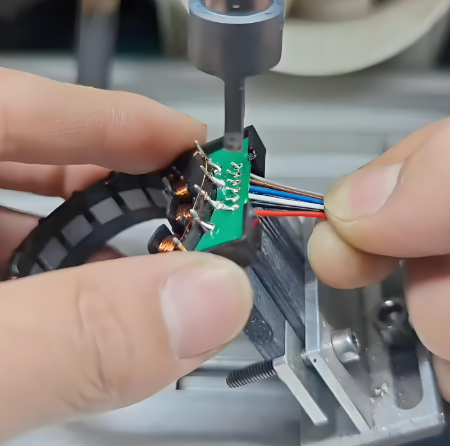
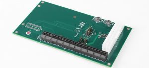
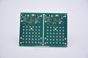
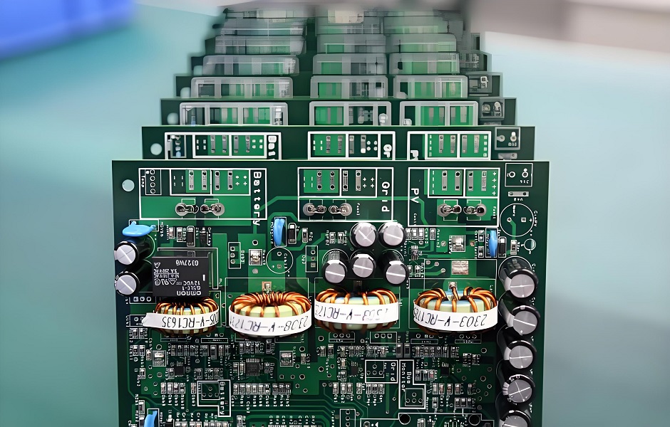
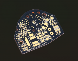
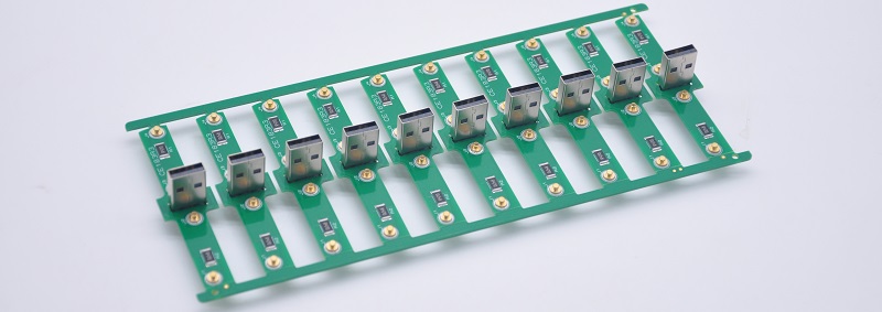
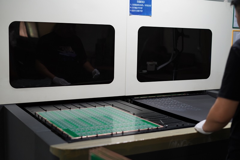
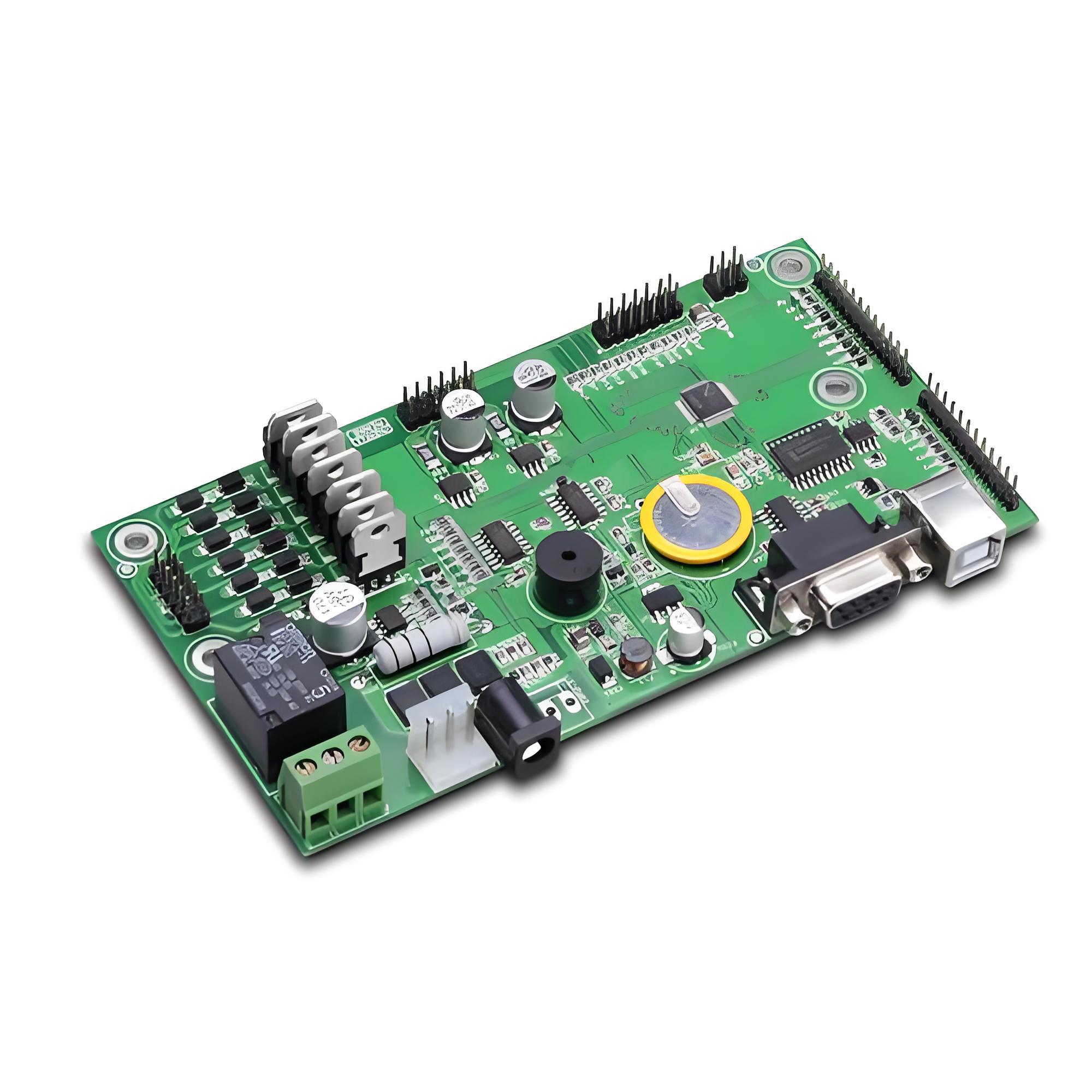
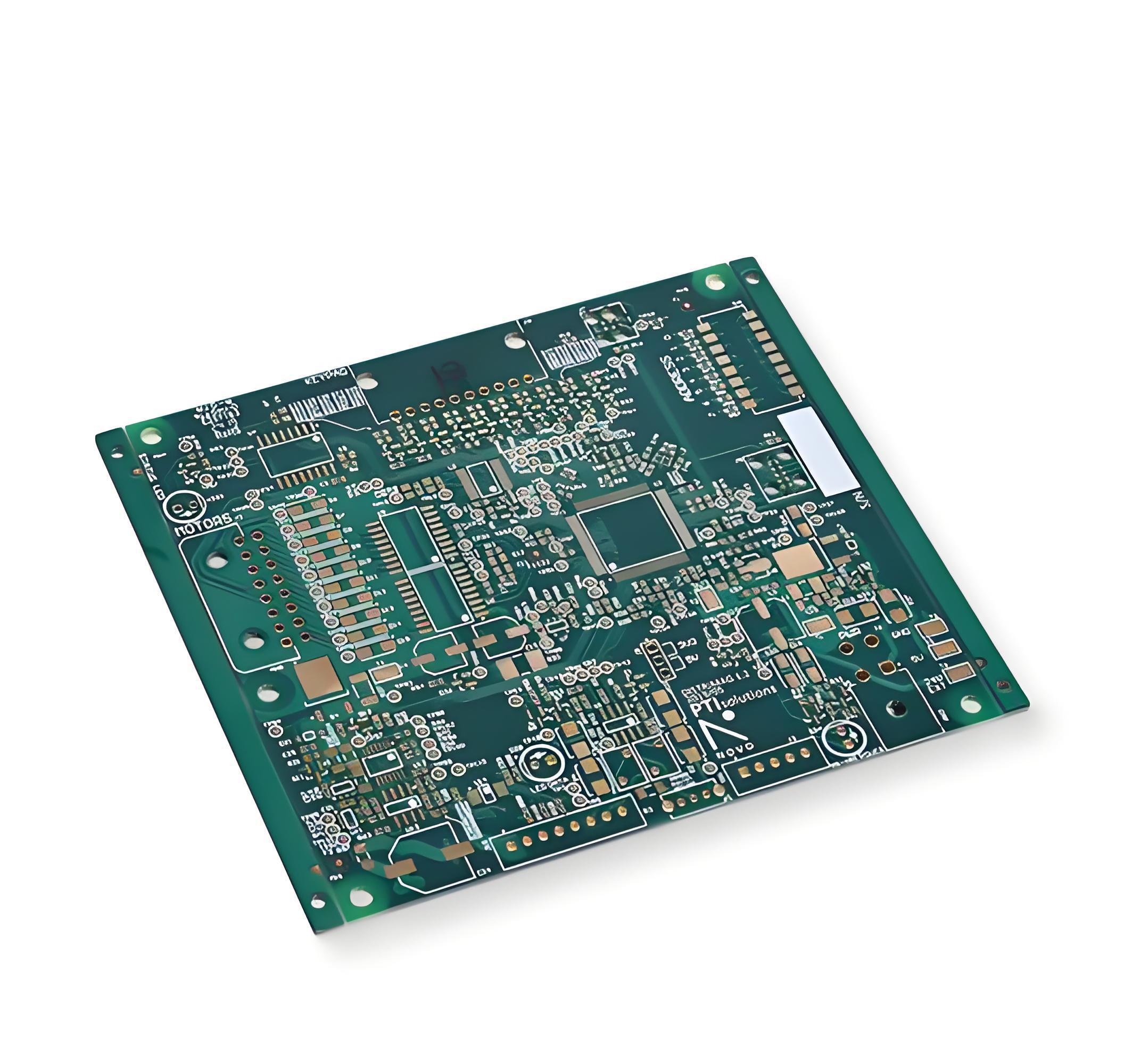
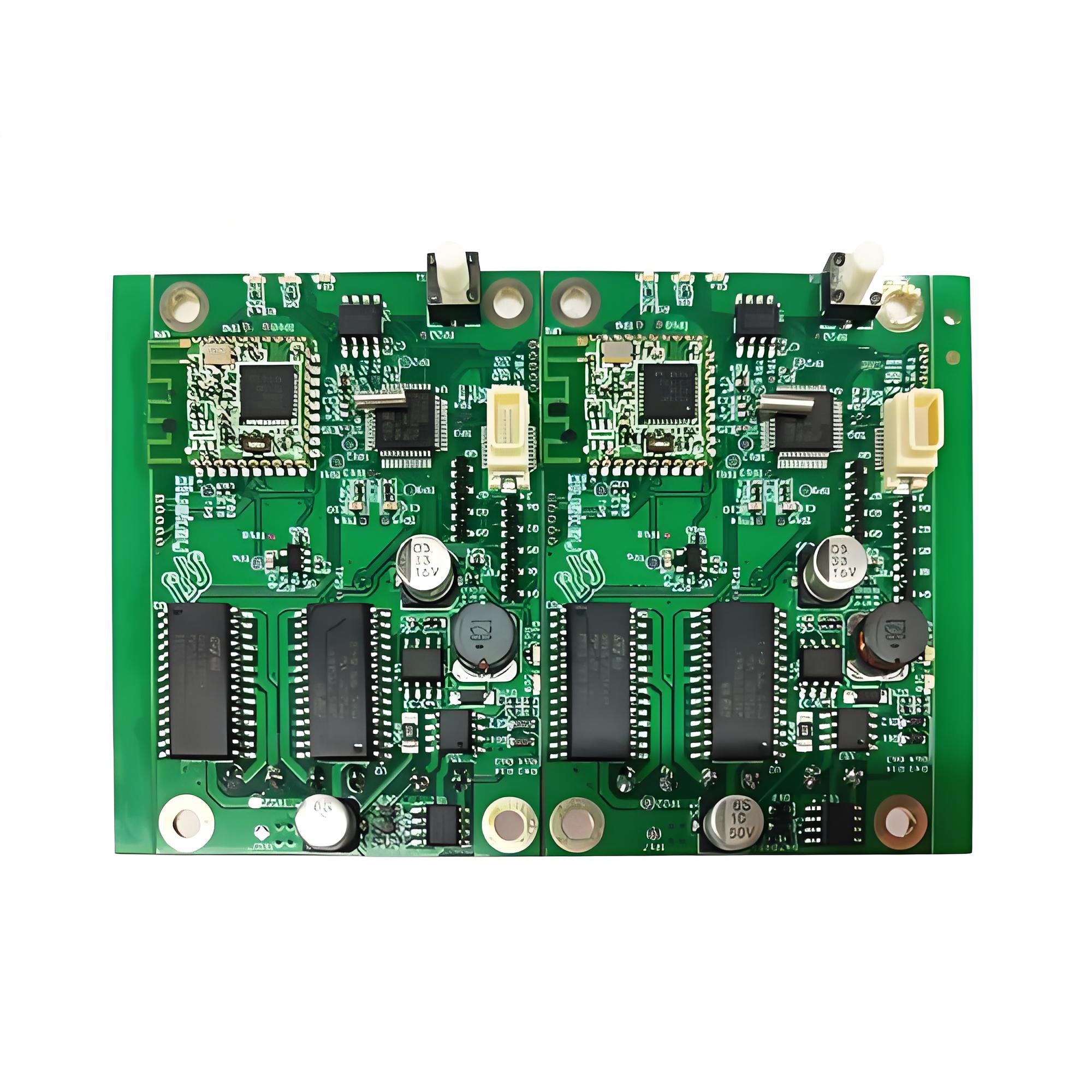
What Is SMD PCB Board Prototype?
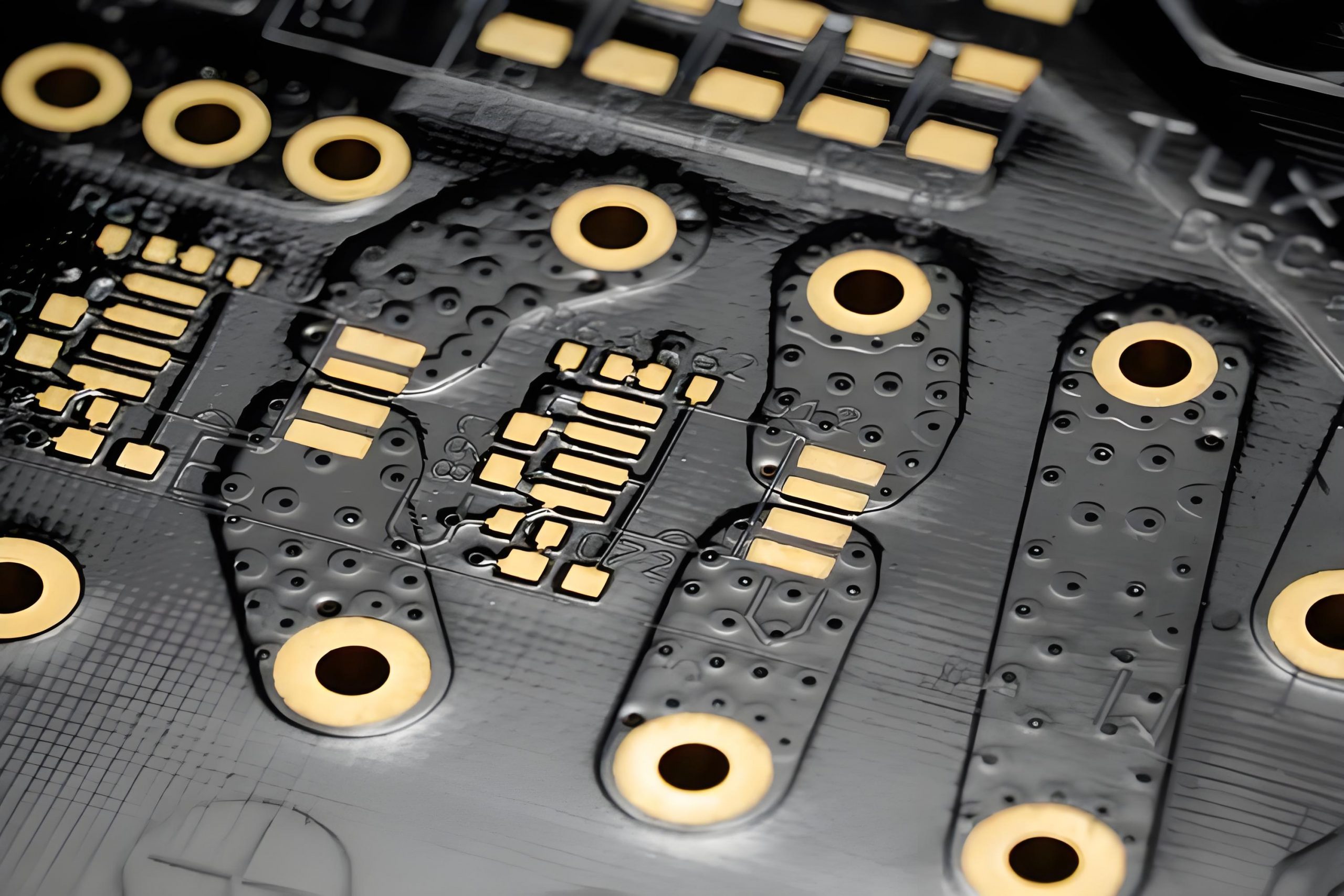
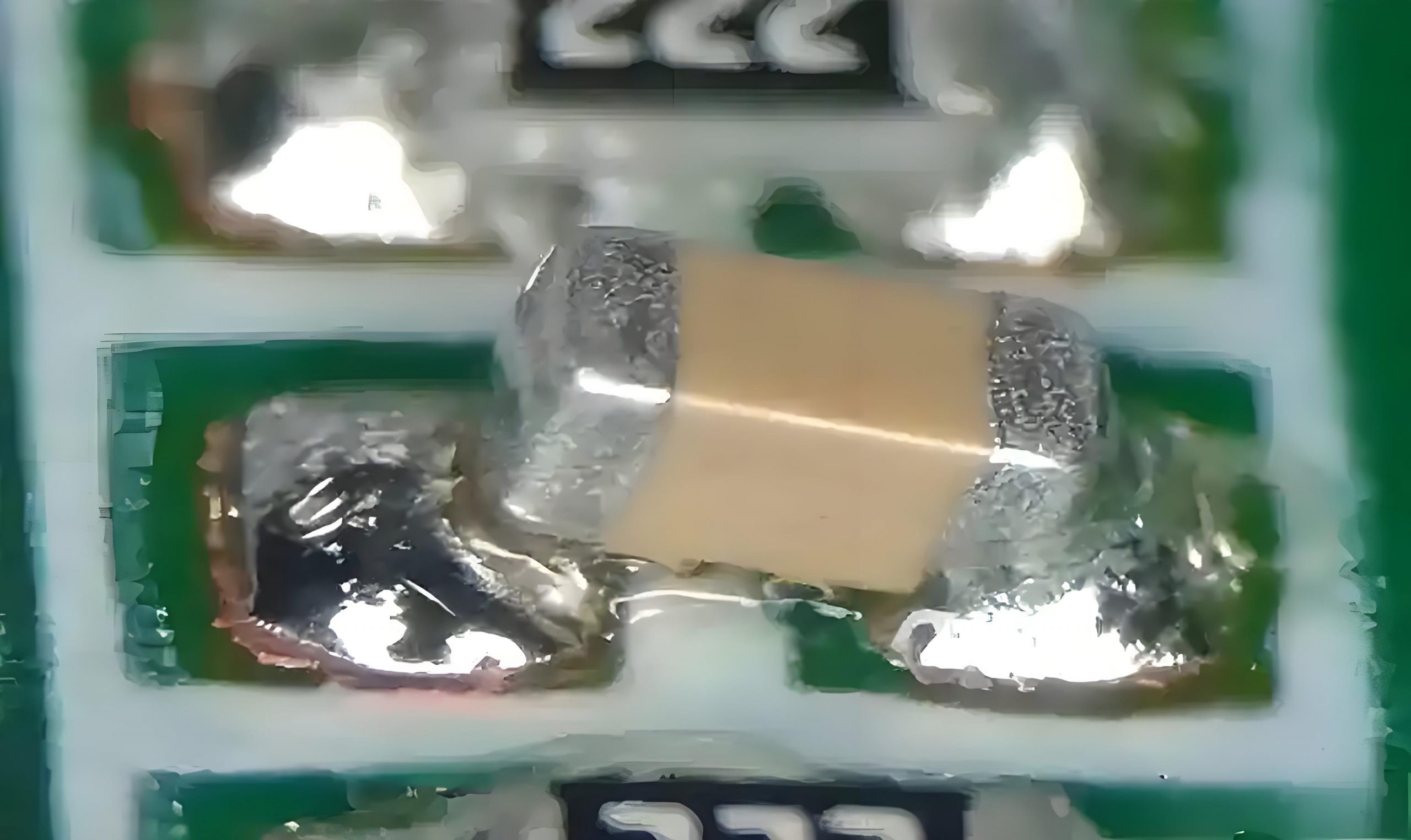
A SMD PCB board prototype is a functional test version of a printed circuit board designed for surface mount technology, featuring components soldered directly onto copper pads without through-hole connections. It validates the SMD PCB design’s feasibility by testing component placement accuracy, solder joint reliability, and electrical performance under real-world conditions before mass production. The prototype typically undergoes design iterations to refine pad geometries, solder mask clearances, and trace routing for optimal SMD assembly yield and signal integrity.
How to Achieve SMD PCB Board Rapid Prototyping?
Design Optimization for Speed
- Use standardized component libraries (e.g., 0402 resistors, SOT-23 transistors) to reduce part sourcing delays.
- Simplify board geometry to rectangular/square shapes for efficient panelization and lower fabrication costs.
- Apply design rule checks (DRC) early to eliminate errors that delay manufacturing.
Leverage Rapid Prototyping Software
- Adopt EDA tools with real-time DFM feedback (e.g., Altium 365, Upverter) to identify issues during layout.
- Use parametric footprint generators for custom SMD packages to avoid manual errors.
- Export Gerber/ODB++ files directly to fabricators without intermediate steps.
Material and Process Selection
- Choose FR4 laminates with 1.6mm thickness for cost efficiency and mechanical robustness.
- Prioritize ENIG (Electroless Nickel Immersion Gold) surface finish for solderability and long shelf life.
- Specify solder mask colors (e.g., green) with high contrast for silkscreen readability.
On-Demand Manufacturing Partnerships
- Utilize quick-turn PCB fabricators (e.g., JLCPCB, PCBWay) offering 24-hour turnaround for 2-layer boards.
- Select assembly services with SMT lines supporting 0201 components and BGA rework capabilities.
- Prioritize vendors offering BOM optimization tools to suggest drop-in replacements for out-of-stock parts.
Automated Assembly Strategies
- Submit centroid files and pick-and-place coordinates for automated SMD placement.
- Use stencil kits with pre-cut foil for solder paste application to reduce setup time.
- Request selective soldering for through-hole components if mixed technology is required.
Parallel Testing and Validation
- Design test jigs with pogo pins for bed-of-nails fixture testing to accelerate functional verification.
- Use flying probe testers for impedance measurements without dedicated test coupons.
- Implement boundary-scan (JTAG) testing for complex SMD assemblies to reduce debug time.
Iterative Refinement Workflow
- Adopt agile design practices with 2-3 revision cycles per prototype iteration.
- Use 3D PCB viewers to detect component clearance issues before fabrication.
- Document assembly feedback (e.g., solder joint quality, part orientation) for continuous improvement.
Cloud-Based Collaboration Tools
- Share design files via platforms like Google Drive or Autodesk Fusion Team for real-time feedback.
- Use version control systems (e.g., KiCad’s built-in tools) to track design changes.
- Host video conferences with fabricators during DFM reviews to resolve issues instantly.
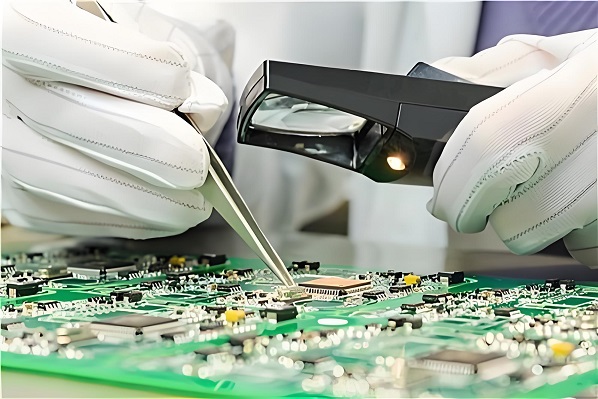
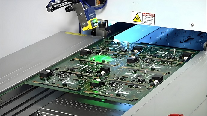
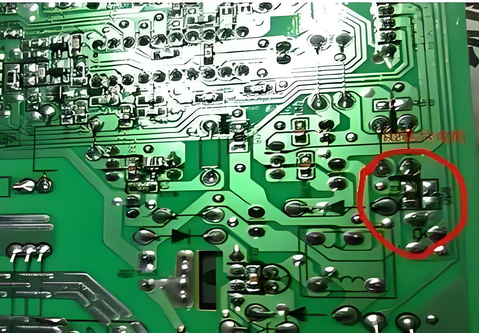
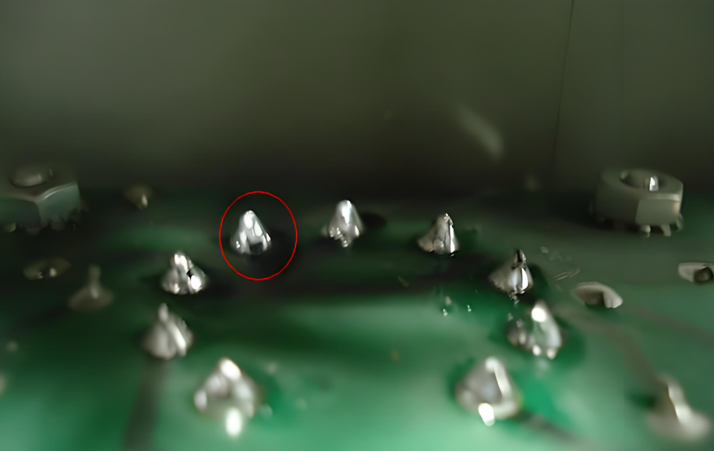
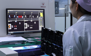
How to Detect Placement Offset Issues During SMD PCB Assembly?
This is how to detect placement offset issues during SMD PCB assembly:
- Use AOI Systems with Machine Learning: Set up automated optical inspection (AOI) tools using multi-angle cameras and AI. Train them to spot misaligned parts by setting tolerance limits (like ±0.05mm for tiny components). Add polarized lighting to highlight bad solder joints or rotated parts.
- Check Hidden Packages with X-Rays: For BGA or QFN chips, use 2D/3D X-ray machines to see solder joints and alignment under the package. Look for uneven ball spacing or voids that signal placement issues.
- Run In-Circuit Tests (ICT) with Boundary Scan: Test electrical connections with ICT probes or JTAG. This catches functional failures from components that aren’t properly seated or connected.
- Build Functional Test Jigs: Create jigs with spring-loaded pins to press onto SMD pads during power tests. Watch for odd voltage/current readings that hint at misaligned parts disrupting circuits.
- Add Test Points for Easy Checking: Include extra pads near dense SMD areas for manual or automated microscope checks. Use fiducial markers as guides during visual inspections.
- Track Placement Data with SPC: Collect info from pick-and-place machines to spot offset trends. Use charts to catch machine drift before defects happen.
- Slice Boards for Cross-Section Analysis: Cut prototype boards to check solder joints and alignment under a microscope. Compare results to IPC-A-610 standards.
- Spot Heat Issues with Thermal Cameras: Use infrared cams to find uneven heating from misaligned power parts. Hotspots mean bad thermal contact due to placement errors.
- Train Staff with AR Tools: Teach operators to spot offset patterns (like skewed ICs) using AR overlays. Use checklists to avoid mistakes during manual checks.
- Work with Suppliers to Fix Root Causes: Share placement data with assembly partners to link offsets to stencil printing or machine settings. Use 8D problem-solving to tackle issues like worn nozzles.
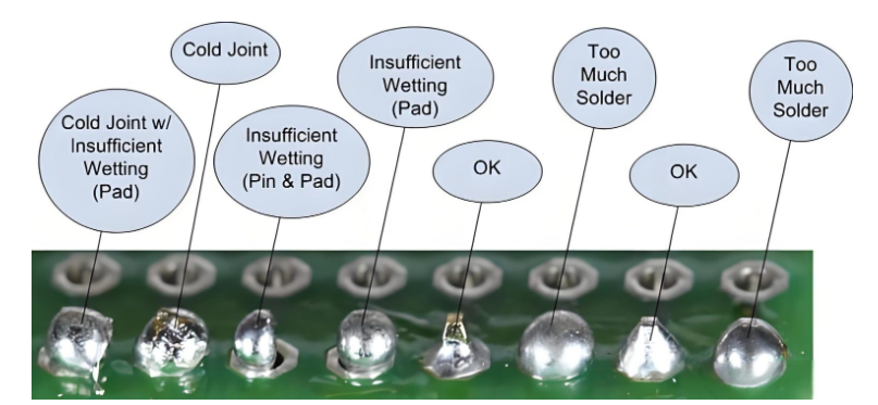
How to Ensure Consistent Solder Paste Thickness in Batch SMD PCB Assembly?
Here are tips about how to ensure consistent solder paste thickness in batch SMD PCB assembly:
- Use Precision Stencils – Choose laser-cut stainless-steel stencils with thicknesses matched to your components (e.g., 0.1mm for small resistors). Stepped stencils help manage varying paste needs across the board.
- Adjust Printing Settings – Set squeegee speed (20–80mm/s) and pressure (3–5kg/cm²) based on your solder paste’s viscosity. Maintain a small gap (0.5–1.0mm) between the stencil and PCB to avoid smears.
- Pick the Right Solder Paste – Use Type III/IV pastes with an 8–12-hour working life. Store paste properly (2–10°C) and let it warm up before use to keep consistency.
- Monitor with 3D Inspection – Deploy SPI systems to check paste volume, area, and height after printing. Set tolerance limits (e.g., ±20% volume) and link data to your machines for real-time adjustments.
- Control the Environment – Keep the printing area at 23±2°C and 45–65% humidity. Use sealed storage for stencils to prevent oxidation between batches.
- Check First Prints Carefully – Examine early prints under a microscope or using microsectioning. Compare results to standards like IPC-7525 to set your baseline.
- Clean Stencils Regularly – Clean stencils every 10–20 prints with alcohol and soft wipes. Replace stencils after 5,000–10,000 prints or when wear exceeds 5µm.
- Train Staff to Spot Issues – Teach teams to recognize common problems like bridging or uneven paste using visual guides. Review SPC charts daily to catch trends early.
- Automate Stencil Cleaning – Use ultrasonic or vacuum cleaners for thorough, damage-free stencil cleaning. Set consistent scan rates (5–10µm/second) for reliable results.
- Keep Detailed Records – Track every batch’s paste, stencil, and inspection data. Audit processes monthly to ensure standards are met.
Conclusion
In conclusion, that’s all about software tools selection tips, design methodologies for SMD PCB design, prototyping techniques and assembly quality controls for SMD PCB board. If you want to know more about SMD PCB design, prototype and assembly, please feel free to contact us: sales@bestpcbs.com.