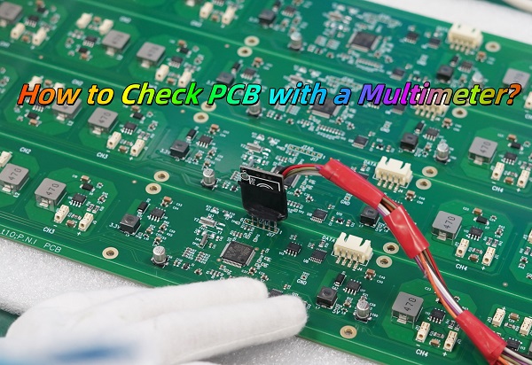
When communicate with clients, they always ask why the PCB board are so expensive? Is there any basis for that? Actually, the price of PCBs are made specifically according to its manufacturing process, layers, complexities and so on. Today, EBest Circuit (Best Technology) is deeply sharing the composition of PCB cost. Welcome to keep reading.
Why is PCB Board So Expensive?
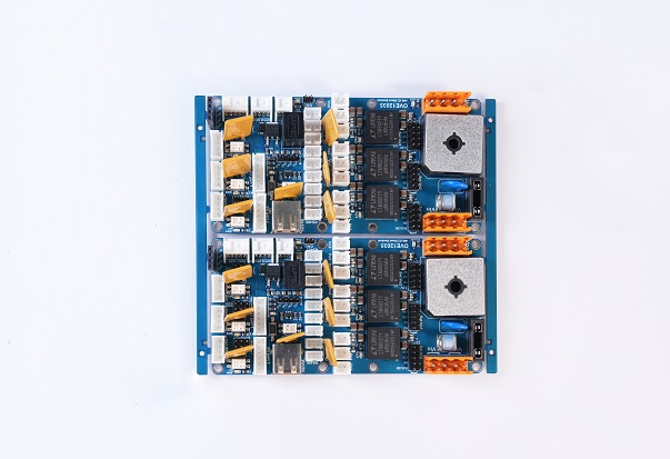
The cost of a PCB can sometimes seem high due to several reasons. Firstly, the complexity of the design plays a significant role. High-density interconnect (HDI) PCBs, multi-layer PCBs, and those requiring advanced materials or special finishes can drive up the cost. Additionally, stringent quality control measures and the need for precise manufacturing processes add to the expense.
Another factor is the cost of raw materials. Copper, laminates, and specialty substrates can vary in price, affecting the overall cost of the PCB. Furthermore, labor costs in the region where the PCB is manufactured, along with overhead costs such as utilities and facility maintenance, contribute to the final price.
What Factors Affect the PCB Board Cost?
PCB board can cost from $10 to $500 to produce. Buyers are always amazing that why PCB cost so high? But they don’t know there are numerous factors a manufacturer considers in determining PCB costs. If you are in the market to design a PCB, this guide provides factors to consider that could increase or decrease the cost of circuit boards.
- Manufacture technology
The specific technology used in the PCB can significantly impact the cost. Advanced technologies such as HDI (High-Density Interconnect), embedded busbar or flexible PCBs often require more complex manufacturing processes, which can increase the cost.
- Material Type
The type of materials used for the PCB, such as standard FR4, high-frequency laminates, or other specialty substrates, can influence the cost. Higher quality or specialized materials typically cost more.
- IPC Grade
The IPC standards and grades indicate the quality and reliability requirements of the PCB. In electronics manufacturing, printed circuit boards are divided into three levels: level 1, level 2 and level 3. These grades reflect the quality level of each board type, from the lowest (Level 1 standard) to the highest (Level 3 standard). This classification system was developed and defined by IPC and is specified in the IPC-6011 series.
- Circuit Design
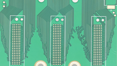
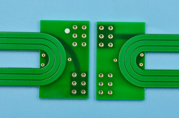
The complexity of the circuit design, including the number of layers, trace width, and spacing, affects the cost. More intricate designs require more precision and advanced techniques, leading to increased expenses.
- PCB Size & Yield
The physical dimensions of the PCB and the yield rate during production play a role in the overall cost. Larger boards or designs with lower yield rates (more defects) will typically cost more to produce.
- Material Thickness
The thickness of the materials used in the PCB construction, such as the substrate and copper layers, can impact the cost. Thicker materials may be more expensive and require more resources to process.
- Copper Thickness
The thickness of the copper used in the PCB, measured in ounces per square foot, can affect the cost. Thicker copper layers provide better electrical performance but are more expensive.
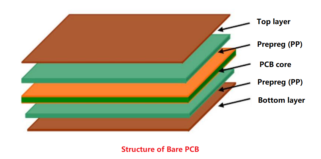
- Stack-up
The method of layering and stacking the materials in the PCB, known as the stack-up configuration, can influence the cost. Complex stack-ups with multiple layers and specific arrangements can be more costly to manufacture. Read our another post of How Can I Reduce and Optimize the Cost of My PCB in A Best Way?
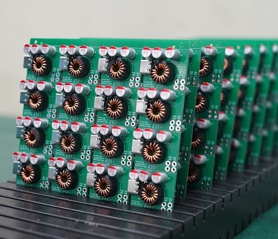
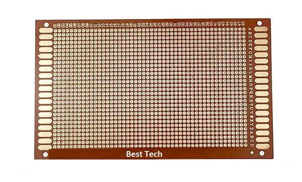
Manufacturing Process of A Standard PCB
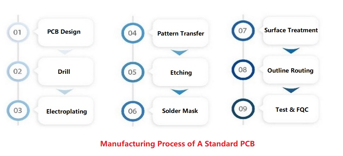
PCB Design and Layout
The manufacturing process begins with the design phase, where engineers use CAD (Computer-Aided Design) software to create the PCB layout. This includes defining the circuit paths, components, and layers, ensuring the design meets the electrical and mechanical requirements.
Once the design is finalized, a photomask is created, which is a transparent film with the PCB design printed on it. The PCB substrate, typically made of FR4, is then coated with a light-sensitive material called photoresist.
Drilling
Precise holes are drilled into the board for through-hole components and vias using computer-controlled drilling machines. The board is cleaned and deburred to remove any rough edges or debris from the drilling process.
Plating and Copper Deposition
A thin layer of copper is deposited on the surface of the board and inside the drilled holes through an electroless plating process, providing a conductive base. Additional copper is electroplated onto the board, building up the thickness of the copper traces and plated through-holes.
Pattern Transfer
The photomask is placed over the photoresist-coated substrate and exposed to ultraviolet (UV) light. The UV light hardens the photoresist where the design allows light to pass through, and the board is then developed to wash away the unhardened photoresist, leaving behind the desired circuit pattern.
Etching
The PCB undergoes an etching process using a chemical solution to remove unwanted copper, leaving only the copper traces that form the circuits. The remaining hardened photoresist is then stripped away to reveal the clean copper pattern.
Applying Solder Mask
A layer of solder mask is applied to the board to protect the copper traces from oxidation and prevent solder bridges during assembly. The solder mask is cured using UV light, hardening it and making it durable.
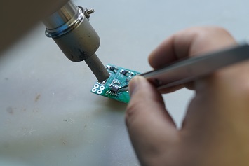
Surface Finish/Surface Treatment
A surface finish is applied to the exposed copper areas to protect them and facilitate soldering. Common finishes include HASL (Hot Air Solder Leveling), ENIG (Electroless Nickel Immersion Gold), and OSP (Organic Solderability Preservatives).
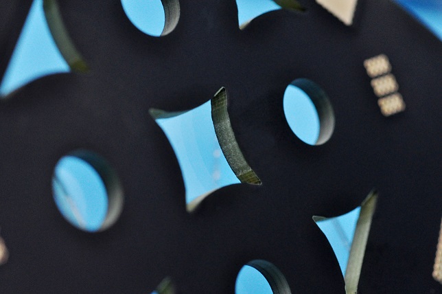
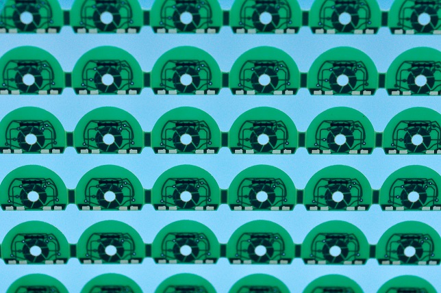
Outline Routing
One the surface treatment finish, it will be routed according to the manufacturing file by CNC machine. And then individual PCBs are cut from the larger panel using routing or V-scoring, depending on the board design and requirements.
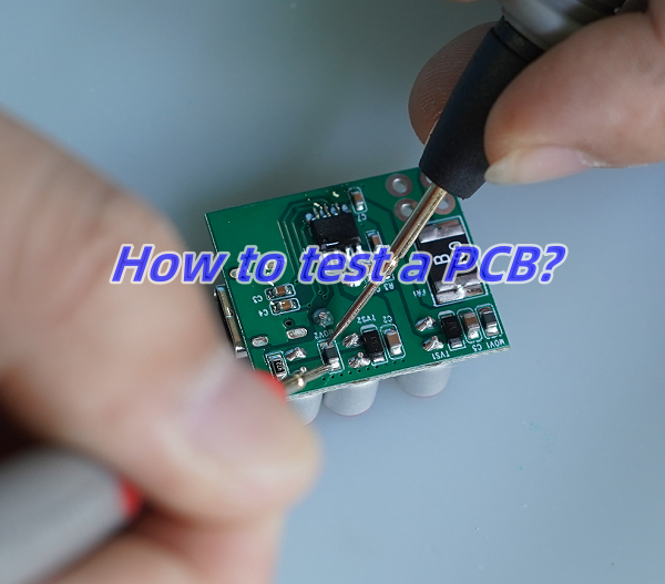
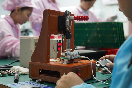
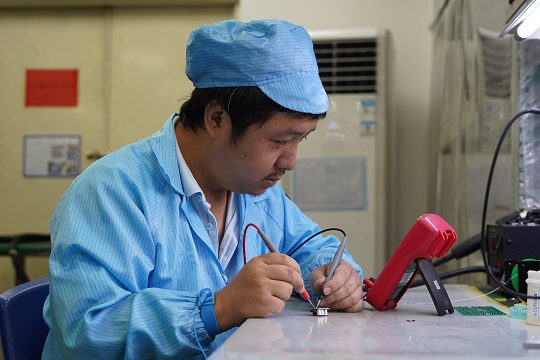
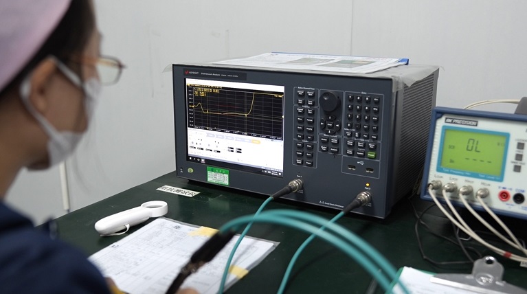
Electrical Testing & FQC
The PCB undergoes electrical testing to check for short circuits, open circuits, and other defects. This is typically done using a flying probe tester or a bed-of-nails tester. Then the board is visually inspected for any cosmetic defects or anomalies, and further tests and inspections are performed to ensure the PCB meets all specified requirements and standards. Below you can see the full manufacturing process video of a PCB:
EBest Circuit (Best Technology) – A 18+ Years Experience PCB Manufacturer
When you are looking for a reliable PCB manufacturer, considering EBest Circuit (Best Technology). We have transparent price and 5years quality warranty. We 24/7 hours online and welcome all the technical questions and PCB inquiries. Contact us for more!