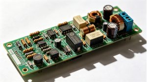
A 104 capacitor is one of the most common capacitors used in electronic circuits. The code “104” means the capacitor has a capacitance value of 100,000 pF, which equals 100 nF or 0.1 µF. You can find it in power supply filtering, IC decoupling, signal bypassing, timing circuits, sensor modules, LED drivers, automotive electronics, communication devices, and industrial control boards.
Although the value looks simple, choosing the right part is not only about capacitance. Engineers also need to check voltage rating, dielectric material, tolerance, package size, temperature stability, leakage current, ESR, safety approval, and long-term supply reliability. For buyers, the same marking may appear on ceramic, film, dipped, or safety capacitors, so the complete part number and datasheet matter more than the printed code alone.
What Is a 104 Capacitor?
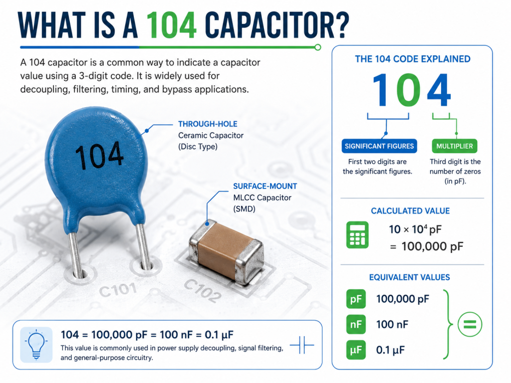
A 104 capacitor is a capacitor marked with the three-digit code “104.” This code follows a simple capacitor marking rule. The first two digits are significant numbers, and the third digit shows how many zeros should be added in picofarads.
For a 104 capacitor:
| Code | Calculation | Value |
|---|---|---|
| 104 | 10 × 104 pF | 100,000 pF |
| 104 | 100,000 pF | 100 nF |
| 104 | 100 nF | 0.1 µF |
This makes the 104 capacitor a standard 0.1 µF capacitor. It is widely used because 0.1 µF is a practical value for filtering high-frequency noise near integrated circuits, stabilizing power rails, and improving circuit reliability.
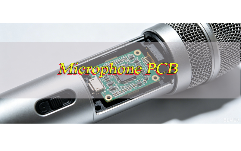
In many PCB assemblies, engineers place one 104 capacitor close to each power pin of an IC. This helps reduce voltage fluctuation caused by fast switching current.
Why Is the 104 Capacitor Important in Electronics?
The 104 capacitor is important because it provides a compact and cost-effective way to control noise, store small amounts of charge, and stabilize circuit behavior. In digital circuits, ICs switch quickly and create current spikes. A 104 capacitor placed near the IC can supply instant local current and reduce power rail disturbance.
In analog circuits, it can help smooth small voltage changes, filter unwanted frequency components, and improve signal clarity. In mixed-signal boards, it often works together with larger capacitors to build a wider filtering network.
A typical power line may use:
| Capacitor Value | Common Role |
|---|---|
| 10 µF or 22 µF | Bulk energy storage |
| 1 µF | Mid-frequency filtering |
| 0.1 µF / 104 | High-frequency decoupling |
| 10 nF or 1 nF | Very high-frequency noise control |
The 104 capacitor is small, inexpensive, and available in many packages, which makes it a default choice in both prototype and mass production designs.
How Does a 104 Capacitor Work?
A capacitor stores electrical energy between two conductive plates separated by an insulating material called dielectric. When voltage is applied, electric charge accumulates on the plates. When the circuit needs a short burst of current, the capacitor can release that stored energy quickly.
In a 104 capacitor, the capacitance value is 0.1 µF, which is suitable for fast charge and discharge behavior. This is why it is frequently used for bypass and decoupling functions.
In a PCB circuit, the working behavior depends on several factors:
| Factor | Effect on Performance |
|---|---|
| Capacitance | Defines charge storage capacity |
| Voltage rating | Defines safe operating voltage range |
| Dielectric | Affects stability, loss, and aging |
| ESR | Influences filtering and heat behavior |
| ESL | Affects high-frequency performance |
| Placement | Determines real decoupling efficiency |
For high-speed circuits, the PCB layout can be as important as the capacitor itself. A 104 capacitor placed far from the IC may lose much of its filtering effect because the trace inductance becomes too high.
What Are the Main Types of 104 Capacitors?
The marking “104” only tells the capacitance value. It does not identify the capacitor type. Different 104 capacitors may have very different materials, structures, voltage ratings, and applications.
| Type | Common Use | Key Feature |
|---|---|---|
| Ceramic 104 capacitor | IC decoupling, bypass, general circuits | Small size, low cost, fast response |
| MLCC 104 capacitor | SMT PCB assembly, compact electronics | Suitable for automated assembly |
| Film 104 capacitor | Audio, timing, AC circuits, industrial boards | Good stability and low loss |
| Safety-rated 104 capacitor | AC input filtering, EMI suppression | Requires X or Y safety certification |
| Dipped ceramic 104 capacitor | Through-hole boards, repair, older designs | Easy manual soldering |
| High-voltage 104 capacitor | Power supplies, lighting, industrial control | Higher voltage endurance |
For modern SMT PCB assembly, the most common option is the MLCC 104 capacitor, usually in 0402, 0603, 0805, or 1206 package sizes.
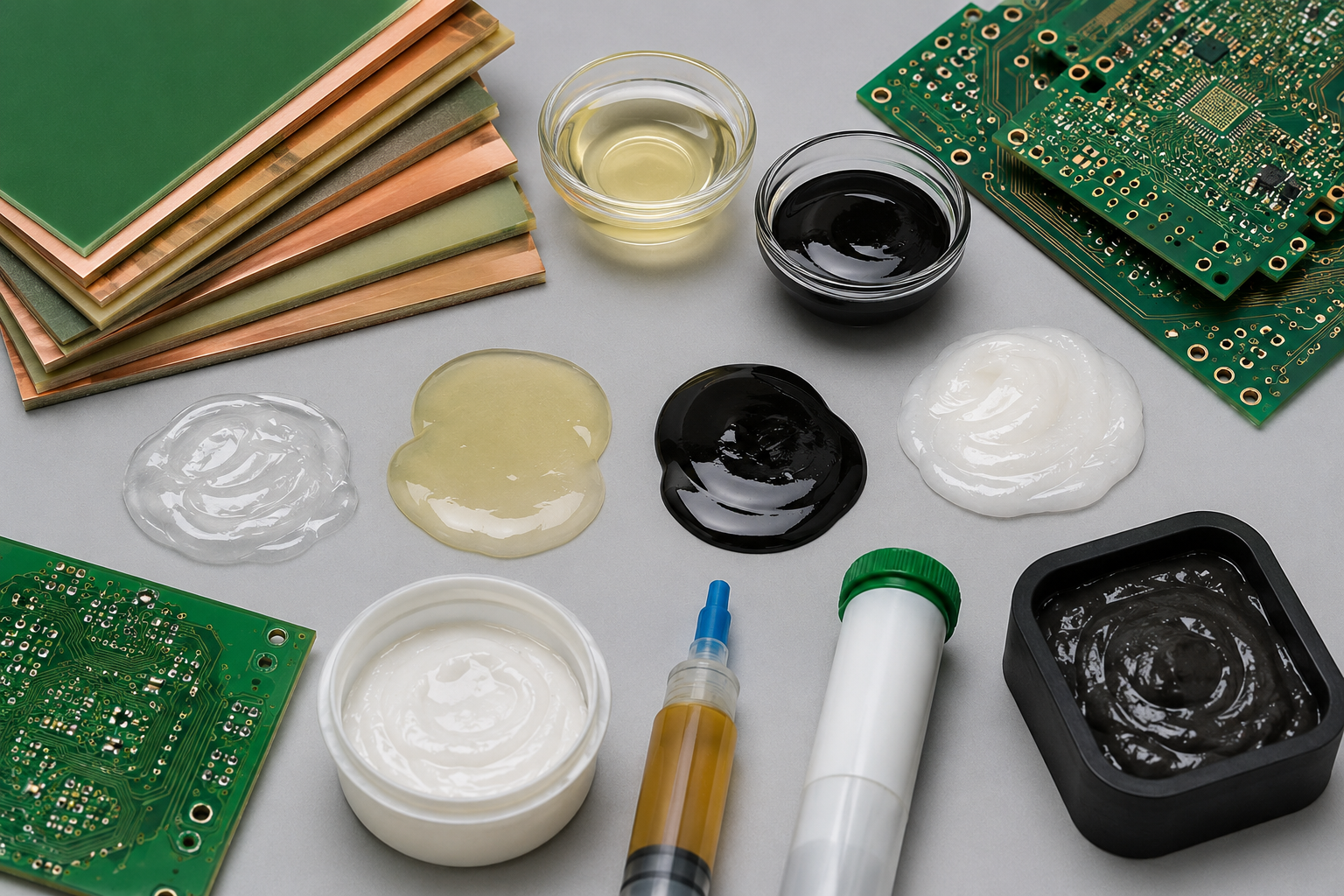
What Materials Are Used in a 104 Capacitor?
A 104 capacitor may use ceramic, plastic film, or other dielectric materials. The dielectric material determines capacitance stability, temperature behavior, voltage response, and long-term reliability.
| Dielectric | Common Characteristics | Typical Use |
|---|---|---|
| X7R | Stable from -55°C to +125°C, general-purpose | Industrial and automotive circuits |
| X5R | Stable from -55°C to +85°C, compact MLCC | Consumer and compact devices |
| Y5V | High capacitance in small size, wider variation | Low-cost non-critical circuits |
| C0G / NP0 | Very stable, low loss | Precision timing and RF circuits |
| Polyester film | Good insulation and stable behavior | General film capacitor use |
| Polypropylene film | Low loss, good AC performance | Power, snubber, and EMI circuits |
For decoupling near ICs, X7R and X5R are common. For precision frequency or timing circuits, C0G/NP0 is better, although 0.1 µF C0G capacitors are usually larger and more expensive.
What Do 104K, 104M, and 104J Mean?
Many capacitors include a letter after the capacitance code. This letter usually indicates capacitance tolerance.
| Marking | Capacitance | Tolerance |
|---|---|---|
| 104J | 0.1 µF | ±5% |
| 104K | 0.1 µF | ±10% |
| 104M | 0.1 µF | ±20% |
| 104Z | 0.1 µF | +80% / -20% |
A 104K capacitor means a 0.1 µF capacitor with ±10% tolerance. A 104M capacitor means the same nominal value with ±20% tolerance.
For decoupling circuits, ±10% or ±20% is often acceptable. For timing, filtering, and frequency-sensitive circuits, tighter tolerance may be required. Buyers should avoid selecting only by “104” because tolerance and dielectric can change the actual circuit performance.
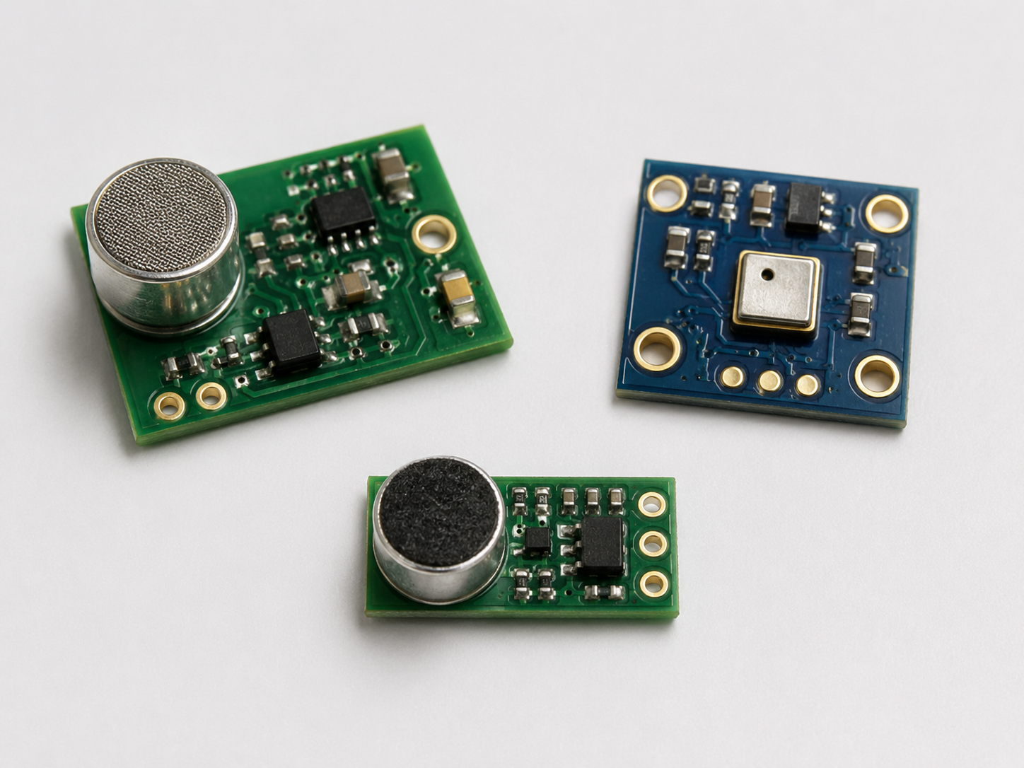
Where Is a 104 Capacitor Used?
The 104 capacitor is used across many electronic products because it fits several basic circuit functions.
| Application | How the 104 Capacitor Helps |
|---|---|
| IC decoupling | Stabilizes voltage near power pins |
| Power rail bypass | Reduces high-frequency noise |
| Signal coupling | Blocks DC while passing AC signal |
| RC timing circuit | Works with a resistor to set delay or timing |
| Sensor module | Reduces noise around signal and supply lines |
| LED driver | Helps improve power stability |
| Motor control board | Suppresses switching noise |
| Communication device | Supports cleaner power for RF and logic circuits |
| Automotive electronics | Helps stabilize control modules |
| Industrial controller | Improves noise immunity in harsh environments |
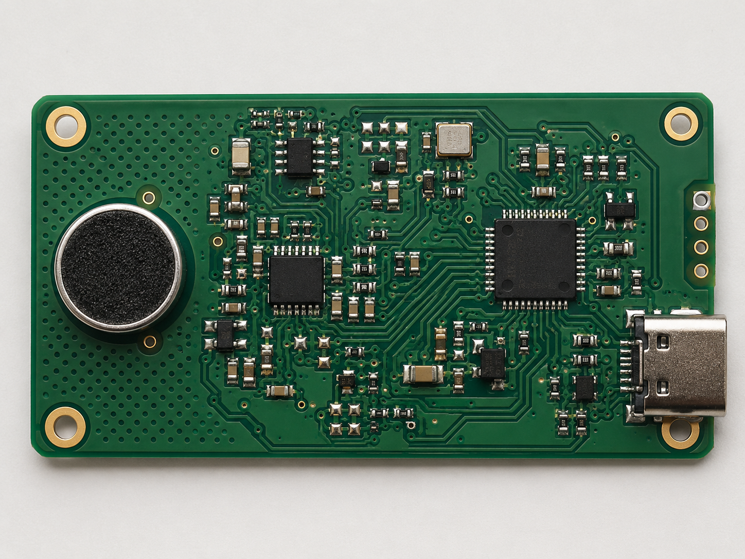
On a PCB, 104 capacitors are often placed near microcontrollers, logic ICs, op-amps, voltage regulators, connectors, and communication chips.
How to Choose the Right 104 Capacitor?
Choosing the right 104 capacitor requires more than confirming the capacitance value. The complete selection should match the electrical, mechanical, thermal, and production requirements of the project.
| Parameter | What to Check |
|---|---|
| Capacitance | 100 nF / 0.1 µF |
| Voltage rating | Higher than actual working voltage with margin |
| Dielectric | X7R, X5R, C0G, film, or safety-rated type |
| Tolerance | ±5%, ±10%, ±20%, or project-specific |
| Package size | 0402, 0603, 0805, 1206, radial, axial, etc. |
| Temperature range | Match operating environment |
| DC bias behavior | Important for MLCC capacitance stability |
| Safety approval | Required for AC mains EMI applications |
| Mounting type | SMT or through-hole |
| Supply status | Check lifecycle, stock, and alternatives |
For a 5V or 12V DC circuit, engineers often select 16V, 25V, or 50V capacitors depending on reliability requirements. For automotive or industrial use, higher voltage margin and better temperature stability are usually preferred.
104 Ceramic Capacitor vs 104 Film Capacitor
A 104 ceramic capacitor and a 104 film capacitor may have the same capacitance value, but they behave differently in real circuits.
| Item | 104 Ceramic Capacitor | 104 Film Capacitor |
|---|---|---|
| Size | Smaller | Larger |
| Cost | Usually lower | Usually higher |
| SMT availability | Very common | Less common than MLCC |
| Stability | Depends on dielectric | Generally good |
| High-frequency response | Good for decoupling | Good for selected AC applications |
| Voltage options | Wide range | Wide range |
| Typical use | PCB decoupling, bypass | Audio, timing, AC, EMI, industrial circuits |
For compact digital boards, ceramic MLCC is usually the first choice. For AC signal circuits, audio paths, timing stability, and some power applications, film capacitors may be preferred.
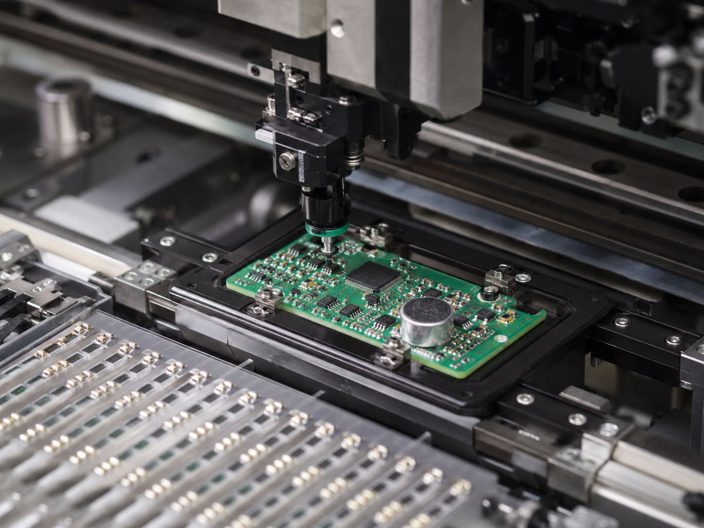
What Should Engineers Notice During PCB Design?
A 104 capacitor works best when the PCB layout supports its function. Poor placement can reduce filtering performance even when the component value is correct.
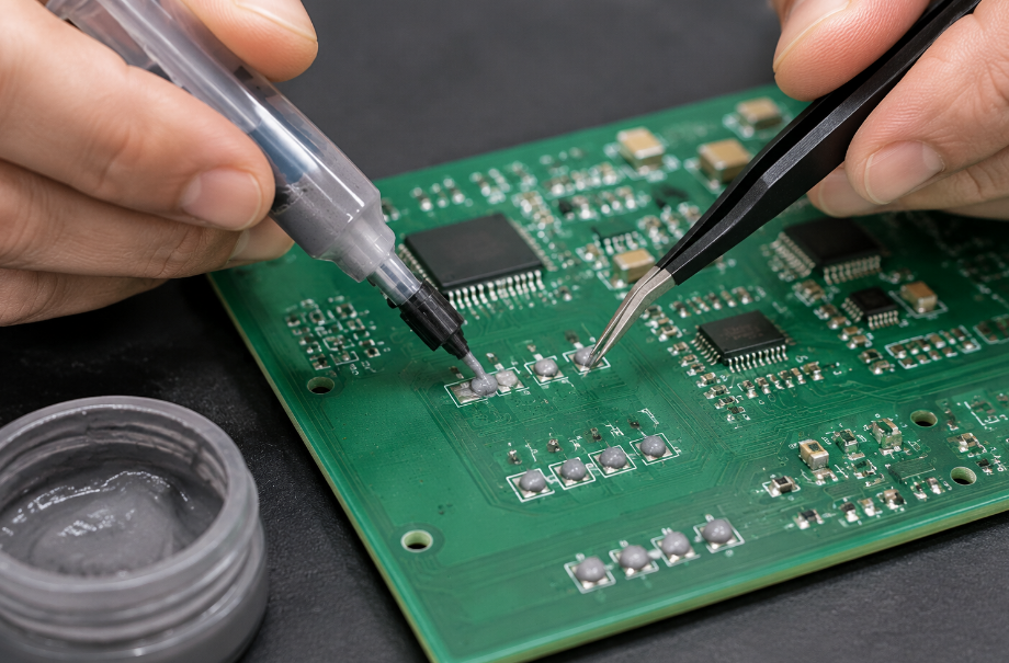
For IC decoupling, place the capacitor as close as possible to the power and ground pins. Keep traces short and wide. Use direct vias to the power and ground planes when possible. Avoid routing the capacitor through long thin traces.
| Design Point | Recommended Practice |
|---|---|
| Placement | Close to IC power pin |
| Ground connection | Short path to ground plane |
| Trace length | As short as practical |
| Via use | Use nearby vias for power and ground |
| Loop area | Keep current loop small |
| Multiple ICs | Use local decoupling for each IC |
| High-speed circuits | Combine 104 with smaller capacitors if needed |
In dense PCB layouts, engineers sometimes place 0402 or 0201 MLCCs directly under or beside IC packages to reduce parasitic inductance.
What Common Problems Can Happen with a 104 Capacitor?
Although the 104 capacitor is simple, several problems can appear during design, sourcing, assembly, or field operation.
| Problem | Possible Cause | Practical Solution |
|---|---|---|
| Poor filtering effect | Capacitor placed too far from IC | Improve layout and reduce loop area |
| Lower actual capacitance | MLCC DC bias effect | Use higher voltage rating or larger package |
| Cracking | Board bending or thermal stress | Improve PCB handling and use soft termination if needed |
| Wrong value assembled | Similar appearance of MLCCs | Use BOM control and incoming inspection |
| Leakage or short | Overvoltage, damage, contamination | Check voltage margin and quality control |
| Noise remains high | Insufficient capacitor network | Add bulk and high-frequency capacitors |
| Failure in AC input | Non-safety capacitor used | Use certified X/Y safety capacitor |
For mass production, capacitor issues are often linked to incorrect substitution, poor storage control, soldering stress, or insufficient verification during BOM replacement.
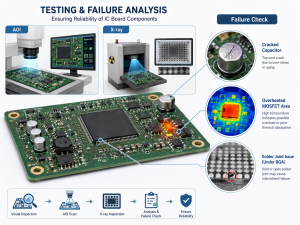
How Is a 104 Capacitor Tested?
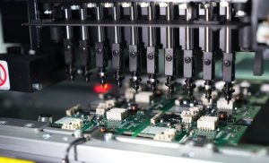
Testing depends on capacitor type and application. For normal PCB assembly, manufacturers may check capacitance, appearance, solderability, polarity if applicable, and placement accuracy. Since most 104 ceramic capacitors are non-polarized and visually similar, BOM control and reel label verification are important.
| Test Method | Purpose |
|---|---|
| Capacitance measurement | Confirms actual capacitance value |
| LCR meter test | Measures capacitance, ESR, and loss factor |
| Visual inspection | Checks cracks, damage, and marking |
| AOI inspection | Confirms placement and solder joint quality |
| X-ray inspection | Checks hidden solder issues if needed |
| ICT test | Verifies assembled circuit connectivity |
| Functional test | Confirms circuit-level performance |
| Reliability test | Checks temperature, humidity, or vibration endurance |
For high-reliability products, capacitor selection should be verified under real operating voltage and temperature, not only at room temperature.
What Affects 104 Capacitor Cost?
The price of a 104 capacitor depends on more than capacitance. Two capacitors with the same “104” marking may have very different costs because of material, voltage rating, size, tolerance, certification, and brand.
| Cost Factor | Impact |
|---|---|
| Dielectric material | C0G and specialty dielectrics cost more |
| Voltage rating | Higher voltage often increases cost |
| Package size | Larger MLCCs may cost more |
| Tolerance | Tight tolerance increases price |
| Safety certification | X/Y capacitors cost more than general types |
| Brand | Authorized brands may have price differences |
| Quantity | Bulk purchasing improves unit cost |
| Supply condition | Shortage or EOL status can raise cost |
| Testing requirement | Extra inspection increases total cost |
For OEM and ODM projects, the best approach is not always choosing the cheapest capacitor. A stable part with reliable supply and suitable electrical margin can reduce rework, field failure, and production delays.
How to Buy 104 Capacitors for Production?
For production purchasing, buyers should confirm the full part specification instead of searching only for “104 capacitor.” The BOM should include capacitance, tolerance, voltage, dielectric, package size, manufacturer part number, and approved alternatives.
| Item | What to Confirm |
|---|---|
| Capacitance | 0.1 µF / 100 nF |
| Tolerance | J, K, M, or specified tolerance |
| Voltage | 16V, 25V, 50V, 100V, or higher |
| Dielectric | X7R, X5R, C0G, film, safety type |
| Package | 0402, 0603, 0805, 1206, radial, etc. |
| Brand | Original manufacturer and traceable source |
| Datasheet | Confirm parameters before approval |
| Certification | RoHS, REACH, AEC-Q200, UL, or safety approval if required |
| Packaging | Tape and reel, bulk, ammo pack, or tray |
| Alternatives | Approved second source for stable supply |
For PCBA factories, component substitution should be reviewed by engineering before production. A replacement with the same capacitance but different dielectric or voltage rating may cause performance changes.
How to Identify a 104 Capacitor Correctly?
Through-hole capacitors may show “104” directly on the body. SMT MLCCs usually have no printed marking because the package is too small. In that case, the value must be identified through reel labels, BOM records, supplier documents, and measurement.
| Method | Suitable For |
|---|---|
| Printed code | Dipped ceramic, film, larger capacitors |
| Reel label | SMT MLCC production parts |
| BOM and MPN | Engineering and procurement control |
| LCR meter | Value confirmation |
| Datasheet check | Full parameter verification |
| Supplier traceability | Quality and authenticity control |
For buyers, visual checking alone is not enough. A 104 capacitor in 0603 X7R 50V may look almost identical to another 0603 capacitor with a different value. Controlled labeling and traceable sourcing are essential.
What Quality Standards Matter for 104 Capacitors?
The required standards depend on the product application. For consumer electronics, RoHS and REACH compliance may be sufficient. For automotive electronics, AEC-Q200-qualified capacitors are commonly preferred. For AC mains EMI suppression, X or Y safety certification is mandatory.
| Requirement | Typical Application |
|---|---|
| RoHS | General electronic products |
| REACH | Export and environmental compliance |
| AEC-Q200 | Automotive electronic components |
| UL / ENEC / VDE | Safety capacitors for AC circuits |
| ISO-controlled sourcing | Production quality management |
| Lot traceability | Industrial, medical, automotive, aerospace projects |
For regulated or high-reliability industries, capacitor traceability should cover supplier source, batch number, incoming inspection, production lot, and shipment record.
FAQs About 104 Capacitor
What is the value of a 104 capacitor?
A 104 capacitor has a value of 100,000 pF, which equals 100 nF or 0.1 µF. The first two digits “10” are the significant numbers, and the third digit “4” means four zeros are added in picofarads.
Is a 104 capacitor the same as 0.1 µF?
Yes. A 104 capacitor is the same as 0.1 µF. It can also be written as 100 nF or 100,000 pF. These are different unit expressions for the same capacitance value.
What is a 104 ceramic capacitor used for?
A 104 ceramic capacitor is commonly used for IC decoupling, power supply bypassing, signal filtering, and noise reduction. It is often placed close to IC power pins to stabilize voltage during fast switching.
What does 104K mean on a capacitor?
104K means the capacitor value is 0.1 µF with a tolerance of ±10%. The “104” indicates capacitance, while the “K” indicates tolerance. Other common tolerance letters include J for ±5% and M for ±20%.
Can I replace a 104 capacitor with another 0.1 µF capacitor?
Usually yes, but the replacement should match voltage rating, dielectric material, tolerance, package size, temperature range, and safety approval if used in AC circuits. Matching capacitance alone is not always enough.
Does a 104 capacitor have polarity?
Most 104 ceramic and film capacitors are non-polarized, so they can be installed in either direction. However, engineers should still check the datasheet because capacitor type and application may vary.
What voltage rating should I choose for a 104 capacitor?
The voltage rating should be higher than the actual working voltage with a suitable margin. For common low-voltage DC circuits, 16V, 25V, or 50V capacitors are often used. Industrial and automotive circuits may require higher ratings.
Is a 104 capacitor good for power supply filtering?
Yes. A 104 capacitor is widely used for high-frequency filtering and decoupling. It often works together with larger capacitors such as 1 µF, 10 µF, or 22 µF to cover a wider noise frequency range.
Why does an MLCC 104 capacitor lose capacitance under DC voltage?
Class II ceramic capacitors such as X5R and X7R can lose effective capacitance under DC bias. The amount depends on voltage rating, package size, dielectric, and applied voltage. Engineers should check datasheet curves for critical designs.
Can a 104 capacitor be used in AC mains circuits?
Only safety-certified capacitors should be used across or from AC mains lines. A general 104 capacitor should not replace an X or Y safety capacitor. For EMI suppression, always choose certified safety-rated components.
What package size is common for SMT 104 capacitors?
Common SMT packages include 0402, 0603, 0805, and 1206. Smaller packages save space, while larger packages may provide better capacitance stability under DC bias and higher voltage ratings.
How can I test a 104 capacitor?
You can test it with an LCR meter or capacitance meter. For production, suppliers and PCBA factories may also use incoming inspection, AOI, ICT, and functional testing to verify assembly quality and circuit performance.
Why are 104 capacitors placed near ICs?
They are placed near ICs to supply short bursts of current and reduce high-frequency voltage noise. Short placement distance lowers parasitic inductance and improves decoupling performance.
What is the difference between 103 and 104 capacitors?
A 103 capacitor is 10,000 pF, or 10 nF. A 104 capacitor is 100,000 pF, or 100 nF. The third digit controls the number of zeros added in picofarads.
How should buyers source 104 capacitors for mass production?
Buyers should source by full manufacturer part number, not only by “104.” The approved specification should include capacitance, voltage, tolerance, dielectric, package, compliance, lifecycle status, and traceable supply source.
Conclusion
A 104 capacitor is a 0.1 µF / 100 nF capacitor used in a wide range of electronic circuits. It is especially valuable for IC decoupling, noise suppression, power rail bypassing, signal filtering, and compact PCB assembly. For engineering teams, the main selection points are voltage rating, dielectric material, tolerance, package size, temperature stability, and real circuit placement. For buyers, the key is to source by full specification and verified part number, not by the “104” marking alone.
For stable production, select approved brands, confirm datasheets, prepare alternative part numbers, and maintain traceable sourcing records. This helps reduce quality risk, avoid production delays, and support long-term product reliability.
If you are looking for reliable OEM manufacturing, ODM production, sample development, mass production, or custom engineering solutions, welcome to contact our engineering team for technical support and quotation service.