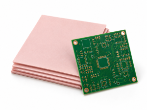
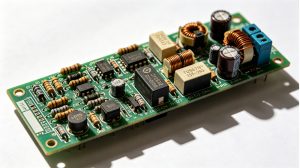
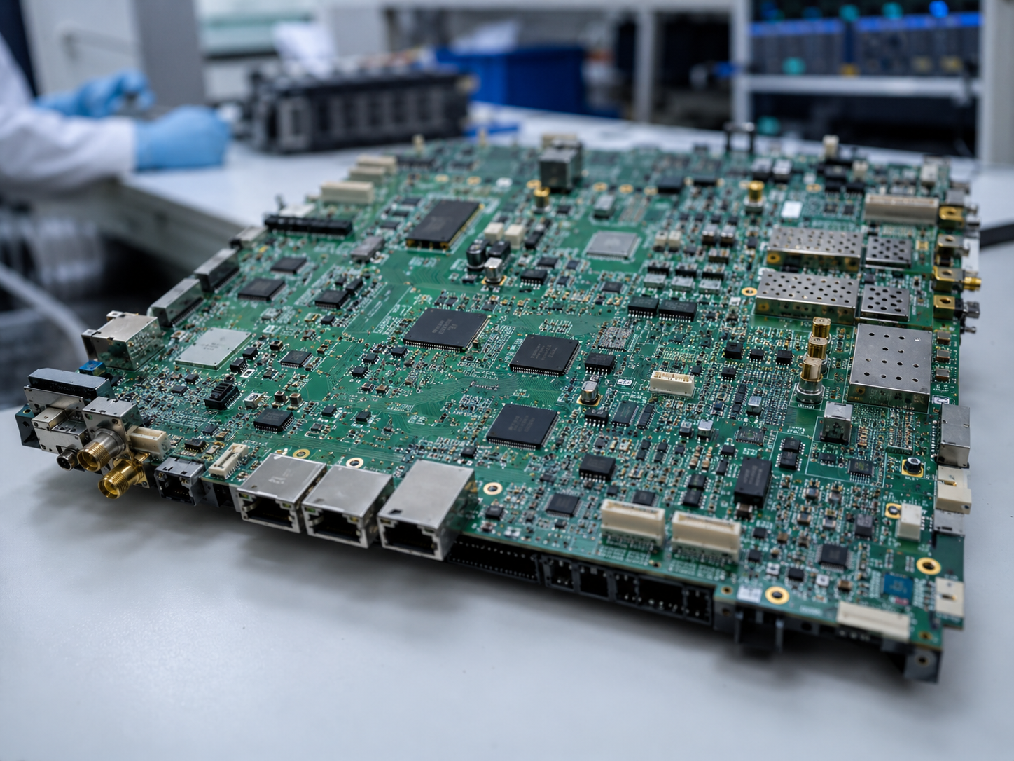
Are you looking for mixed technology PCB assembly that can handle SMT parts and through-hole components on the same board with stable quality and clear delivery control? Many electronic products include compact chips, connectors, relays, terminals, transformers, and other parts that cannot be handled well by SMT alone.
For this reason, mixed technology PCB assembly is widely used in PCBA projects that require both high-density layout and strong mechanical connection. It helps balance board size, solder strength, component flexibility, production cost, and long-term product reliability.
What is Mixed Technology PCB Assembly?
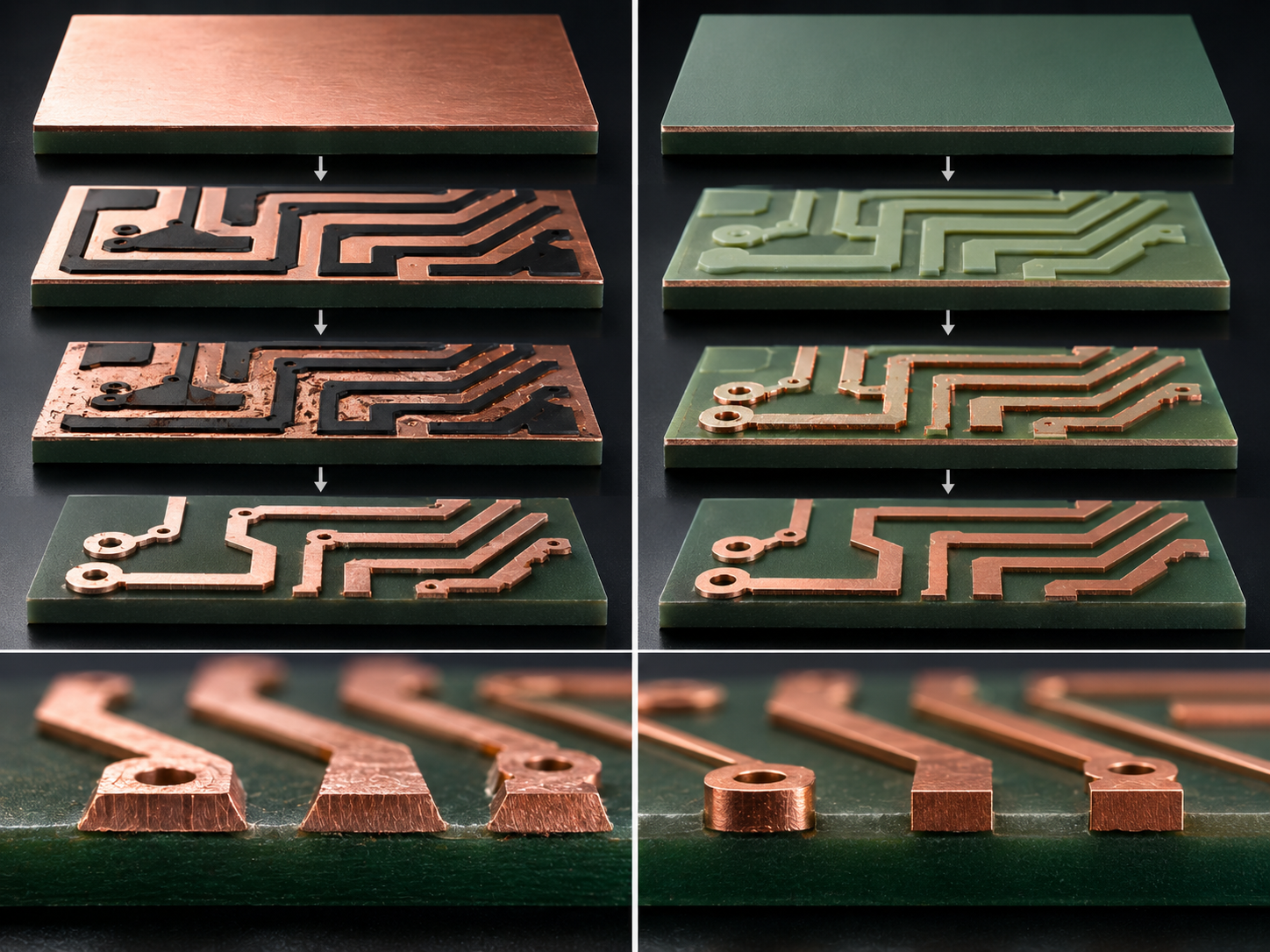
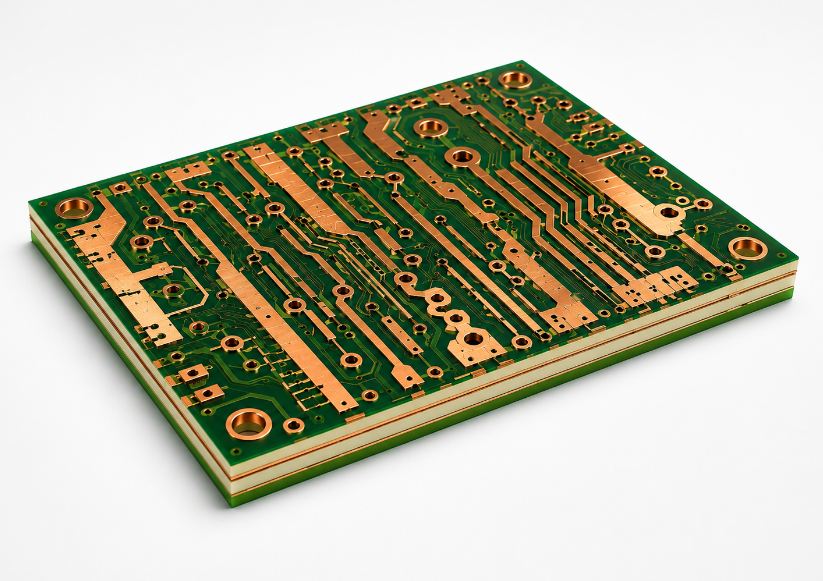
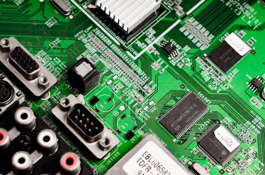
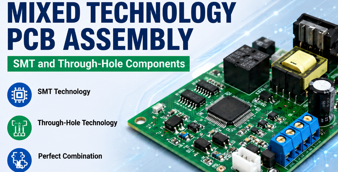
Mixed technology PCB assembly is a PCBA method that combines surface mount technology and through-hole technology on one printed circuit board. SMT parts are mounted directly on PCB surface pads, while through-hole parts are inserted into drilled holes and soldered to the plated hole wall.
This assembly type is used when a board contains both small electronic components and larger mechanical or power-related parts. ICs, resistors, capacitors, LEDs, and sensors often use SMT, while connectors, switches, relays, terminals, transformers, and fuse holders often use through-hole assembly.
Compared with pure SMT assembly, mixed PCB assembly gives more design flexibility. It supports compact circuit layout while keeping stronger solder joints for parts exposed to plugging force, vibration, pulling force, heat, or repeated operation.
Why is Mixed Technology PCB Assembly Used?
Mixed technology pcb assembly is used because some components perform better with through-hole mounting. Large connectors, power terminals, transformers, relays, and switches often require stronger mechanical support than surface pads can provide.
It is also useful when a product combines electronic control, power input, signal transmission, and mechanical interface on the same board. SMT supports compact control circuits, while through-hole assembly supports stronger physical connection points.
Another reason is component availability. Some parts are still easier to source, replace, or qualify in through-hole packages. Mixed SMT THT assembly gives more flexibility when balancing performance, cost, durability, and long-term supply planning.
How is SMT Assembly Different from Through-Hole Assembly?
SMT assembly and through-hole assembly use different mounting methods. SMT parts are placed directly on the PCB surface, while through-hole parts pass through drilled holes and are soldered around the leads.
In mixed technology PCB assembly, these two methods are often combined. SMT helps save space and supports automated placement, while through-hole assembly improves connection strength for larger and stress-bearing components.
| Comparison Item | SMT Assembly | Through-Hole Assembly |
|---|---|---|
| Full Name | Surface Mount Technology Assembly | Through-Hole Technology Assembly |
| Mounting Method | Components are mounted directly on PCB surface pads | Component leads are inserted through plated holes |
| PCB Design Requirement | Requires accurate solder paste pads and placement coordinates | Requires drilled holes, annular rings, and proper hole-to-lead ratio |
| Component Size | Usually smaller and lighter | Usually larger and heavier |
| Board Space Usage | Saves more PCB space and supports compact design | Takes more space because holes and leads occupy board area |
| Component Density | Suitable for high-density circuit layouts | Lower component density due to hole spacing limits |
| Assembly Speed | Fast and highly automated with pick-and-place machines | Slower because insertion and soldering require more handling |
| Soldering Process | Mainly uses reflow soldering | Uses wave soldering, selective soldering, or manual soldering |
| Mechanical Strength | Suitable for small and low-stress components | Stronger for parts exposed to vibration, pulling, or plugging force |
| Electrical Performance | Suitable for high-speed and compact signal circuits | Suitable for higher current, power, and stronger connection points |
| Typical Components | ICs, resistors, capacitors, LEDs, diodes, sensors, small packages | Connectors, relays, terminal blocks, transformers, switches, fuse holders |
| Automation Level | High automation, suitable for mass production | Lower automation, depending on component type and process |
| Production Cost | Usually lower for high-volume compact boards | May be higher due to insertion, soldering, and inspection time |
| Inspection Method | AOI, SPI, X-ray for hidden joints such as BGA | Visual inspection, solder joint inspection, ICT, functional testing |
| Repair and Rework | Small parts may require special tools and skilled operation | Larger parts are usually easier to replace or repair |
| Reliability Advantage | Good for compact, lightweight, and high-speed electronics | Good for durable connections and high-stress operating conditions |
| Common Limitation | Not ideal for large or mechanically stressed parts | Not ideal for ultra-compact or high-density layouts |
| Best Application | Consumer electronics, communication boards, control modules, compact PCBA | Power boards, industrial control, interface boards, heavy-duty electronic products |
| Role in Mixed Assembly | Handles most small electronic components efficiently | Supports large, durable, or mechanically stressed components |
For many modern boards, the best approach is not choosing only SMT or only through-hole assembly. A mixed SMT THT assembly approach keeps the PCB compact while strengthening important connection points.
When Should You Choose Mixed Technology Instead of SMT Assembly?
Mixed technology PCB assembly is a better choice when the board includes parts that are not suitable for SMT mounting. These may include power connectors, mechanical switches, transformers, terminal blocks, fuse holders, relays, and heavy capacitors.
It is also suitable for products exposed to vibration, frequent plugging, high current, external force, or long operating cycles. Industrial control boards, power boards, communication modules, automotive electronics, medical electronics, and equipment controllers often use mixed assembly.
Mixed assembly is also useful when a design contains specific through-hole packages. Instead of changing the whole design, PCBA mixed assembly allows SMT and THT components to work together in one controlled production flow.
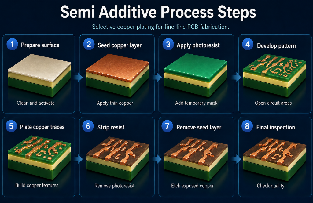
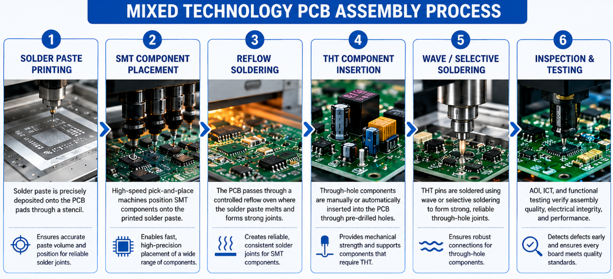
What Is the Mixed Technology PCB Assembly Process?
The mixed technology PCB assembly process must follow a clear production sequence because SMT parts and through-hole parts use different mounting and soldering methods. In most projects, SMT assembly is completed first, then through-hole components are inserted and soldered.
Step 1: Review Production Files
The factory checks Gerber files, BOM, pick-and-place files, assembly drawings, polarity marks, and testing requirements. This step confirms PCB structure, component package, part quantity, mounting position, and soldering method.
For mixed PCB assembly, the review should also check hole size, pad design, component spacing, connector direction, and whether nearby SMT parts may affect through-hole soldering.
Step 2: Confirm DFM and Assembly Sequence
DFM review confirms whether the PCB layout is suitable for SMT and THT assembly. Key points include SMT pad size, through-hole diameter, annular ring, solder mask opening, component clearance, and soldering access.
The assembly sequence is then confirmed. Usually, SMT is assembled first, followed by through-hole insertion and soldering. This prevents large THT parts from blocking SMT placement or inspection.
Step 3: Prepare PCBs and Components
Bare PCBs are checked for surface finish, warpage, cleanliness, solder mask quality, drilled holes, and panel design. Components are checked by part number, quantity, package, polarity, and storage condition.
SMT parts should be prepared in reels, trays, tubes, or cut tape for machine placement. Through-hole parts should be checked for lead length, lead shape, body size, and insertion direction.
Step 4: Print Solder Paste
Solder paste is printed onto SMT pads through a stencil. Paste volume must match pad size and component type to avoid solder bridging, insufficient solder, or poor wetting.
Stencil thickness, aperture design, paste release, and printing pressure should be controlled, especially for fine-pitch ICs, QFN, BGA, and small passive components.
Step 5: Place SMT Components
Pick-and-place machines mount SMT components according to the coordinate file. The placement program controls part position, rotation, package type, and feeder location.
Accurate placement is important for small components and fine-pitch parts. Misalignment may cause open joints, bridging, or component shifting during reflow.
Step 6: Reflow Soldering
The PCB passes through a reflow oven, where solder paste melts and forms solder joints between SMT terminals and PCB pads. The temperature profile must match PCB thickness, copper weight, solder paste type, and component heat tolerance.
Poor reflow control may cause tombstoning, solder balls, cold joints, voids, or damaged components.
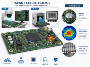
Step 7: SMT Inspection
After reflow, AOI checks missing parts, wrong polarity, skewed components, solder bridging, insufficient solder, and open joints. X-ray inspection may be used for BGA, QFN, or hidden solder joints.
SMT inspection should be completed before through-hole insertion because large THT parts may block inspection or make repair harder.
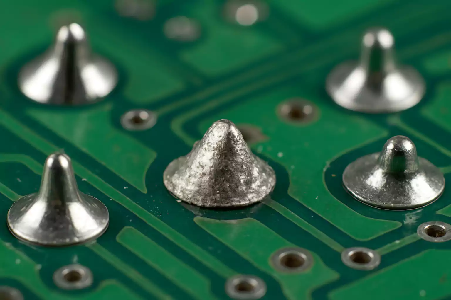
Step 8: Insert Through-Hole Components
Through-hole components are inserted after SMT inspection. Common parts include connectors, terminal blocks, relays, transformers, switches, fuse holders, and electrolytic capacitors.
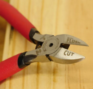
Insertion may be manual or automated. Component direction, seating height, lead fit, and mechanical clearance should be checked before soldering.
Step 9: Solder Through-Hole Components
Through-hole soldering can use wave soldering, selective soldering, or manual soldering. The choice depends on component quantity, PCB layout, nearby SMT parts, soldering area, and production volume.
Wave soldering suits boards with many THT parts and enough clearance. Selective soldering suits local soldering areas near SMT components. Manual soldering suits special parts, low-volume runs, repairs, or components unsuitable for automated soldering.
Step 10: Clean and Inspect the Board
After THT soldering, the board is checked for solder joint shape, barrel fill, lead trimming, component height, polarity, flux residue, and tilted parts.
Cleaning depends on flux type and product requirement. For no-clean flux, cleaning may not be required unless appearance, coating, or reliability standards require it.
Step 11: Electrical and Functional Testing
Testing may include continuity test, ICT, functional test, power-on test, programming, communication test, or custom fixture test. The exact test depends on circuit function and product application.
For PCBA mixed assembly, testing is important because the board may include power input, signal connectors, control circuits, and mechanical interface components.
Step 12: Final Inspection and Packing
Final inspection checks board appearance, quantity, labels, connector direction, component condition, and packing requirements. Boards are packed with ESD protection, foam, trays, or moisture-proof bags when required.
This process helps control soldering quality, reduce rework, and support stable delivery for mixed technology PCB assembly projects.
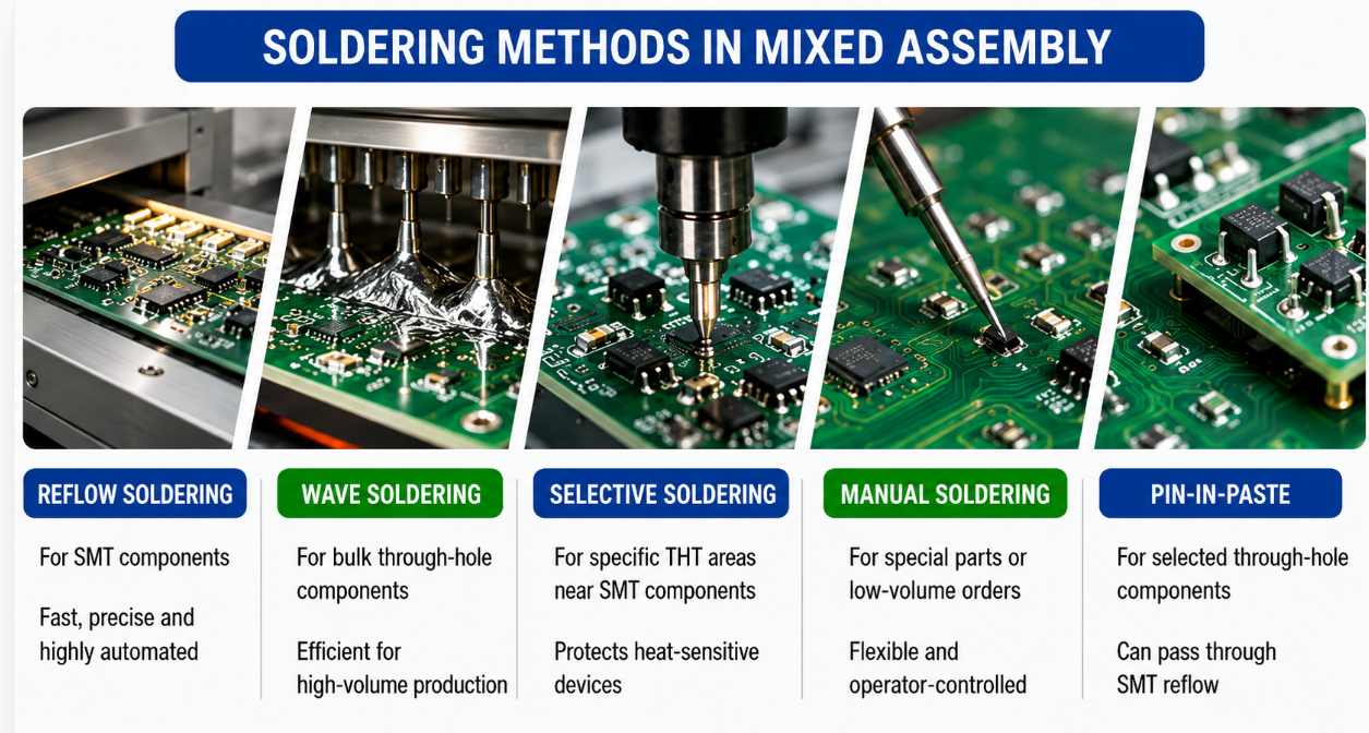
What Soldering Methods Are Used in Mixed Technology PCB Assembly?
Mixed technology PCB assembly may use several soldering methods because SMT and through-hole components do not always share the same soldering process. The suitable method depends on component type, layout density, heat sensitivity, production volume, and solder joint requirements.
| Soldering Method | Suitable For | Main Advantage | Common Limitation |
|---|---|---|---|
| Reflow Soldering | SMT components | Fast and accurate for surface mount parts | Not suitable for most through-hole parts |
| Wave Soldering | Many through-hole parts | Efficient for batch THT soldering | Requires enough spacing and fixture control |
| Selective Soldering | Local through-hole areas | Protects nearby SMT parts | Requires accurate process programming |
| Manual Soldering | Special parts or low-volume orders | Flexible for complex areas | Slower and operator-dependent |
| Pin-in-Paste | Selected through-hole parts | Can pass through SMT reflow | Requires correct hole and paste volume design |
In most mixed SMT THT assembly projects, SMT reflow is finished first. Through-hole soldering is then completed by wave, selective, or manual soldering based on layout and component structure.
DFM Guidelines for Mixed Technology PCB Assembly
DFM review for mixed technology PCB assembly should focus on layout clearance, soldering access, hole design, pad design, test access, and assembly sequence. These items directly affect solder joint quality, production speed, repair difficulty, and final PCBA reliability.
1. Keep Enough Space Between SMT and THT Parts
Small SMT parts should not be placed too close to connectors, relays, transformers, terminal blocks, or electrolytic capacitors. Large THT parts may block pick-and-place nozzles, AOI cameras, soldering tools, and rework access.
For dense layouts, keep clear space around fine-pitch ICs, BGA, QFN, and 0201/0402 components. If a large THT component must be placed nearby, confirm that inspection and repair tools can still reach the SMT solder joints.
2. Match Through-Hole Diameter with Lead Size
Through-hole diameter should match the actual lead diameter after considering tolerance and plating thickness. A hole that is too tight may cause difficult insertion, bent leads, PCB damage, or cracked plated holes.
A hole that is too large may reduce solder filling and weaken the joint. For connectors, switches, terminals, and relays, the hole design must support both solder flow and mechanical holding strength.
3. Design Enough Annular Ring for THT Pads
THT pads should have enough annular ring around the drilled hole. If the annular ring is too narrow, the pad may lift during soldering or repair, especially on connectors and parts that receive external force.
For high-stress components, larger pads can improve solder fillet strength. Connector pins, terminal blocks, fuse holders, and heavy components should not use minimum pad sizes unless space is extremely limited.
4. Optimize SMT Pad Size and Paste Opening
SMT pads should match the component package and solder paste volume. For fine-pitch ICs, QFN, BGA, and small passive parts, stencil apertures may require reduction to prevent solder bridging.
For 0201, 0402, and small chip components, pad balance is important. Unequal pad size or uneven copper connection may cause tombstoning, part shifting, or insufficient solder after reflow.
5. Reserve Soldering Clearance Around THT Areas
If wave soldering is used, there should be enough clearance around THT solder joints to avoid solder bridging and shadowing. Small SMT parts should not sit directly behind large THT leads in the solder flow direction.
If selective soldering is used, the nozzle must have enough working space around each solder point. Connectors, tall parts, and nearby components should not block the nozzle path.
6. Confirm Component Height and Mechanical Interference
Tall components such as transformers, electrolytic capacitors, relays, connectors, switches, and heat sinks should be checked against enclosure height, cable space, screw holes, and final product structure.
Mechanical keep-out areas should be marked clearly. Parts near board edges, mounting holes, clips, shells, or cables must leave enough space for assembly and final installation.
7. Place Heat-Sensitive Components Away from Soldering Heat
Plastic connectors, switches, sensors, LEDs, batteries, and heat-sensitive ICs should not be placed too close to wave soldering, selective soldering, or manual soldering points.
If heat-sensitive parts must be near THT solder joints, the soldering process should be reviewed before production. Selective soldering or manual soldering may be safer than full wave soldering in tight areas.
8. Arrange Components According to Assembly Sequence
The layout should support the real production order. In most mixed PCB assembly projects, SMT is assembled first, then THT parts are inserted and soldered.
Large THT parts should not be mounted before SMT inspection. Otherwise, they may block AOI cameras, X-ray access, rework tools, and test probes.
9. Keep Test Points Accessible After Assembly
Test points should not be hidden under connectors, transformers, relays, heat sinks, or tall capacitors. ICT probes, programming pins, and functional test fixtures must touch the required pads after all components are installed.
Test points should have enough spacing and stable surface finish. If the board requires programming, power-on testing, or communication testing, test pads should be placed where fixtures can reach them easily.
10. Mark Polarity and Connector Direction Clearly
Polarity marks should be clear for LEDs, diodes, ICs, electrolytic capacitors, connectors, batteries, and polarized THT parts. Pin 1 marks should be visible on both the silkscreen and assembly drawing.
Connector direction should be marked clearly when similar connectors are used on the same board. This helps prevent reverse insertion, wrong cable direction, and incorrect final assembly.
11. Avoid Weak Board Edge and Mounting Hole Layouts
Heavy connectors, switches, or terminals should not be placed too close to unsupported board edges unless mechanical support is added. Repeated plugging or pulling may stress the solder joints and PCB laminate.
Mounting holes should keep enough clearance from copper, pads, traces, and tall components. Screws, washers, and fixtures should not touch exposed conductors or damage nearby parts.
12. Provide Complete Assembly Notes Before Quotation
Mixed technology PCB assembly should include Gerber files, BOM, pick-and-place file, assembly drawing, polarity notes, soldering requirements, test requirements, and special handling instructions.
If any component requires manual soldering, special height control, lead forming, glue fixing, conformal coating, or separate packing, it should be stated before quotation. This helps avoid price changes and production delays after order confirmation.
What Common Defects Should Be Avoided in Mixed Technology PCB Assembly?
Mixed technology PCB assembly involves SMT placement, reflow soldering, through-hole insertion, and THT soldering. Defects may come from pad design, hole size, soldering sequence, component handling, or poor inspection control.
1. Solder Bridging
Solder bridging often appears between fine-pitch SMT pins, connector pins, or dense through-hole leads. Common causes include excessive solder paste, narrow pad spacing, poor stencil opening, or unsuitable wave soldering direction.
To reduce this risk, stencil aperture design, pad spacing, solder mask clearance, and soldering profile should be checked before production. Dense THT pins should also be reviewed when wave soldering is planned.
2. Insufficient Solder
Insufficient solder may occur on SMT pads, through-hole barrels, connector pins, and terminal blocks. It can cause weak electrical contact, unstable signal transmission, or poor mechanical strength.
For SMT parts, the solder paste volume should match pad size and component package. For through-hole parts, hole size, lead diameter, soldering temperature, and contact time should be controlled.
3. Poor Barrel Fill
Poor barrel fill is a common through-hole soldering defect. It means solder does not properly fill the plated hole, which can reduce both electrical connection and mechanical strength.
This issue is often related to wrong hole-to-lead ratio, poor preheating, low solder temperature, short soldering time, or poor PCB plating quality. It is especially important for connectors, relays, terminals, and high-current parts.
4. Tombstoning
Tombstoning usually happens to small chip components such as 0201, 0402, and 0603 packages. One side of the component lifts during reflow, creating an open circuit.
Common causes include unbalanced pad size, uneven copper connection, uneven heating, or different solder wetting speeds on both ends. Pad symmetry and thermal balance should be checked during DFM review.
5. Component Misalignment
Misalignment may happen during SMT placement or through-hole insertion. SMT parts may shift during reflow, while THT parts may lean, float, or fail to sit flat on the board.
This defect can affect soldering quality, appearance, enclosure fit, and connector alignment. Placement coordinates, component footprint, fixture design, and insertion height should be checked before assembly.
6. Cold Solder Joints
Cold solder joints usually look dull, rough, or incomplete. They may appear when soldering temperature is too low, contact time is too short, or the solder surface is contaminated.
Cold joints can create intermittent electrical failure. Reflow profile, wave soldering temperature, selective soldering parameters, and manual soldering control should be verified.
7. Lifted Pads or Damaged Plated Holes
Lifted pads and damaged holes may appear during rework, manual soldering, or forced component insertion. This is more likely when THT holes are too tight or pads are too small.
Connectors, switches, and terminals should have proper pad size and annular ring. Components that receive external force should not rely on weak minimum-size pads.
8. Wrong Polarity or Wrong Orientation
Polarity errors often happen on diodes, LEDs, ICs, electrolytic capacitors, connectors, and polarized through-hole components. Similar connectors on the same board may also be inserted in the wrong direction.
Clear silkscreen marks, Pin 1 marks, assembly drawings, and first article inspection help prevent this issue. Directional parts should always be checked before batch assembly.
9. Flux Residue and Contamination
Flux residue may remain around THT pins, connectors, dense SMT areas, or manual soldering points. If the board requires conformal coating or high-reliability operation, residue may affect appearance, insulation, or long-term stability.
Cleaning should be selected according to flux type and product requirement. No-clean flux may still require cleaning when coating, testing, or appearance standards require a cleaner surface.
10. Blocked Test Points
Test points may become blocked by tall capacitors, relays, connectors, heat sinks, cables, or transformers. Once blocked, ICT, programming, or functional testing may become difficult.
Test points should be checked after all SMT and through-hole components are installed. Fixture access should be confirmed before production, not after assembly is complete.
What Quality Control Is Needed for Mixed-Technology PCB Assembly?
Quality control for mixed technology pcb assembly should cover file review, material inspection, SMT process control, through-hole soldering inspection, electrical testing, and final shipment checks. Each stage should be controlled separately because SMT and THT defects are different.
1. Production File Review
Gerber files, BOM, pick-and-place files, assembly drawings, polarity notes, and test requirements should be checked before production. This step helps confirm footprint, component package, quantity, orientation, soldering method, and special process requirements.
For mixed PCB assembly, file review should also check through-hole size, pad spacing, connector direction, soldering clearance, and whether tall components may block inspection or test access.
2. Incoming PCB Inspection
Bare PCBs should be checked for board size, surface finish, solder mask quality, drilled holes, plating quality, warpage, cleanliness, and panel structure. Hole quality is especially important for through-hole soldering.
If the board has tight spacing, high copper weight, BGA, or dense mixed assembly areas, extra attention should be given to solder mask opening, pad accuracy, and surface flatness.
3. Component Verification
Components should be checked by part number, package, quantity, polarity, moisture sensitivity, and storage condition. SMT parts should match machine feeding formats such as reel, tray, tube, or cut tape.
Through-hole parts should be checked for lead diameter, lead length, lead shape, body size, and insertion direction. Odd-form parts should be confirmed before production to avoid insertion or fixture problems.
4. First Article Inspection
First article inspection confirms whether the first assembled board matches the BOM, placement file, polarity requirements, and assembly drawing. It is useful before batch production starts.
This step should cover SMT parts, THT parts, connectors, directional components, component height, and soldering appearance. Errors found at this stage are easier to correct than after full production.
5. SMT Process Inspection
SMT quality control includes solder paste printing, component placement, reflow profile, and AOI inspection. SPI may be used when solder paste volume control is critical.
AOI should check missing components, wrong orientation, skewed parts, bridging, insufficient solder, and wrong values when visible. X-ray may be used for BGA, QFN, or hidden solder joints.
6. Through-Hole Soldering Inspection
After THT soldering, solder joints should be checked for barrel fill, wetting, solder bridge, lead trimming, component seating, polarity, and connector direction.
For wave soldering and selective soldering, process parameters should be controlled carefully. For manual soldering, operator consistency and soldering appearance should be checked more strictly.
7. Electrical and Functional Testing
Testing may include continuity testing, ICT, programming, power-on testing, communication testing, and functional testing. The test method should match the board function and product application.
Mixed SMT THT assembly often includes connectors, power input, signal interfaces, switches, and control circuits. Functional testing helps confirm that all assembly areas work together correctly.
8. Final Inspection and Packing Check
Final inspection should confirm board appearance, solder joint condition, component height, connector alignment, label content, quantity, and packing method.
Packing should use ESD-safe bags, trays, foam, moisture-proof bags, or custom protection when required. This helps reduce damage during storage and transport.
What Factors Affect the Cost of Mixed-Technology PCB Assembly Services?
The cost of mixed technology PCB assembly services depends on board complexity, component quantity, SMT/THT ratio, soldering method, inspection level, testing scope, order quantity, and delivery schedule.
Boards with many fine-pitch SMT parts and many through-hole components usually take more process time. Loose parts, odd-form parts, large connectors, transformers, and relays may also increase handling and fixture cost.
Testing also affects price. AOI, X-ray, ICT, functional testing, conformal coating, programming, and box assembly add value, but they also increase total project cost. Complete files help create a more accurate quotation.
| Cost Factor | Impact on Price |
|---|---|
| PCB Size and Panel Design | Affects handling, fixture, and production efficiency |
| Component Count | More parts increase placement and inspection time |
| SMT/THT Ratio | More through-hole parts often raise labor and soldering cost |
| Soldering Method | Selective soldering and manual soldering may cost more |
| Component Package | Loose or odd-form parts require extra handling |
| Testing Level | ICT, FCT, and X-ray increase inspection cost |
| Lead Time | Faster delivery may require priority scheduling |
| Quantity | Higher volume can reduce unit cost |
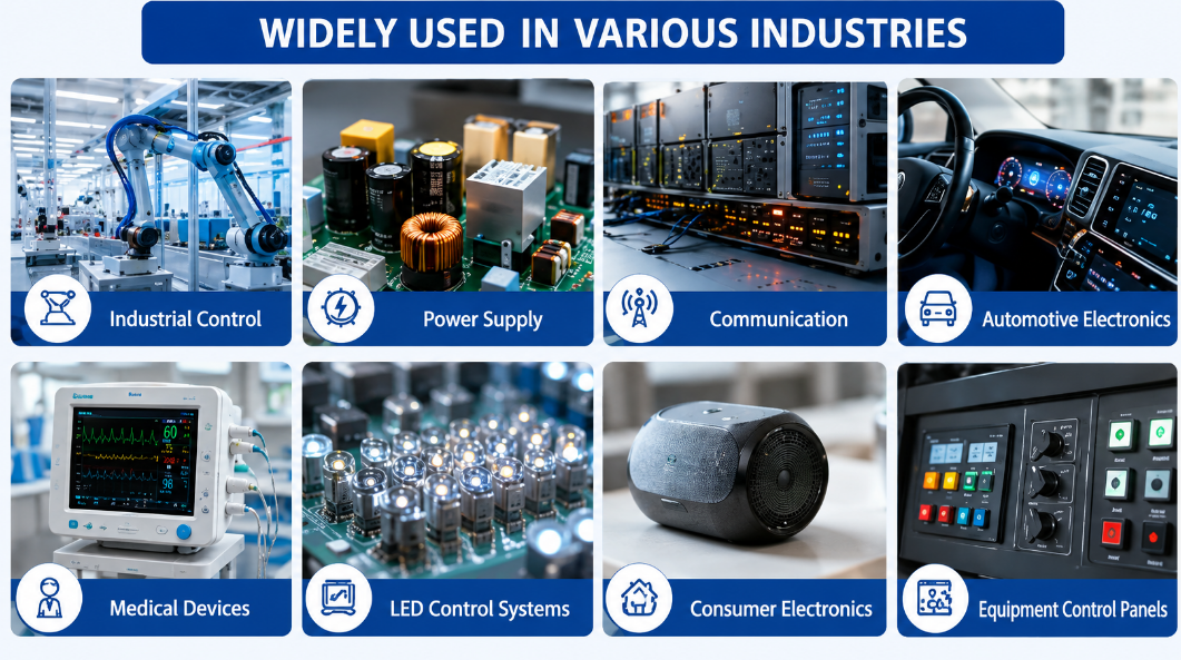
Where Is Mixed Technology PCB Assembly Commonly Used?
Mixed technology PCB assembly is used when one PCB must combine compact SMT circuits with strong through-hole connection points. It is common in products that require stable signal control, power connection, mechanical strength, and long service life.
1. Industrial Control Boards
Industrial control boards often include ICs, resistors, sensors, terminal blocks, relays, and power connectors. SMT supports compact control circuits, while through-hole parts provide stronger connection for wiring and field installation.
2. Power Supply and Power Control Boards
Power boards often use transformers, inductors, fuse holders, electrolytic capacitors, terminals, and high-current connectors. These parts usually require through-hole mounting for better mechanical support and current handling.
3. Communication Equipment
Communication boards may combine SMT chips, RF modules, signal circuits, connectors, and interface ports. Mixed assembly helps support compact layout while keeping stable external connection points.
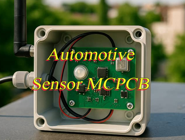
4. Automotive Electronics
Automotive electronic modules may face vibration, temperature change, and repeated operation. Mixed PCB assembly is often used for control modules, sensor boards, lighting controllers, power interfaces, and connector-heavy boards.
5. Medical Electronic Devices
Medical electronics may require compact circuits, stable connectors, reliable power input, and consistent testing. Mixed SMT THT assembly can support both small signal components and durable interface parts.
6. Consumer Electronics and Smart Devices
Some consumer products use SMT for compact circuit areas and through-hole parts for charging ports, switches, connectors, speakers, or high-stress interface components.
7. LED Control Systems
LED control boards may include SMT control ICs, resistors, capacitors, terminal blocks, connectors, and power input parts. Mixed assembly supports both control function and practical field wiring.
8. Equipment Control Panels
Control panels may include switches, connectors, displays, indicators, buzzers, and control ICs. Through-hole parts help strengthen user-facing components, while SMT parts keep the circuit compact.
What Files Are Required for Mixed Technology PCB Assembly Quotation?
A clear quotation requires complete production files. Missing or unclear files may cause price changes, production delay, wrong components, or assembly risk.
Gerber files define PCB layers, copper, solder mask, silkscreen, drill data, and board outline. The BOM lists component part number, quantity, package, value, manufacturer, and approved substitute parts.
Pick-and-place files help confirm SMT coordinates and rotation. Assembly drawings are also important because they show polarity, connector direction, through-hole insertion, height limits, and testing points.
Quotation file checklist:
- Gerber files
- BOM with full part numbers
- Pick-and-place file
- Assembly drawing
- PCB specification
- Testing requirements
- Firmware or programming instructions
- Special packing requirements
- Approved substitute component list
How to Choose Reliable Mixed Technology PCB Assembly Services?
Choosing reliable mixed technology PCB assembly services should focus on process capability, quality control, sourcing support, testing ability, and delivery stability. Since mixed assembly includes both SMT and through-hole processes, the supplier must control more than simple component placement.
Check SMT and THT Assembly Capability
The supplier should support SMT placement, reflow soldering, through-hole insertion, wave soldering, selective soldering, and manual soldering. This ensures the board can be assembled according to component type, layout density, and soldering requirement.
Confirm DFM Review Before Production
A reliable supplier should review pad size, hole diameter, annular ring, soldering clearance, component height, polarity marks, and test point access before production. This helps reduce solder defects, rework, and quotation changes.
Review Component Sourcing Support
Mixed PCB assembly may include SMD parts, connectors, relays, terminals, BGA, QFN, QFP, and odd-form components. Strong sourcing support helps control cost, lead time, and substitute part risks.
Check Inspection and Testing Options
The supplier should provide AOI, visual inspection, X-ray when needed, ICT, functional testing, or custom fixture testing. Testing requirements should be confirmed before quotation to avoid later cost or schedule changes.
Confirm Prototype and Batch Production Support
Prototype production verifies component fit, soldering method, test access, and functional performance. Batch production requires stable process control, repeatable inspection standards, and clear delivery planning.
Evaluate Communication and Delivery Control
A good supplier should provide clear file review feedback, quotation details, lead time, production updates, and delivery plan. This is important for mixed SMT THT assembly because PCB fabrication, component sourcing, assembly, testing, and packing must be coordinated together.
Why Choose EBest for Mixed Technology PCB Assembly Services?
EBest is suitable for mixed technology PCB assembly services because it supports PCB fabrication, component sourcing, SMT assembly, through-hole assembly, mixed assembly, testing support, and box assembly in one service system.
One-Stop PCB and PCBA Service
EBest supports PCB fabrication, component supply, SMT assembly, through-hole assembly, full turnkey PCB assembly, prototype PCB assembly, quick turn PCB assembly, BGA assembly, flex PCB assembly, ceramic PCB assembly, and box assembly.
SMT, THT, and Mixed Assembly Capability
EBest supports SMT, THT, and mixed assembly. It can handle SMD parts, through-hole components, BGA packages, QFN/QFP packages, connectors, relays, terminals, and components supplied in reels, cut tape, tubes, trays, or loose parts.
Strong Production Capability
EBest lists a placement capacity of 13,200,000 chips per day, minimum SMD component size of 01005, minimum BGA pitch of 0.25mm, maximum component size of 50 × 150mm, and bare board size support from 0.2 × 0.2 inches to 20 × 20 inches / 22 × 47.5 inches.
Fast Assembly Lead Time
EBest lists PCBA assembly lead time of 1–5 days and also supports expedite service for urgent PCB projects. Final lead time depends on file readiness, component availability, board complexity, and testing requirements.
Certified Quality Support
EBest is supported by ISO 9001:2015, ISO 13485:2016, IATF 16949, AS9100D, REACH, RoHS, and UL certifications. These certifications support quality control for industrial, medical, automotive, aerospace, and commercial electronics.
Component Sourcing and Value-Added Support
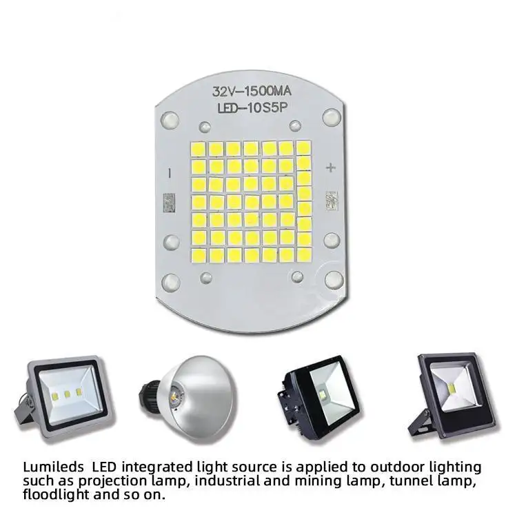
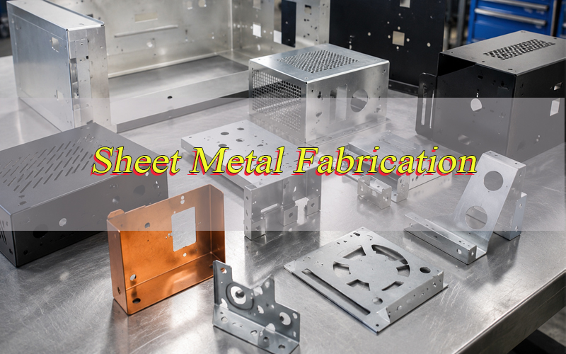
EBest provides component sourcing for SMD, BGA, QFN, QFP, and other electronic components. It can also support box assembly, injection molding, CNC machining, sheet metal, and final assembly for projects that require more than PCBA production.
FAQs About Mixed Technology PCB Assembly
Q1: Can a PCB have SMT parts on both sides and through-hole parts on one side?
A1: Yes. Many mixed assembly boards use double-sided SMT and one-sided through-hole insertion. The process sequence must be reviewed carefully so heavy parts, soldering heat, and inspection access do not create assembly problems.
Q2: Is selective soldering better than wave soldering for mixed assembly?
A2: Selective soldering is often better for dense boards because it solders local THT points without exposing the whole board to a solder wave. Wave soldering is more efficient when many THT parts are grouped with enough clearance.
Q3: What causes through-hole solder joints to be weak?
A3: Weak THT solder joints may come from oversized holes, poor barrel fill, low solder temperature, short soldering time, contaminated surfaces, or insufficient pad size. Connector and terminal areas should be checked carefully during DFM review.
Q4: Can mixed assembly support BGA components?
A4: Yes. BGA components can be assembled with SMT before THT insertion. X-ray inspection is usually recommended because BGA solder joints are hidden under the package.
Q5: Should through-hole parts be inserted before or after SMT assembly?
A5: In most cases, through-hole parts are inserted after SMT reflow and SMT inspection. This prevents large THT parts from blocking pick-and-place machines, AOI cameras, X-ray access, and rework tools.
Q6: What information helps get a more accurate mixed assembly quote?
A6: A complete quotation package should include Gerber files, BOM, pick-and-place file, assembly drawing, testing requirements, special soldering notes, component sourcing requirements, and packing instructions.
Q7: Can mixed technology PCB assembly be used for small batches?
A7: Yes. It is suitable for prototypes, small batches, and volume production. Small-batch production is useful for checking component fit, soldering quality, test method, and product function before larger orders.
Q8: What should be checked before approving mass production?
A8: First article inspection, soldering appearance, polarity, connector direction, component height, test results, packing method, and any approved process changes should be confirmed before moving to batch production.
Get a Reliable Mixed Technology PCB Assembly Quote
If your board combines SMT parts, through-hole components, connectors, BGA packages, or functional testing, EBest can support custom mixed technology pcb assembly services. From PCB fabrication and component sourcing to assembly, inspection, testing, and final delivery, EBest helps simplify the full PCBA process.
Send your Gerber files, BOM, pick-and-place file, assembly drawing, and testing requirements to sales@bestpcbs.com. EBest can review your project, confirm the suitable assembly process, and provide a clear quotation for high-quality, reliable, and on-time PCBA delivery.