In electronics, the distinctions between PMOS and NMOS transistors, and how these differences impact circuit performance, PCB design, and manufacturing costs, are important to understand. This article covers their definitions, core differences, working principles, threshold voltage, switching speed, power consumption, identification methods, and more for full clarity.
What are PMOS and NMOS Transistors?
PMOS and NMOS transistors are two fundamental types of MOSFETs (Metal-Oxide-Semiconductor Field-Effect Transistors), the building blocks of modern integrated circuits and PCB designs. Both rely on an electric field to control the flow of current, but they differ in their conductive carriers, substrate doping, and operational requirements. Understanding their basic definitions is critical for avoiding design errors and ensuring circuit reliability.
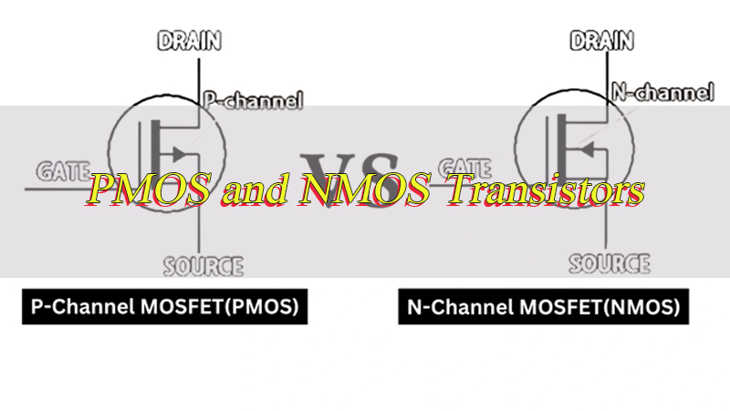
PMOS, short for P-Channel MOSFET, uses holes as its primary conductive carriers. It is constructed on an N-type silicon substrate, with P-type doped source and drain regions. For a PMOS transistor to conduct, the gate voltage must be lower than the source voltage typically a negative voltage relative to the source for enhancement-mode devices, which are the most commonly used in modern circuits. When the gate voltage meets this requirement, a P-type channel forms between the source and drain, allowing current to flow through the device.
NMOS, or N-Channel MOSFET, uses electrons as its primary conductive carriers. It is built on a P-type silicon substrate, with N-type doped source and drain regions. Unlike PMOS, an NMOS transistor conducts when the gate voltage is higher than the source voltage usually a positive voltage relative to the source for enhancement-mode devices. This positive gate voltage creates an N-type channel between the source and drain, enabling electron flow and turning the device on. NMOS transistors are widely used in high-speed and low-resistance applications due to the higher mobility of electrons compared to holes.
What is the Difference between PMOS and NMOS Transistors?
PMOS and NMOS are two core types of MOSFETs, differing primarily in their conductive carriers, substrate doping, and operational requirements. PMOS uses holes as carriers, operates on an N-type substrate, and requires a negative gate voltage to turn on, while NMOS uses electrons, is built on a P-type substrate, and needs a positive gate voltage. These differences lead to variations in switching speed, power consumption, and cost, making each suitable for distinct circuit roles. Below is a comparsion chart between PMOS and NMOS transistors:
| Characteristic | PMOS Transistors | NMOS Transistors |
| Conductive Carrier | Holes (positive charge carriers) | Electrons (negative charge carriers) |
| Substrate Doping Type | N-type silicon substrate | P-type silicon substrate |
| Source/Drain Doping Type | P-type doped regions | N-type doped regions |
| Turn-On Gate Voltage | Gate voltage (VGS) lower than source voltage (typically negative for enhancement-mode) | Gate voltage (VGS) higher than source voltage (typically positive for enhancement-mode) |
| Switching Speed | Slower, due to lower hole mobility (≈480 cm²/V·s) | Faster, due to higher electron mobility (≈1350 cm²/V·s) |
| On-Resistance (RDS(on)) | Higher, even for the same size and voltage rating | Lower, making it ideal for high-current applications |
| Threshold Voltage (Vth) | Negative value (typically -1V to -4V for enhancement-mode) | Positive value (typically 1V to 4V for enhancement-mode) |
| Power Consumption | Higher static power consumption in standalone circuits | Lower static power consumption in standalone circuits |
| Manufacturing Cost | Slightly higher, due to more complex doping processes | Lower, simpler doping process and higher production volume |
| Circuit Role | Ideal for high-side switching, simpler drive without bootstrap circuits | Ideal for low-side switching, high-speed logic, and high-current paths |
How Do PMOS and NMOS Transistors Work in Circuits?
Both PMOS and NMOS transistors operate by controlling the formation of a conductive channel between the source and drain using a gate voltage. The key difference lies in the type of channel formed and the voltage required to activate it. Below is a step-by-step breakdown of how each works in typical circuit configurations.
NMOS Transistor Operation
NMOS is built on a P-type substrate. When no voltage is applied to the gate (VGS = 0), there is no conductive channel between the source and drain, so the device is off. When a positive gate voltage (higher than the positive threshold voltage Vth) is applied relative to the source, an electric field forms, creating an N-type conductive channel. Electrons flow through this channel from source to drain, turning the transistor on. A higher positive gate voltage (above Vth) increases current flow.
PMOS Transistor Operation
PMOS uses an N-type substrate. When VGS = 0, it is off with no conductive channel. To turn it on, a negative gate voltage (lower than the negative threshold voltage Vth) is needed relative to the source. This voltage attracts positive holes, forming a P-type conductive channel. Holes flow from source to drain through the channel, and a more negative gate voltage (below Vth) increases current flow.
Cut-Off State for Both Devices
NMOS is off when the gate voltage is lower than its positive Vth (no channel forms). PMOS is off when the gate voltage is higher than its negative Vth (insufficient to form a channel). In both cases, only minimal leakage current flows, which helps reduce standby power consumption.
What Are the Threshold Voltage Differences Between PMOS and NMOS Transistors?
Threshold voltage (Vth) is the minimum gate-source voltage required to turn a MOSFET on and form a conductive channel. It is a critical parameter that directly impacts circuit design, as it determines the drive voltage needed for the transistor. The threshold voltage differs significantly between PMOS and NMOS transistors, both in polarity and typical values.
| Parameter | PMOS Transistors | NMOS Transistors |
| Polarity of Vth | Negative (Vth < 0) | Positive (Vth > 0) |
| Typical Vth Range (Enhancement-Mode) | -1V to -4V (absolute value 1V to 4V) | 1V to 4V |
| Key Factors Affecting Vth | 1. N-type substrate doping concentration (higher doping increases Vth absolute value) 2. Gate oxide thickness (thicker oxide increases Vth absolute value) 3. Gate material work function (polysilicon doping adjusts Vth) 4. Oxide-charge density (excess charges alter Vth) | 1. P-type substrate doping concentration (higher doping increases Vth) 2. Gate oxide thickness (thicker oxide increases Vth) 3. Gate material work function (polysilicon doping adjusts Vth) 4. Oxide-charge density (excess charges alter Vth) |
| Impact of Vth on Circuit Design | Requires negative gate drive relative to source; lower absolute Vth allows operation with lower drive voltages but increases leakage current | Requires positive gate drive relative to source; lower Vth enables low-voltage operation but increases leakage current |
| Threshold Voltage Variation | Higher variation in manufacturing, especially for large-area devices | Lower variation, more consistent performance across production batches |
Why Is PMOS Slower Than NMOS Transistors in Switching Speed?
A common question is why PMOS transistors are slower than NMOS transistors in switching speed. The answer lies in the fundamental properties of their conductive carriers and device structure. Below are the key reasons, explained in practical terms in electronics.
- Carrier Mobility Difference: The primary reason for the speed gap is the difference in carrier mobility. Electrons, the carriers in NMOS, have a mobility of approximately 1350 cm²/V·s in silicon. Holes, the carriers in PMOS, have a mobility of only about 480 cm²/V·s less than half that of electrons. This means electrons move much faster through the conductive channel than holes, allowing NMOS transistors to switch on and off more quickly. The mobility difference directly translates to faster current switching, which is critical for high-frequency circuits.
- On-Resistance (RDS(on)) Impact: PMOS transistors have higher on-resistance than NMOS transistors of the same size and voltage rating. Higher on-resistance means more voltage drop across the device when conducting, which slows down the charging and discharging of parasitic capacitances in the circuit. These capacitances (such as gate-source and drain-source capacitance) must be charged and discharged during switching, and higher resistance extends the time required for this process, increasing switching delay.
- Threshold Voltage Effects: PMOS transistors have negative threshold voltages, which requires more precise gate drive control. The negative gate voltage needed to turn on PMOS can introduce delays in the drive circuit, especially in mixed-signal designs. NMOS, with its positive threshold voltage, is easier to drive with standard logic levels, reducing drive circuit delays and improving overall switching speed.
- Device Sizing Constraints: To compensate for lower mobility, PMOS transistors often need to be larger than NMOS transistors to achieve similar current-carrying capacity. Larger devices have higher parasitic capacitances, which further slow down switching. Even with larger size, PMOS can rarely match the switching speed of NMOS, making NMOS the preferred choice for high-speed applications like CPU logic gates and signal switching.
Which Has Lower Power Consumption: PMOS vs NMOS Transistors?
Power consumption is a critical consideration in all PCB designs, especially portable and battery-powered devices. The power consumption of PMOS and NMOS transistors differs based on their operating mode, device characteristics, and circuit configuration. Below is a detailed breakdown of which device has lower power consumption and why.
- Static Power Consumption: Static power is the power consumed when the transistor is in a steady state (either fully on or fully off). NMOS transistors have lower static power consumption than PMOS in standalone configurations. When off, both devices have minimal leakage current, but PMOS leakage current is slightly higher due to the lower mobility of holes and higher on-resistance. When on, PMOS requires more power to maintain current flow because of its higher on-resistance more power is dissipated as heat, increasing static power draw.
- Dynamic Power Consumption: Dynamic power is the power consumed during switching (when the transistor transitions from on to off or vice versa). Dynamic power depends on switching speed, parasitic capacitance, and supply voltage. Since NMOS switches faster than PMOS, it has lower dynamic power consumption in most cases. Faster switching reduces the time the transistor spends in the transition state, where power dissipation is highest. Additionally, NMOS has lower parasitic capacitance for the same size, further reducing dynamic power.
- Circuit Configuration Impact: In standalone circuits (using only PMOS or only NMOS), NMOS consistently has lower power consumption. However, when used together in complementary configurations (like CMOS), power consumption is minimized. In CMOS circuits, one transistor (PMOS or NMOS) is always off in steady state, resulting in near-zero static power. This is why CMOS is the preferred logic family for low-power designs, but individually, NMOS still outperforms PMOS in power efficiency.
- Leakage Power Considerations: Leakage power is a subset of static power and becomes critical in low-voltage, high-density designs. PMOS transistors have higher leakage current than NMOS, especially at lower threshold voltages. This leakage current increases static power consumption, making NMOS a better choice for designs where standby power is a priority, such as battery-powered sensors and portable electronics.
How to Tell if a Transistor is NMOS or PMOS Easily?
Being able to quickly identify whether a transistor is NMOS or PMOS is essential for troubleshooting, prototyping, and component replacement. Below are methods to distinguish between them, no complex equipment required in most cases.
- Check the Transistor Part Number: Most manufacturers mark NMOS and PMOS clearly in the part number. NMOS parts usually have an “N” (e.g., IRFZ44N, AO3400A), while PMOS parts have a “P” (e.g., IRF9540, BSS84P). Some series follow fixed rules—IRF9xxx is PMOS, IRLZ series is NMOS, and AO34xx has N channel (00-04) and P channel (07-09) variants. If unsure, cross-check with the datasheet.
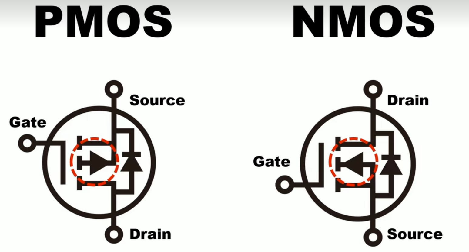
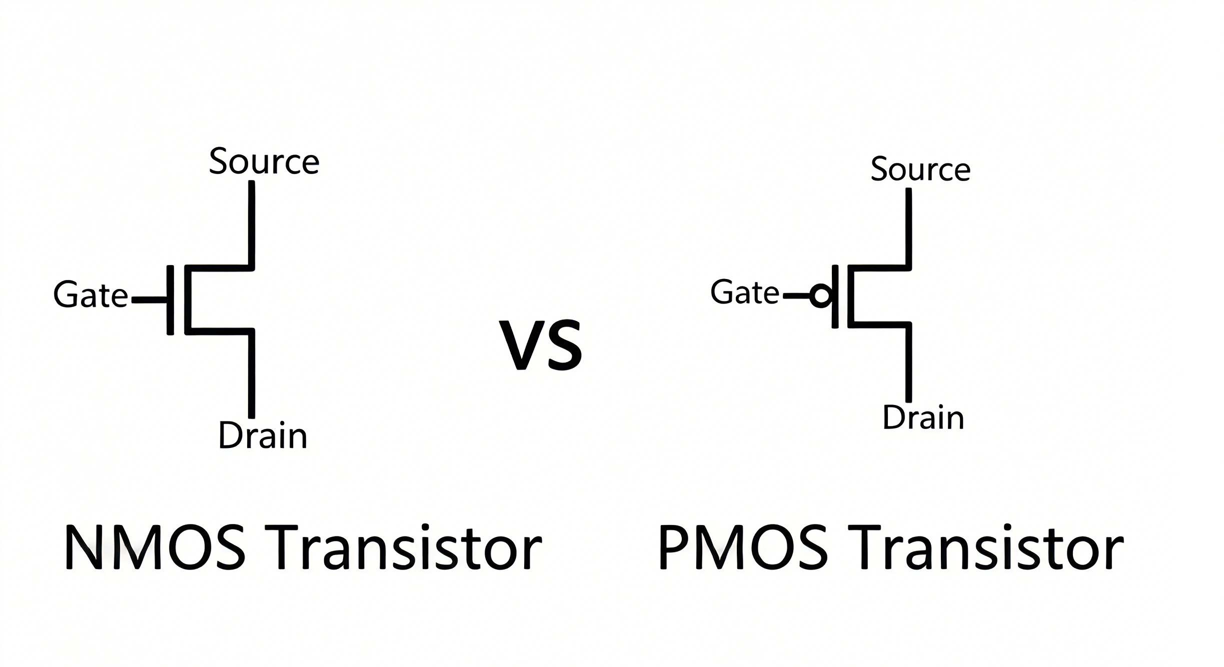
- Examine the Circuit Symbol: When using schematics, the symbol is a quick visual guide. NMOS symbols have an arrow pointing toward the channel, while PMOS symbols have an arrow pointing away. For simple three-pin symbols, the arrow is on the source: arrow toward the gate = NMOS, arrow away = PMOS (memory trick: “arrow in = N, arrow out = P”).
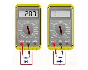
- Test with a Multimeter (Diode Mode): For physical transistors, use a multimeter in diode mode. Test voltage drops between pins, when a 0.4-0.9V drop appears, the red probe is on the source and black on the drain. NMOS shows 0.4-0.6V (silicon) or 0.15-0.3V (Schottky); PMOS shows >1.2V or open circuit with red on source (swap probes to see 0.4-0.9V).
- Check Threshold Voltage (Vth) in the Datasheet: The datasheet’s electrical characteristics list Vth. NMOS has a positive Vth (1V to 4V for enhancement-mode), while PMOS has a negative Vth (-1V to -4V). The datasheet may also label “Carrier” type: electrons for NMOS, holes for PMOS.
- Compare On-Resistance: For transistors of the same size and voltage rating, PMOS has higher on-resistance than NMOS. If you can measure resistance between source and drain when the transistor is on, lower resistance means NMOS, and higher resistance means PMOS.
- Check Pin Configuration Habits: Many manufacturers follow consistent pin layouts. For TO-220 packaged transistors, NMOS often has a source-drain-gate (SDG) order, while PMOS may have source-gate-drain (SGD). This is a preliminary check—always confirm with the datasheet.
- Observe Circuit Application: NMOS is often used for low-side switching (connected to ground) and high-speed circuits, while PMOS is preferred for high-side switching (connected to positive supply) without extra bootstrap circuits. The transistor’s position in the circuit can hint at its type.

Can PMOS and NMOS Transistors Be Used Together in the Same Circuit?
Yes, PMOS and NMOS transistors can be used together in the same circuit, and this combination is the foundation of modern digital and analog design. Theircomplementary strengths make up for each other’s limitations, and they are widely applied in various circuit designs.
The key to their combined use lies in their complementary operating characteristics: NMOS excels in low-side switching, high speed, and low on-resistance, while PMOS is more suitable for high-side switching with simpler drive circuits (no bootstrap circuit needed). For example, in load switch applications, NMOS can be used as a low-side switch connected to the ground for fast switching, and PMOS as a high-side switch connected to the power supply for easy drive control, achieving efficient current control with minimal power loss.
Which Logic Family Uses Both PMOS and NMOS Transistors?
The logic family that uses both PMOS and NMOS transistors is CMOS (Complementary Metal-Oxide-Semiconductor). CMOS is widely used in modern electronics, with its advantages of low power consumption, high noise immunity, and wide operating voltage range derived from the complementary pairing of PMOS and NMOS.
A CMOS logic gate consists of one PMOS and one NMOS transistor connected in series between the positive supply voltage (VDD) and ground (VSS), with their gates connected as the input. When input is high, NMOS turns on and PMOS turns off (output low); when input is low, PMOS turns on and NMOS turns off (output high).This complementary operation ensures no direct current path between VDD and VSS in steady state, resulting in minimal static power consumption.
Common CMOS variants include 4000 series, 74HC series, 74AC series, and CMOS-SOI for high-frequency use. All rely on the complementary PMOS-NMOS structure, outperforming NMOS-only or PMOS-only logic families in power consumption and noise immunity.
When designing with CMOS, PMOS and NMOS transistors must be properly matched to avoid shoot-through current and propagation delay. CMOS devices are ESD-sensitive, so ESD protection should be added to PCB designs.
Are PMOS and NMOS Transistors Different in Manufacturing Cost?
NMOS transistors are slightly cheaper to manufacture than PMOS. The cost difference mainly comes from doping process complexity, production volume, and yield rates.
NMOS is cheaper because its doping process is simpler: it is built on a standard P-type silicon substrate, with N-type source/drain regions formed by implanting phosphorus or arsenic ions, this process is straightforward and has high yield rates. Additionally, NMOS has higher production volume due to its widespread use in high-speed and high-current applications, further reducing per-unit costs.
PMOS is more expensive due to more complex manufacturing: it requires an N-type substrate (less common, needing an extra step to convert standard P-type substrate), and its P-type source/drain regions use boron ion implantation, more sensitive to process variations than NMOS’s phosphorus/arsenic implantation. These factors increase complexity, reduce yield rates, and raise costs.
The cost difference is typically 5-15%, which adds up in high-volume designs. However, PMOS’s unique advantages (e.g., simple high-side switching) often justify the extra cost; engineers usually prioritize performance over cost, but understanding the difference is key for budget-conscious designs.
How to Choose Between PMOS and NMOS Transistors for PCB Design?
Choosing between PMOS and NMOS transistors for PCB design depends on several key factors, including switching speed, power consumption, circuit topology, drive requirements, and cost. A structured approach to selecting the right transistor type for each application ensures optimal performance and reliability.
- Prioritize Switching Speed: If a design requires high switching speeds (e.g., logic gates, high-frequency signal switching, or PWM circuits), choose NMOS. NMOS’s higher electron mobility and lower on-resistance make it significantly faster than PMOS. For applications where switching speed is critical (like CPU cores or high-speed data interfaces), NMOS is the only practical choice.
- Consider Power Consumption: For low-power designs (e.g., battery-powered devices, sensors, or standby circuits), NMOS is preferred due to its lower static and dynamic power consumption. If the design uses a complementary configuration (like CMOS), the combination of PMOS and NMOS will deliver the lowest possible power consumption, but individual low-power switching should still use NMOS.
- Evaluate Circuit Topology: High-side switching (switch connected to the positive supply voltage) is easier with PMOS, as it does not require a bootstrap circuit. NMOS can be used for high-side switching but requires a gate drive voltage higher than the supply voltage, adding complexity. Low-side switching (switch connected to ground) is best with NMOS, as it has lower on-resistance and simpler drive requirements.
- Assess Drive Requirements: NMOS requires a positive gate voltage relative to the source, which is compatible with standard logic levels (e.g., 3.3V or 5V), making drive circuits simple. PMOS requires a negative gate voltage relative to the source, which may require additional components (like level shifters) to generate the necessary drive voltage, increasing circuit complexity.
- Factor in Current-Carrying Capacity: For high-current applications (e.g., power supplies, motor drives, or load switches), NMOS is better due to its lower on-resistance. PMOS can carry current but requires a larger device size to match NMOS’s current capacity, increasing PCB space and cost.
- Consider Cost and Availability: NMOS transistors are cheaper and more widely available than PMOS, making them the default choice for most designs where performance requirements allow. PMOS should only be used when its unique advantages (like simple high-side switching) are necessary, as it will add slightly to the component cost.
- Check Voltage Ratings: Ensure the transistor’s drain-source voltage (VDS) and gate-source voltage (VGS) ratings match the circuit’s operating voltage. NMOS and PMOS have similar voltage ratings, but some high-voltage applications may have more NMOS options available, making it easier to find a suitable component.
FAQ About PMOS vs NMOS Transistors
Q1: Can I replace a PMOS transistor with an NMOS transistor in my circuit?
A1: No, you cannot directly replace a PMOS transistor with an NMOS transistor.PMOS and NMOS have opposite polarities for threshold voltage and drive requirements: PMOS requires a negative gate voltage relative to the source, while NMOS requires a positive gate voltage. Direct replacement will cause circuit failure, as the transistor will not turn on or off correctly. To substitute, choose a PMOS with matching voltage, current, and on-resistance ratings, or redesign the drive circuit to accommodate an NMOS (e.g., adding a bootstrap circuit for high-side switching).
Q2: Do PMOS and NMOS transistors have different ESD sensitivity?
A2: Both PMOS and NMOS are ESD-sensitive, but PMOS is slightly more sensitive. The thin gate oxide layer in both is vulnerable to ESD, but PMOS’s N-type substrate and P-type source/drain regions have a lower ESD breakdown voltage. To protect both, add ESD protection diodes or TVS in PCB design and follow ESD safety protocols during assembly and handling.
Q3: Why do PMOS transistors have higher on-resistance than NMOS?
A3: PMOS has higher on-resistance due to lower hole mobility compared to electron mobility in NMOS. Holes move at ~480 cm²/V·s, while electrons move at ~1350 cm²/V·s. Lower mobility leads to higher resistance in the PMOS conductive channel, even for the same device size and voltage rating. To reduce on-resistance, PMOS must be made larger than NMOS, increasing PCB space and cost.
Q4: Can PMOS and NMOS transistors be used in high-voltage applications?
A4: Yes, both have high-voltage variants (up to several hundred volts), but NMOS is more commonly used.NMOS has lower on-resistance and faster switching speed, making it more suitable for high-voltage scenarios. High-voltage PMOS is available but more expensive with higher on-resistance. For high-voltage designs, choose transistors with VDS ratings exceeding the maximum circuit voltage and use proper heat sinking.
Q5: How does temperature affect PMOS and NMOS transistor performance?
A5: Temperature impacts both, but in similar ways for key parameters. For NMOS: threshold voltage decreases, increasing leakage current and reducing switching speed. For PMOS: absolute threshold voltage decreases, also increasing leakage current. On-resistance increases with temperature for both, as carrier mobility decreases. In high-temperature environments, use transistors with matching temperature ratings and derate current/voltage for reliability.
Q6: What is the role of the substrate in PMOS and NMOS transistors?
A6: The substrate is the base silicon layer forming the transistor’s foundation. For NMOS: substrate is P-type, typically connected to source or ground to prevent parasitic conduction. For PMOS: substrate is N-type, typically connected to source or positive supply voltage. The substrate’s doping type determines the conductive channel type (N-type for NMOS, P-type for PMOS) and affects threshold voltage and leakage current.
Q7: Are there any applications where PMOS is better than NMOS?
A7: Yes, PMOS is better for high-side switching applications.PMOS does not require a bootstrap circuit for gate driving, making the drive circuit simpler and more reliable. For example, in load switches connected to the positive supply, PMOS can be turned on by pulling the gate to ground (a simple logic signal). PMOS is also useful in low-noise analog circuits, as its lower switching noise improves signal integrity.