5G network deployment in 2026 is no longer just about adding more base stations or showing a larger coverage map. The industry has moved into a more selective and technical phase, where operators, enterprises, and equipment manufacturers care about network capability, service quality, energy efficiency, monetization, and hardware reliability.
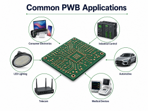
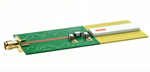
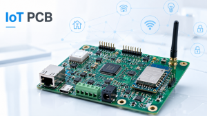
The first wave of 5G focused on consumer mobile broadband. It includes 5G Standalone cores, private industrial networks, fixed wireless access, Open RAN, network slicing, AI-assisted operations, non-terrestrial networks, and 5G-Advanced features. These changes also create new requirements for telecom hardware, including RF modules, antenna systems, high-speed PCB, high-frequency PCB, HDI PCB, ceramic PCB, thermal substrates, and reliable PCBA assembly.

What Does 5G Network Deployment Mean in 2026?
5G network deployment in 2026 means building a complete connectivity system, not only installing radio equipment.
A modern 5G rollout includes the radio access network, antennas, baseband units, transport network, edge computing nodes, core network, cloud platforms, cybersecurity layers, service orchestration, and user devices. In early deployments, many operators used 5G Non-Standalone architecture, where the 5G radio network still depended on the existing 4G core. That helped operators launch faster, but it limited some of the deeper capabilities of 5G.
By 2026, the meaning has expanded. A serious 5G project may include:
- 5G Standalone core migration
- Mid-band and mmWave densification
- Private 5G for industrial sites
- Fixed wireless access for home and business broadband
- Network slicing for differentiated service packages
- AI-based planning and network optimization
- Edge computing for low-latency applications
- Open RAN or Cloud RAN architecture
- Satellite-assisted coverage for remote regions
- More reliable RF and high-speed electronic hardware
This is why 5G deployment is now closer to a full infrastructure transformation than a simple radio upgrade.
Why Is 5G Network Deployment Entering a New Phase?
5G deployment is entering a new phase because operators are moving from coverage expansion to value creation.
In the early stage, the main target was simple: launch 5G service, promote faster mobile speed, and compete in consumer markets. That was important, but it did not fully use the technical potential of 5G. Many operators now need a clearer business return from their network investment. They want services that can support enterprise automation, premium connectivity, industrial IoT, fixed broadband, cloud gaming, smart transportation, and mission-critical applications.
This change brings a different deployment logic. Instead of only asking “Where can we expand coverage?”, operators now ask:
- Which cities or industries need 5G SA first?
- Where can FWA reduce the pressure on fiber deployment?
- Which enterprise customers need private networks?
- Which applications need guaranteed latency or bandwidth?
- How can AI reduce network operation cost?
- How can energy consumption be controlled?
- Which hardware platforms can support long-term performance?
The answer is rarely one-size-fits-all. A dense city, a smart factory, a remote mining site, and a rural broadband project need different network architectures. This is the main reason 2026 deployment trends are more segmented and more engineering-driven.
How Is 5G Standalone Changing Network Deployment?
5G Standalone changes deployment by allowing 5G to operate with its own cloud-native core network.
The difference between NSA and SA is important. NSA helped operators launch 5G quickly by connecting 5G radios to a 4G core. SA uses a dedicated 5G core, which gives operators better support for low latency, network slicing, service automation, cloud-native architecture, and enterprise-grade connectivity.
| Item | 5G NSA | 5G SA |
|---|---|---|
| Core network | Uses 4G EPC core | Uses 5G core |
| Deployment speed | Faster initial launch | More complex migration |
| Latency potential | Improved, but limited by 4G core | Better support for low latency |
| Network slicing | Limited | Stronger native support |
| Enterprise services | Less flexible | Better for private and differentiated services |
| Long-term value | Transitional architecture | Foundation for advanced 5G services |
For operators, 5G SA is not only a technical upgrade. It is a commercial foundation. Network slicing, private enterprise services, ultra-reliable low-latency communication, RedCap devices, and cloud-native service exposure all become more practical with SA.
For hardware manufacturers, SA growth means stronger demand for core network equipment, edge servers, high-speed switching hardware, timing synchronization modules, routers, gateways, and reliable PCB assemblies used in telecom infrastructure.
What Role Will 5G-Advanced Play in 2026 Deployment?
5G-Advanced is the next major evolution of 5G, and it gives operators a bridge between current 5G and future 6G systems.
5G-Advanced begins with 3GPP Release 18 and continues through later releases. It improves the existing 5G system instead of replacing it. For deployment planning, this matters because operators can upgrade networks step by step without waiting for 6G.
Key areas of 5G-Advanced include:
- Better uplink performance
- Improved Massive MIMO efficiency
- Enhanced mobility
- Lower network energy consumption
- AI and machine learning support
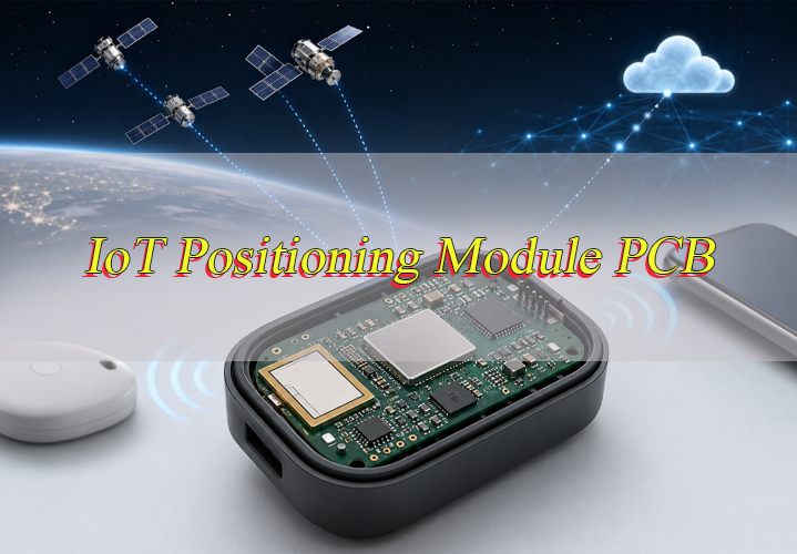
- Improved positioning
- XR, AR, VR, and immersive communication support
- Better industrial IoT support
- Stronger integration with non-terrestrial networks
One practical point is uplink. Many earlier mobile networks were designed around download-heavy traffic, such as video streaming. But collaboration tools, cloud storage, live video, machine vision, AI terminals, and connected vehicles are increasing uplink pressure. This affects radio planning, antenna design, baseband capacity, and backhaul requirements.
5G-Advanced is also important for industrial applications. Factories and automated sites often need predictable connectivity, not just peak speed. Better positioning, lower latency, and more reliable device management can support robots, AGVs, sensors, cameras, and machine control systems.
Why Are Private 5G Networks Growing in Industrial Deployment?
Private 5G networks are growing because many industrial sites need dedicated, controllable, and reliable wireless connectivity.
A private 5G network is built for a specific enterprise, factory, port, mine, logistics center, hospital, campus, or energy facility. It may use local spectrum, shared spectrum, or licensed operator spectrum depending on the country and business model. Unlike public mobile networks, private networks can be optimized around the site’s own machines, traffic, security rules, and coverage requirements.
Private 5G is especially useful where Wi-Fi may struggle with mobility, interference, wide-area coverage, or deterministic performance. It is not always a replacement for Wi-Fi. In many real projects, both technologies work together.
| Network Type | Best Use Case | Strength | Limitation |
|---|---|---|---|
| Wi-Fi | Offices, indoor IT access, low-cost local connectivity | Easy deployment and broad device support | Interference and mobility limits in complex industrial sites |
| Public 5G | Consumer mobile service and wide-area access | Large coverage and operator-managed service | Less customized for one factory or campus |
| Private 5G | Industrial automation, ports, mines, smart factories | Better control, mobility, security, and reliability | Requires planning, spectrum strategy, and integration |
For electronics suppliers, private 5G creates demand for industrial gateways, RF control units, rugged routers, sensor hubs, edge computing modules, camera systems, and automation controllers. These products often work in harsh environments, so PCB design must consider vibration, temperature cycling, electromagnetic interference, thermal stress, and long service life.
How Is Fixed Wireless Access Becoming a Major 5G Deployment Model?
Fixed wireless access is becoming a major 5G deployment model because it can deliver broadband without waiting for fiber to reach every building.
5G FWA uses wireless links to provide home or business internet access. A customer premises equipment unit receives the wireless signal and converts it into local Wi-Fi or wired connectivity. For operators, this can be faster and more flexible than laying new fiber in every location. For users, it can provide a practical broadband option in rural, suburban, temporary, or underserved areas.
FWA is attractive in several scenarios:
- Rural broadband expansion
- Suburban home internet
- Backup connectivity for small businesses
- Temporary construction sites
- Retail branches
- Remote offices
- Areas where fiber installation is slow or expensive
However, FWA has real engineering challenges. The network must handle capacity, indoor coverage, line-of-sight limitations, weather exposure, and customer equipment reliability. Outdoor CPE products need stable RF performance, waterproof housing, antenna integration, heat dissipation, and long-term power stability.
How Will AI-Native Networks Shape 5G Deployment?
AI-native networks will shape 5G deployment by making planning, operation, optimization, and fault management more automated.
Telecom networks are too complex to manage only with manual configuration. A modern 5G network includes many frequency bands, multiple radio layers, cloud infrastructure, edge nodes, user mobility patterns, and enterprise service levels. AI can help operators analyze traffic, predict congestion, detect abnormal behavior, optimize energy usage, and adjust network resources more efficiently.
Common AI applications in 5G networks include:
- Traffic forecasting
- Energy-saving control
- Radio parameter optimization
- Fault prediction
- Anomaly detection
- Customer experience analysis
- Network slicing management
- Capacity planning
- Automated troubleshooting
This does not mean the network runs without engineers. It means engineers get better tools. AI can process large amounts of network data, but deployment still requires careful planning, field validation, and hardware reliability.
How Are Satellite-to-Cellphone and NTN Technologies Affecting 5G Coverage?
Non-terrestrial networks are helping 5G reach areas where traditional terrestrial networks are difficult or expensive to deploy.
NTN can include satellite-based communication, high-altitude platforms, or other non-ground infrastructure. In 5G discussions, satellite-to-cellphone connectivity receives strong attention because it can extend basic coverage to remote regions, oceans, mountains, disaster areas, and emergency scenarios.
This does not mean satellites will replace terrestrial 5G towers. Macro base stations, small cells, and fiber-connected infrastructure remain essential for capacity and low-latency services in cities and industrial areas. NTN is better understood as a complementary layer.
Typical NTN-related use cases include:
- Emergency messaging
- Remote worker communication
- Maritime connectivity
- Aviation connectivity
- Logistics tracking
- Rural and mountain coverage
- Disaster recovery
- Backup connectivity for critical operations
For hardware design, NTN and satellite-related modules raise demanding RF requirements. Products may need compact antenna systems, low-noise front-end design, reliable frequency stability, thermal control, and careful shielding. In compact devices, board layout becomes even more sensitive because space is limited and RF performance must remain stable.
What Spectrum Trends Are Influencing 5G Network Deployment?
Spectrum strategy directly affects 5G coverage, capacity, cost, and hardware design.
Low-band spectrum gives better coverage and building penetration, but lower capacity. Mid-band spectrum, especially C-band in many markets, provides a strong balance between coverage and capacity. mmWave offers very high capacity, but its coverage distance and penetration are limited, so it works best in dense urban hotspots, stadiums, transport hubs, and fixed wireless access scenarios.
| Spectrum Type | Coverage | Capacity | Common Use Case | Hardware Challenge |
|---|---|---|---|---|
| Low-band | Wide coverage | Lower capacity | Rural coverage, nationwide service | Antenna size and spectrum efficiency |
| Mid-band | Balanced coverage | High capacity | Urban and suburban 5G | RF linearity, power efficiency, MIMO complexity |
| C-band | Strong mid-band option | High capacity | Main 5G capacity layer | Thermal design and base station density |
| mmWave | Shorter range | Very high capacity | Hotspots, FWA, venues | Signal loss, antenna integration, PCB material loss |
| Private spectrum | Site-specific | Depends on band | Factory, port, campus | Local planning and industrial equipment support |
Spectrum choices influence base station architecture, antenna design, RF power levels, filtering, PCB substrate choice, and thermal management. A product designed for low-band infrastructure will not face the same board-level challenges as a mmWave antenna module or high-capacity active antenna unit.
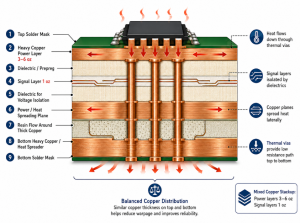
What Hardware Challenges Come with 2026 5G Deployment?
The biggest hardware challenges in 2026 5G deployment are RF loss, signal integrity, heat, power density, miniaturization, and reliability.
Telecom equipment is expected to operate continuously. Outdoor base station equipment may face temperature variation, humidity, vibration, dust, and power fluctuation. Indoor edge devices may be compact but still need high throughput and stable thermal performance. Industrial 5G devices may operate near motors, inverters, robotic systems, or high-current equipment, where electromagnetic noise can affect performance.
Important hardware challenges include:
- High-frequency signal loss
- Controlled impedance stability
- Crosstalk between high-speed lines
- RF path consistency
- Antenna feed accuracy
- Power amplifier heat
- BGA solder joint reliability
- Thermal cycling stress
- EMI and shielding performance
- Long-term material stability
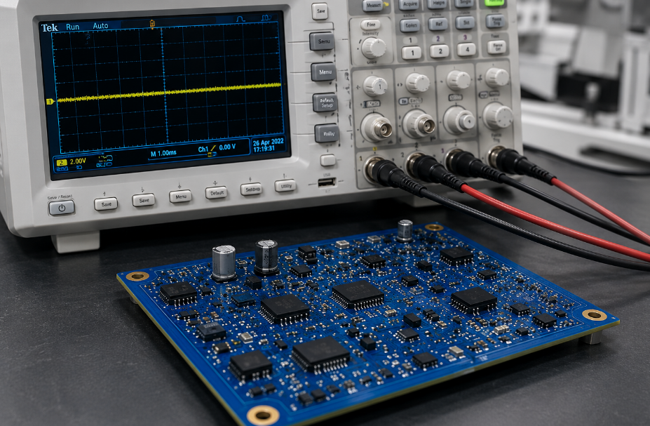
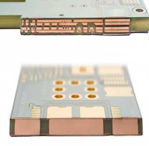
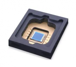
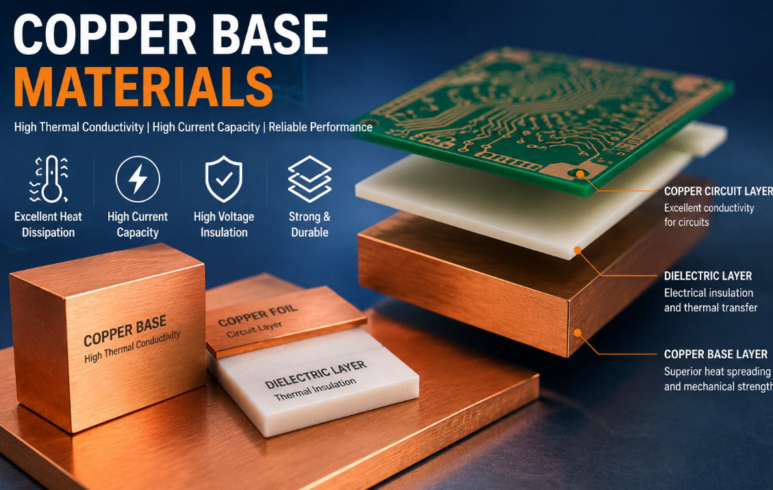
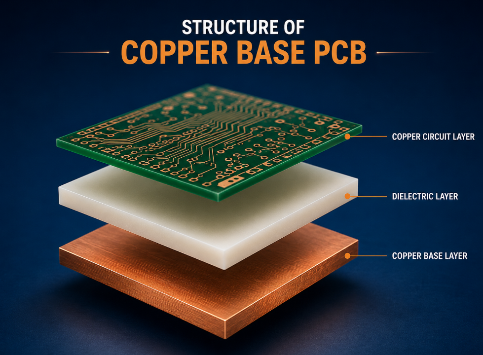
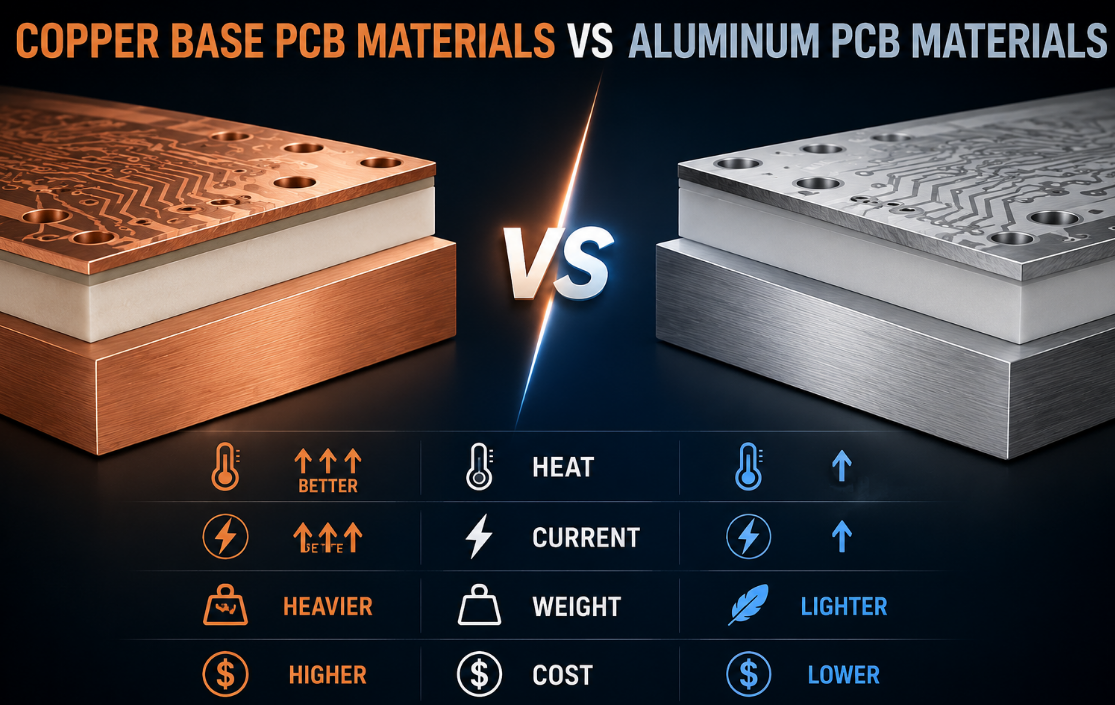
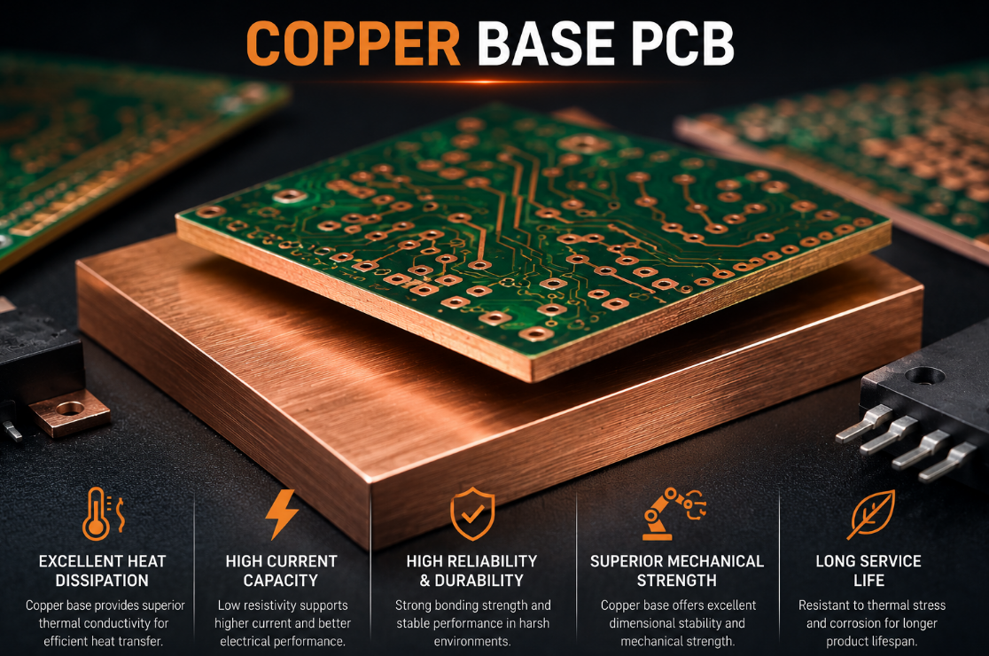
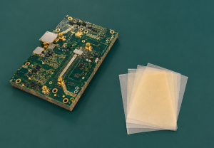
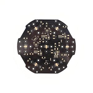
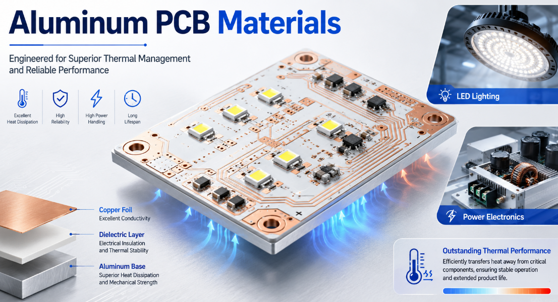
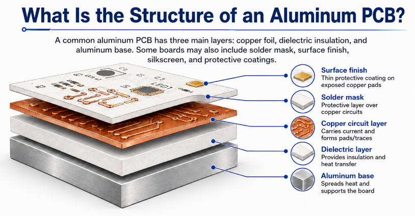
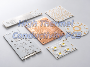
This is where PCB and PCBA decisions become important. High-frequency PCB materials may be needed for RF paths. High-speed PCB stack-ups may be required for baseband, switching, and edge computing hardware. HDI PCB supports compact routing and high-density components. Ceramic PCB and metal core PCB may be useful where heat dissipation is critical. Impedance control is essential when signals move at high speeds or when RF performance must be predictable.
A 5G product can fail not because the system architecture is wrong, but because the physical implementation is weak. Poor stack-up design, unstable dielectric properties, plating defects, bad via transitions, weak solder joints, or insufficient thermal paths can reduce performance and reliability.
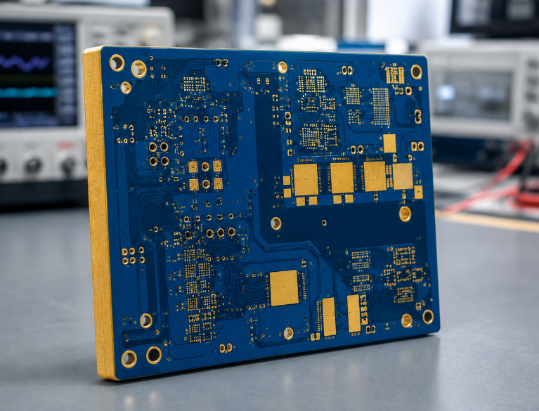
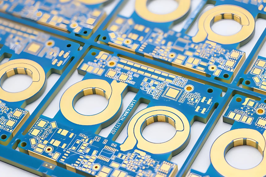
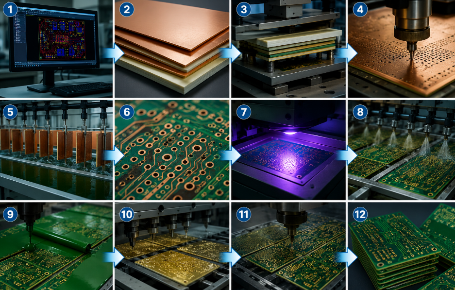
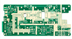
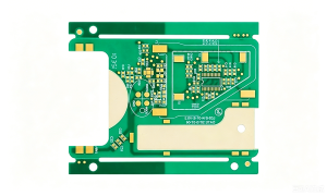
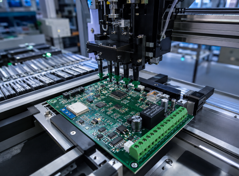
What Does 5G Deployment Mean for PCB and PCBA Manufacturing?
5G deployment means PCB and PCBA manufacturing must support higher technical requirements and tighter process control.
Telecom equipment covers many product types. Each one has different board requirements.
| Product Type | Typical PCB/PCBA Requirement | Key Manufacturing Concern |
|---|---|---|
| Base station board | High-speed signal routing, power stability | Impedance control, layer stack-up, via reliability |
| RF front-end module | Low-loss signal path, shielding | High-frequency material, copper roughness, RF layout |
| Antenna board | Stable RF feed and compact design | Material consistency, dimensional accuracy |
| Edge computing module | High-speed data and heat control | BGA assembly, thermal management, power integrity |
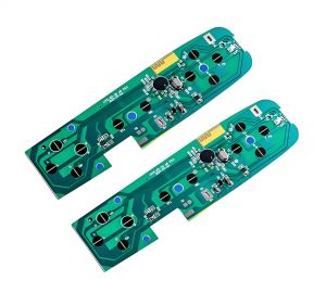
| 5G router/CPE | RF, digital, power, and antenna integration | DFM review, EMI control, compact PCBA assembly |
| Industrial gateway | Rugged operation and long life | Component selection, conformal coating, testing |
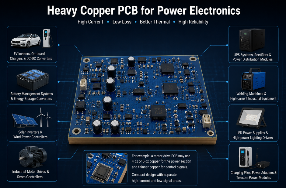
| Power amplifier board | High heat and stable current delivery | Copper thickness, thermal vias, substrate selection |
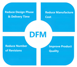
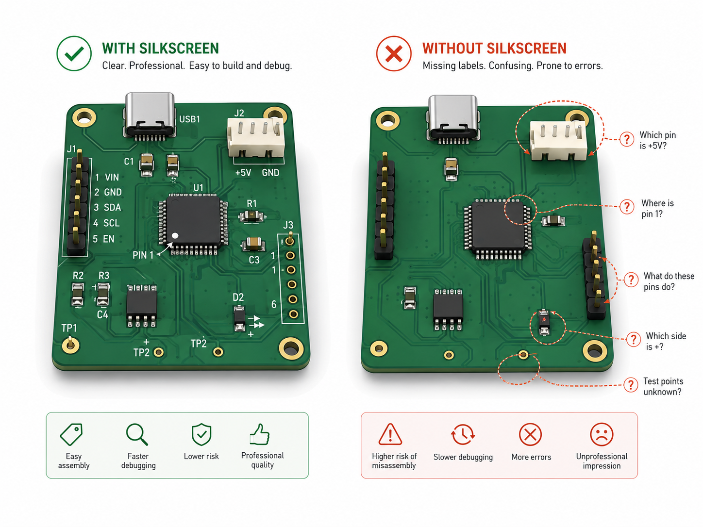
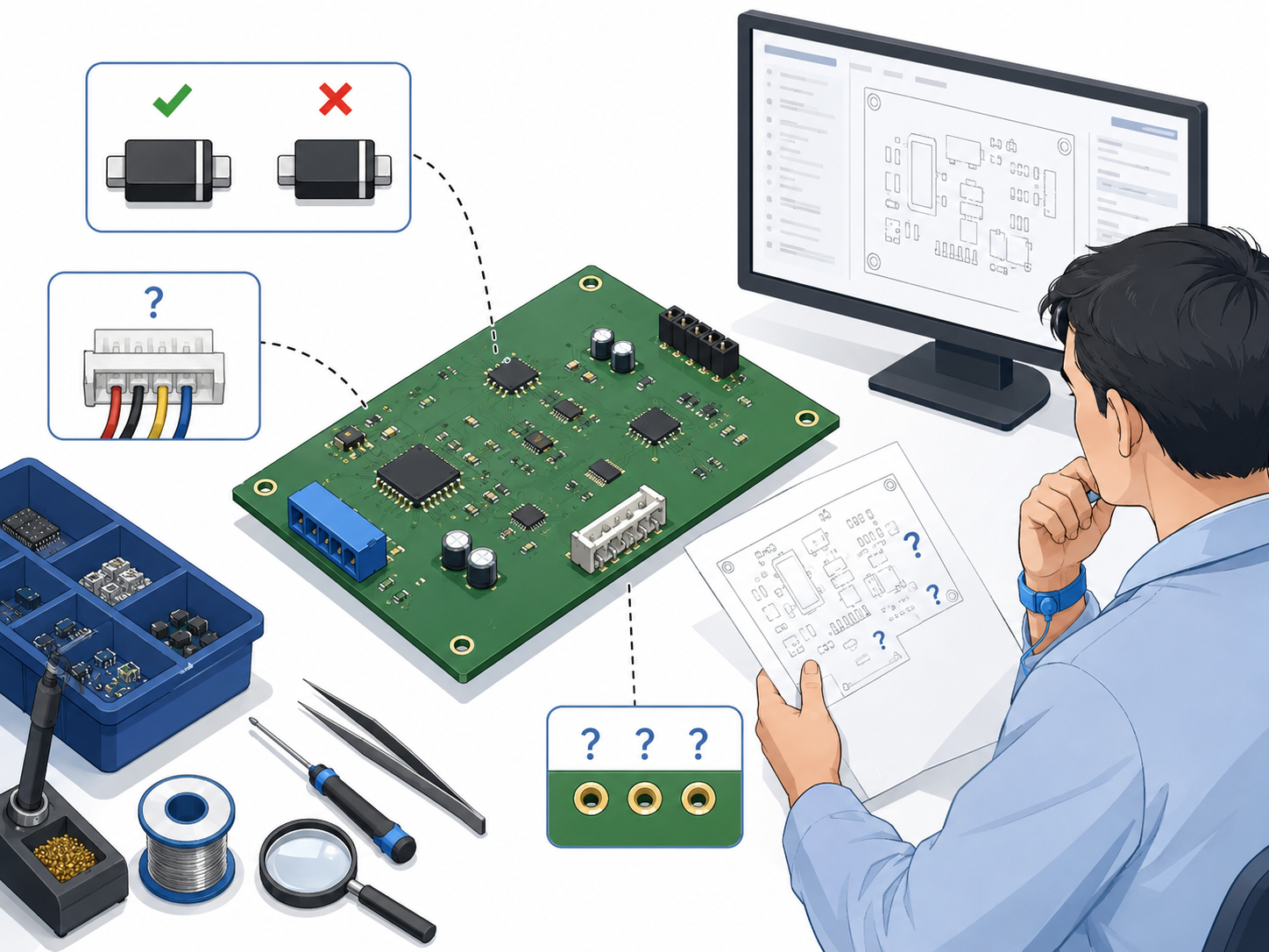
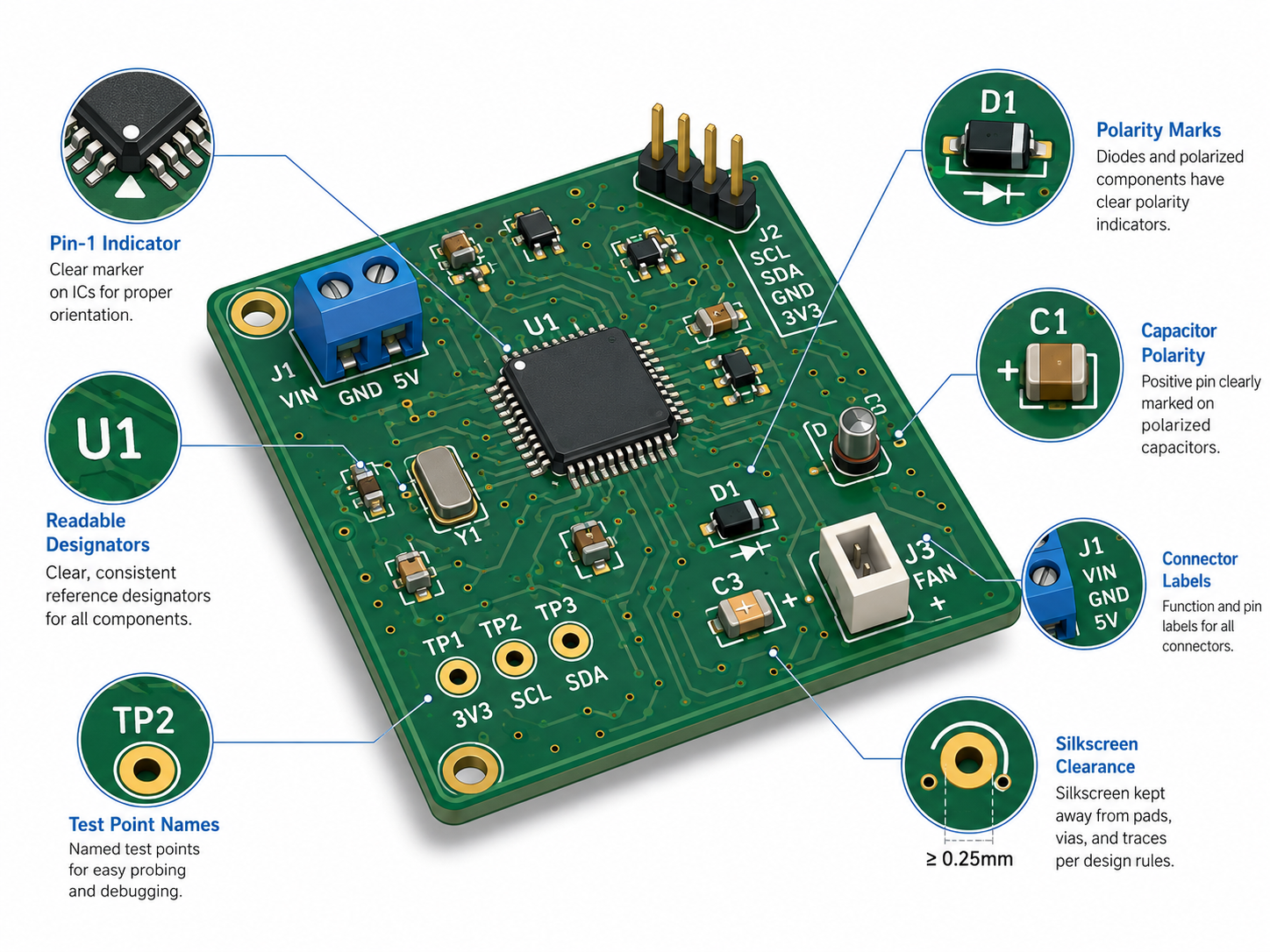
Manufacturing checks should start before production. For 5G-related boards, engineering teams should review:
- Gerber files
- Stack-up design
- Controlled impedance requirements
- RF material specification
- Copper thickness
- Surface finish
- Via structure
- BGA package requirements
- Thermal design
- Solder mask clearance
- Assembly process
- AOI, X-ray, ICT, and functional test requirements
The more advanced the 5G application, the earlier manufacturability should be reviewed. For example, a high-speed edge computing board may need careful via back-drilling, differential pair control, power plane planning, and thermal relief design. A high-frequency antenna board may need stable dielectric constant, low dissipation factor, precise etching, and strict handling during fabrication.
What Are the Main 5G Deployment Challenges in 2026?
The main 5G deployment challenges in 2026 are cost, complexity, energy consumption, spectrum planning, site access, security, and hardware reliability.
Even when the technology is ready, deployment can still be difficult. Operators must balance investment with service revenue. Enterprises must decide whether private 5G is necessary or whether Wi-Fi, wired Ethernet, or public 5G can meet their needs. Equipment manufacturers must deliver products that are reliable, efficient, and cost-controlled.
Major challenges include:
- High infrastructure investment
- SA core migration complexity
- Spectrum availability and auction cost
- Site acquisition and permitting
- Backhaul capacity
- Energy consumption
- Device ecosystem maturity
- Multi-vendor integration
- Cybersecurity requirements
- Industrial reliability expectations
- Supply chain stability
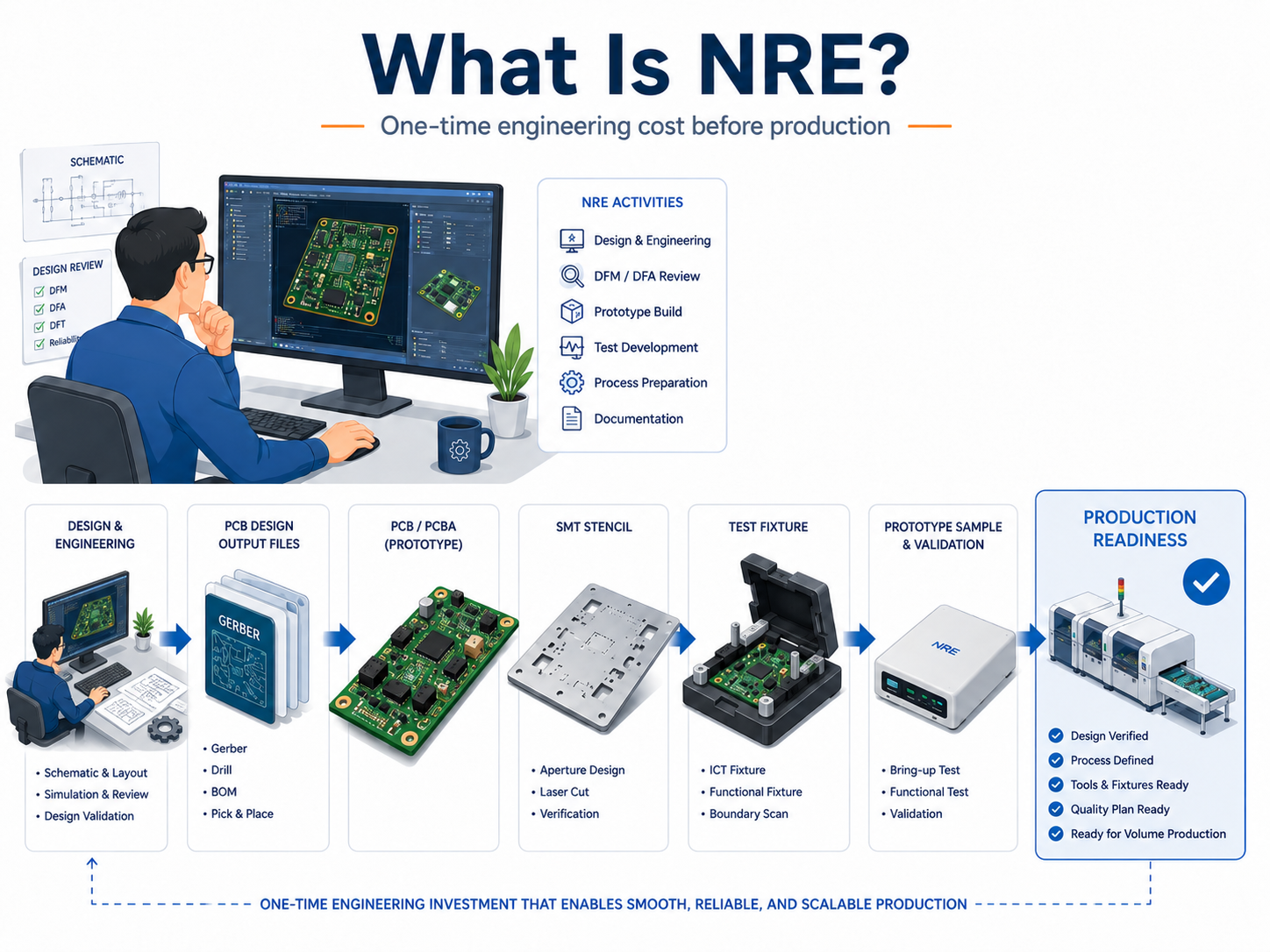
How Should Companies Prepare for 5G Network Deployment Projects?
Companies should prepare for 5G deployment by defining the application goal before selecting the network architecture or hardware platform.
For hardware buyers and product developers, preparation should include a clear technical file package:
- Gerber files
- BOM
- Pick-and-place file
- Stack-up requirements
- Controlled impedance values
- RF material requirements
- Operating frequency range
- Thermal requirements
- Environmental requirements
- Expected test methods
- Production quantity
- Application scenario
For PCB/PCBA sourcing, buyers should choose suppliers with experience in high-frequency PCB, high-speed PCB, impedance control, HDI structures, thermal materials, and telecom-grade assembly. The supplier should be able to review manufacturability before production, not only quote a price from the file package.
What Are the Key 5G Network Deployment Trends to Watch After 2026?
After 2026, 5G deployment will continue moving toward intelligence, specialization, and service-based business models.
The main trends to watch include:
- Wider adoption of 5G Standalone
- More commercial network slicing services
- Large-scale 5G-Advanced deployment
- Stronger private 5G growth in industrial markets
- More FWA service packages
- AI-native network operations
- Non-terrestrial network expansion
- More edge computing integration
- More uplink-heavy traffic from AI and cloud applications
- Early 6G research influencing long-term planning
The transition will not happen evenly everywhere. Some regions will focus on 5G SA and advanced enterprise services. Others will focus on broadband coverage and FWA. Some industrial markets will adopt private networks quickly, while smaller businesses may continue using Wi-Fi and public mobile services.
For telecom equipment and electronics suppliers, the direction is clear. Future 5G hardware must be smaller, faster, more power-efficient, more thermally stable, and more reliable. The PCB inside the product will play a direct role in whether the device can meet these expectations.
Key 5G Network Deployment Trends in 2026
| Trend | What It Means | Main Benefit | Deployment Challenge | Hardware Impact |
|---|---|---|---|---|
| 5G Standalone | 5G network with dedicated 5G core | Better slicing, latency, and enterprise services | Core migration and service orchestration | More demand for edge and core network hardware |
| 5G-Advanced | Evolution of 5G through advanced releases | Better performance, efficiency, and automation | Network and device readiness | Higher RF and signal integrity requirements |
| Private 5G | Dedicated enterprise network | Security, reliability, and local control | Spectrum and integration planning | Industrial gateways and rugged PCBA |
| FWA | Broadband through wireless access | Faster broadband rollout | Capacity and indoor signal quality | RF modules, antennas, and thermal design |
| Open RAN | More open multi-vendor RAN architecture | Vendor flexibility and software innovation | Interoperability and power efficiency | Modular radio and compute hardware |
| AI-Native Network | AI-assisted planning and operation | Efficiency and automation | Data quality and model reliability | Edge compute and high-speed PCB demand |
| NTN | Satellite-supported connectivity | Remote and emergency coverage | Cost, latency, and device support | Satellite RF modules and compact antenna boards |
FAQs
What is the difference between 5G NSA and 5G SA?
5G NSA uses 5G radio access with an existing 4G core network. It helps operators launch faster but limits some advanced features. 5G SA uses a dedicated 5G core, which supports better latency, network slicing, cloud-native services, and enterprise applications. SA is more complex to deploy, but it gives operators more long-term service flexibility.
Why is 5G Standalone important for future networks?
5G Standalone is important because it unlocks more of the original 5G design. It allows operators to build services around slicing, low latency, automation, and enterprise-grade connectivity. Without SA, many advanced use cases remain limited. For industrial users, SA can support more predictable performance, better security control, and more flexible network management.
What is 5G-Advanced?
5G-Advanced is the next evolution of 5G, starting with 3GPP Release 18 and continuing in later releases. It improves performance, energy efficiency, positioning, mobility, AI support, XR services, industrial applications, and non-terrestrial network integration. It is not a completely new generation, but it makes current 5G networks more capable and intelligent.
Is 5G-Advanced the same as 6G?
No. 5G-Advanced is still part of the 5G family. It improves current 5G systems and prepares the industry for future network functions. 6G will be a new generation with new specifications, commercial models, and technical targets. In practical deployment, 5G-Advanced acts as a bridge between today’s 5G and future 6G systems.
Why are private 5G networks growing?
Private 5G networks are growing because industrial users need wireless connectivity that is reliable, secure, and controllable. Factories, ports, mines, campuses, and logistics centers often need better mobility and coverage than traditional Wi-Fi can provide in difficult environments. Private 5G can be customized for machines, cameras, sensors, robots, and local data policies.
What industries benefit most from private 5G?
Manufacturing, logistics, ports, mining, energy, healthcare, education, and smart campuses can benefit from private 5G. These industries often need stable wireless communication across large spaces or complex environments. Private 5G is especially useful when devices are moving, data must stay local, or the site needs predictable latency and strong security controls.
How does 5G FWA work?
5G FWA delivers broadband through a wireless 5G connection instead of a fixed fiber line to the building. A customer device receives the 5G signal and provides internet access through Wi-Fi or Ethernet. It can help operators expand broadband faster in rural, suburban, or temporary locations, especially where fiber installation is slow or expensive.
Conclusion
PCB and PCBA quality will become more important as 5G equipment becomes smaller, faster, and more integrated. High-frequency materials, controlled impedance, HDI structures, thermal substrates, stable assembly, and strict testing all help telecom products perform reliably in real deployment environments.
If you’re sourcing reliable PCB/PCBA manufacturing — OEM, ODM, prototyping, mass production, or custom engineering solutions — reach out to our engineering team for technical support and a quote at sales@bestpcbs.com.