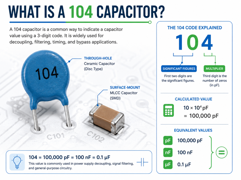
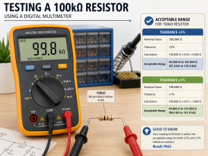
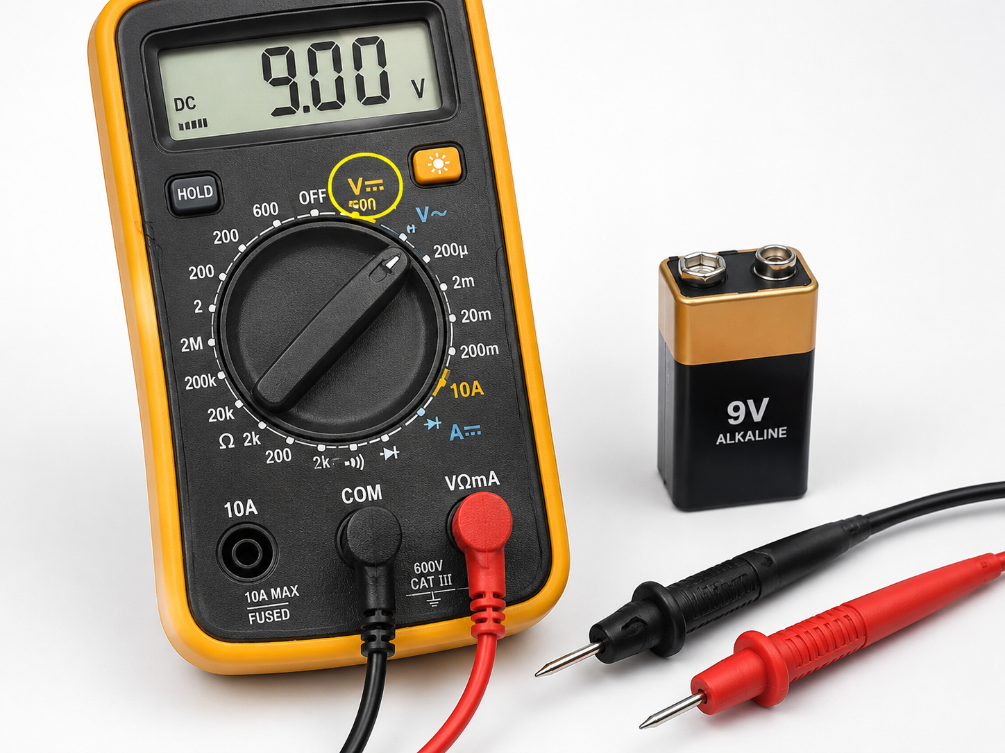
The DC voltage symbol is one of the most common markings you will see on a multimeter, power adapter, battery label, circuit diagram, or PCB-related test document. It helps you identify direct current voltage, which flows in one stable direction. For anyone working with electronics, power supplies, batteries, LED modules, automotive circuits, or PCB assemblies, understanding this symbol is basic but important.
Many users search for the dc voltage symbol on multimeter because the markings can look confusing at first. Some meters use “V⎓,” some use “VDC,” and others show a solid line above a dashed line. Once you know what these symbols mean, it becomes much easier to choose the correct setting, measure voltage safely, and avoid damaging a circuit or device.
What Is Symbol for DC Voltage?
The most common DC voltage symbol is:
V⎓
This symbol usually means DC volts. The “V” stands for voltage, while the straight line and dashed line represent direct current. In many multimeters, the DC voltage function may also appear as:
| DC Voltage Marking | Meaning |
|---|---|
| V⎓ | DC voltage |
| VDC | Volts direct current |
| DCV | Direct current voltage |
| V with straight/dashed line | DC voltage measurement mode |
The straight line indicates a steady voltage level. The dashed line under it suggests the reference line or lower potential. Together, they identify voltage that flows in one direction.
You will often see this symbol when measuring batteries, DC power supplies, solar panels, USB power outputs, automotive circuits, LED drivers, and PCB power rails. For example, a 5V USB port, a 12V battery, and a 24V industrial control power supply are all common DC voltage sources.
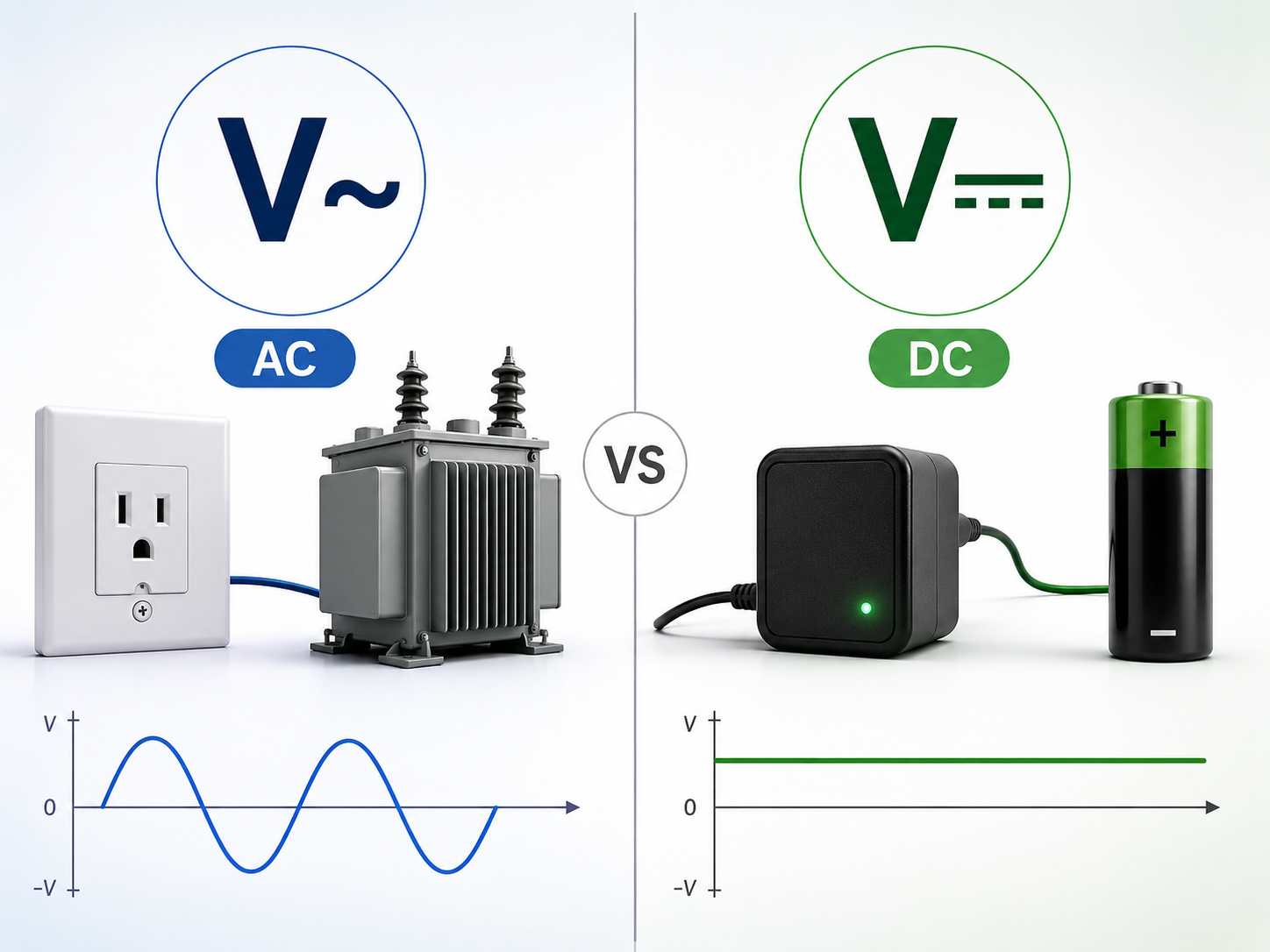
AC vs DC Voltage Symbol
AC and DC voltage symbols are different because they represent different types of electrical behavior. AC means alternating current, where the voltage changes direction periodically. DC means direct current, where voltage polarity stays consistent.
| Type | Common Symbol | Common Marking | Typical Source |
|---|---|---|---|
| AC voltage | V~ | VAC / ACV | Wall outlet, transformer output |
| DC voltage | V⎓ | VDC / DCV | Battery, adapter, PCB power rail |
| AC/DC combined | V~ / V⎓ | Auto voltage mode | Auto-ranging multimeters |
The AC voltage symbol is usually shown as a wavy line: ~. This represents a waveform that alternates over time. The DC voltage symbol uses a straight line with a dashed line, showing a more stable voltage direction.
For simple identification:
- V~ means AC voltage.
- V⎓ means DC voltage.
- A~ means AC current.
- A⎓ means DC current.
This distinction matters during testing. Measuring a DC circuit in AC mode may give an unstable or misleading reading. Measuring an AC source in DC mode may show zero, a fluctuating number, or a value that does not explain the real voltage condition.
What Is DC Voltage Range?
DC voltage range refers to the maximum DC voltage level a multimeter can measure under a selected setting. On manual-range multimeters, you may see settings such as:
| Range | Suitable Use |
|---|---|
| 200mV DC | Small sensor signals, low-level circuits |
| 2V DC | Small batteries, logic signals |
| 20V DC | 1.5V, 3.3V, 5V, 9V, 12V circuits |
| 200V DC | Higher DC systems |
| 600V / 1000V DC | High-voltage DC systems, depending on meter rating |
For most PCB and electronic product testing, the 20V DC range is commonly used because many circuits operate at 1.8V, 3.3V, 5V, 9V, or 12V. Industrial control boards may also use 24V DC input.
If your multimeter is auto-ranging, you usually only need to select the DC voltage mode. The meter will choose the correct range by itself. If your meter is manual-ranging and you are not sure about the voltage level, start with a higher range, then move down for better resolution.
For example, when measuring an unknown DC source, do not start at 2V. Start at 200V or the highest suitable range, then reduce the range after you confirm the voltage is safe for the meter.
DC Voltage Symbol in Multimeter
The dc voltage symbol in multimeter is usually placed around the rotary dial. Depending on the model, it may appear beside the voltage setting or within a shared voltage section.
Common markings include:
| Multimeter Symbol | Meaning |
|---|---|
| V⎓ | Measure DC voltage |
| V~ | Measure AC voltage |
| mV⎓ | Measure small DC voltage |
| AUTO V | Auto-detect AC/DC voltage on some meters |
| VΩHz | Input jack for voltage, resistance, and frequency |
Most digital multimeters have three main ports:
| Port | Use |
|---|---|
| COM | Black probe, common reference |
| VΩ | Red probe for voltage, resistance, diode, continuity |
| A / mA / μA | Red probe for current measurement |
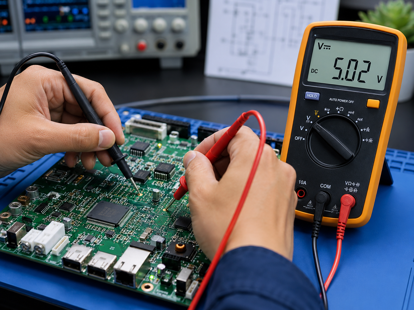
For DC voltage measurement, the black probe normally goes into COM, and the red probe goes into the VΩ port. The red probe touches the positive side of the circuit, and the black probe touches ground or the negative side.
If the probes are reversed during DC measurement, the meter usually shows a negative value. For example, a 12V battery may display -12.00V. This does not mean the battery is damaged. It only means the probe polarity is reversed.
How to Use DC Symbol on Multimeter?
To use the DC voltage function on a multimeter, follow these steps:
- Insert the black probe into the COM port.
- Insert the red probe into the VΩ port.
- Turn the dial to the V⎓, VDC, or DCV setting.
- Choose a proper voltage range if your meter is manual-ranging.
- Place the black probe on the negative side or ground.
- Place the red probe on the positive test point.
- Read the voltage value on the display.
For a simple battery test, touch the black probe to the negative terminal and the red probe to the positive terminal. A healthy AA battery may read around 1.5V when new. A typical car battery may read around 12.6V when fully charged and at rest.
For PCB testing, you may measure between a power rail and ground. For example:
| Circuit Point | Expected Reading |
|---|---|
| 5V rail to GND | Around 5V DC |
| 3.3V rail to GND | Around 3.3V DC |
| 12V input to GND | Around 12V DC |
| 24V input to GND | Around 24V DC |
Do not let the probe tips slip and short two pins together. On dense PCB assemblies, a probe slip can damage components, burn a trace, or shut down the board. Fine probe tips or grabber clips are safer for compact test points.
Is 12 Volt AC or DC?
12 volt can be AC or DC. The voltage number alone does not tell you the current type. You need to check the label, symbol, source, or application.
A 12V battery is DC. A 12V adapter may be DC if its label shows 12V⎓ or 12V DC. A transformer output may be 12V AC if the label shows 12V~ or 12V AC.
| Label | Meaning |
|---|---|
| 12V DC | 12 volts direct current |
| 12V⎓ | 12 volts DC |
| 12V AC | 12 volts alternating current |
| 12V~ | 12 volts AC |
This point is especially important for LED strips, CCTV cameras, routers, control boards, and small electronic modules. Many of these devices require 12V DC. Supplying 12V AC to a device designed for 12V DC may cause overheating or component failure.
How to Tell If Voltage Is AC or DC?
You can identify AC or DC voltage by checking four things: the symbol, the label, the source, and the multimeter reading.
The easiest method is to read the power label. If it shows V⎓, DC, or VDC, it is DC. If it shows V~, AC, or VAC, it is AC.
You can also judge by the source:
| Source | Usually AC or DC? |
|---|---|
| Wall outlet | AC |
| Battery | DC |
| USB charger output | DC |
| Solar panel output | DC |
| Laptop adapter output | DC |
| Doorbell transformer | Often AC |
| PCB power rail | Usually DC |
A multimeter can confirm this. Set the meter to AC voltage first if the source is unknown and could be connected to mains or transformer power. Then test in DC mode if needed. For low-voltage electronics, DC mode is often the correct setting, but you should still read the label before connecting anything.
On PCB assemblies, power input markings such as VIN, VCC, GND, +12V, +5V, and +3V3 usually indicate DC rails. AC input areas may be marked L, N, AC IN, or VAC.
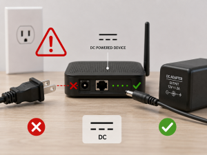
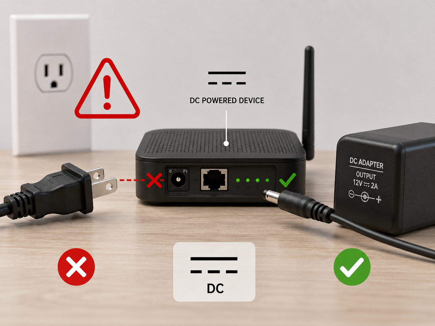
What Happens If I Plug AC into DC?
Plugging AC into a DC device can cause serious problems. The result depends on the circuit design, voltage level, protection components, and how long the wrong power is applied.
Possible outcomes include:
| Situation | Possible Result |
|---|---|
| AC connected to a DC-only device | Overheating, unstable operation, component failure |
| Wrong polarity DC connected | Protection diode may conduct, fuse may blow, circuit may fail |
| AC voltage too high | Regulator, capacitor, IC, or PCB trace damage |
| Short exposure with protection | Device may survive, but inspection is still needed |
Many DC devices use electrolytic capacitors, voltage regulators, ICs, and protection circuits designed for fixed polarity. AC reverses polarity repeatedly, so those parts may be stressed beyond their rating.
Some devices include a bridge rectifier, fuse, TVS diode, or reverse-polarity protection. These features improve tolerance, but they do not make every DC device safe for AC input. Always match the adapter output type with the device input requirement.
For PCB and PCBA projects, this is one reason input protection design matters. Clear silkscreen markings, proper connector selection, fuse protection, reverse-polarity protection, and correct capacitor voltage ratings can reduce field failures.
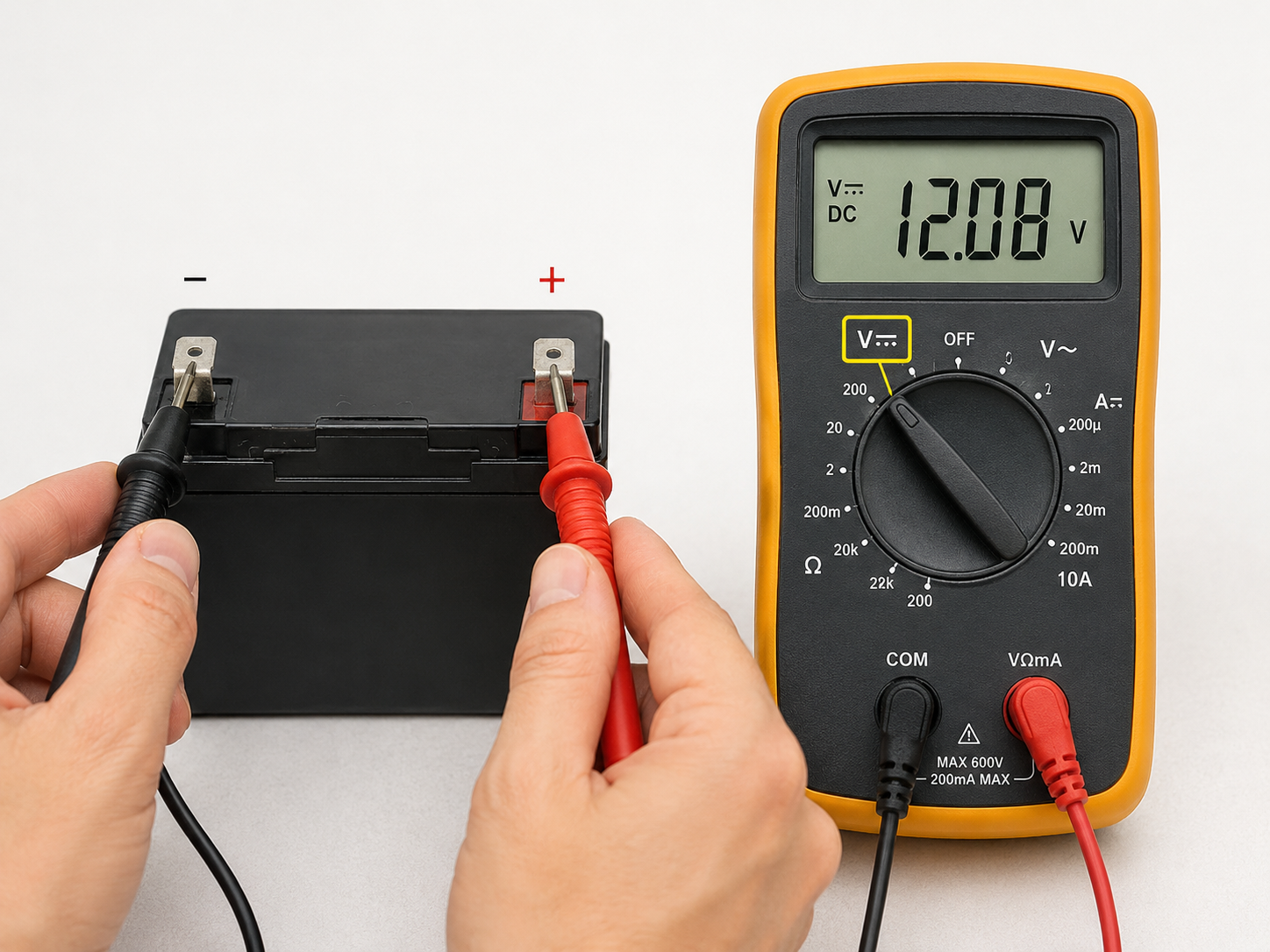
How to Read DC Volts?
To read DC volts correctly, you need to understand the displayed number and polarity.
If your meter shows:
12.08V
It means the voltage difference between the red probe and black probe is 12.08 volts DC. If the display shows:
-12.08V
The voltage magnitude is still about 12.08 volts, but the red probe is connected to the lower-potential point and the black probe is connected to the higher-potential point.
For electronic circuits, common DC voltage readings include:
| Reading | Common Meaning |
|---|---|
| 1.5V | AA/AAA battery, small sensor supply |
| 3.3V | MCU, logic IC, communication module |
| 5V | USB, logic circuit, relay module |
| 9V | Small battery-powered equipment |
| 12V | LED strip, automotive accessory, adapter output |
| 24V | Industrial control, PLC input, motor control |
A small difference from the rated voltage is normal. For example, a 5V rail may read 4.98V or 5.05V. Whether this is acceptable depends on the tolerance of the powered circuit.
When measuring on a PCB, choose a stable ground point. Avoid using random metal parts unless you know they are connected to the circuit ground. For switching power supplies, motor drivers, and high-current boards, ground layout can affect readings. A voltage measured at the connector may be slightly different from the voltage measured near the load.
What Does DC in 24V Mean?
DC in 24V means the voltage is 24 volts direct current. The polarity remains fixed: one side is positive, and the other side is negative or ground.
24V DC is common in industrial electronics, automation equipment, control panels, sensors, relays, LED systems, and some motor control applications. It is popular because it offers better noise margin than 5V or 12V systems and is still safer and easier to handle than many high-voltage systems.
On a product label, you may see:
Input: 24V⎓ 2A
This means the device requires a 24V DC power supply capable of providing up to 2A. The adapter must match both voltage and current requirements. A power supply with the correct voltage and a higher current capacity is usually acceptable, because the device draws only what it needs. A supply with the wrong voltage type is not acceptable.
For example:
| Device Requirement | Correct Supply? | Reason |
|---|---|---|
| 24V DC, 2A | 24V DC, 3A | Yes, voltage matches and current capacity is enough |
| 24V DC, 2A | 24V DC, 1A | Not ideal, current capacity is too low |
| 24V DC, 2A | 24V AC, 2A | No, voltage type is wrong |
| 24V DC, 2A | 12V DC, 2A | No, voltage is too low |
Common Places Where You See the DC Voltage Symbol
The dc voltage symbol is not limited to multimeters. It also appears on many everyday and industrial products.
| Place | Example |
|---|---|
| Power adapter label | Output: 12V⎓ 1A |
| Battery charger | DC output rating |
| PCB silkscreen | +5V, +12V, GND |
| Product manual | Input voltage requirement |
| Test procedure | Measure VDC at TP1 |
| Multimeter dial | V⎓ setting |
| Power supply panel | DC output terminal |
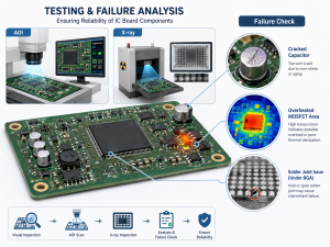
In PCB manufacturing and assembly, DC voltage markings are often used during functional testing. Test engineers may check whether each power rail is within tolerance before moving to signal testing. A board with wrong DC voltage may fail boot-up, reset repeatedly, heat up, or damage downstream ICs.
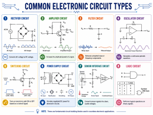
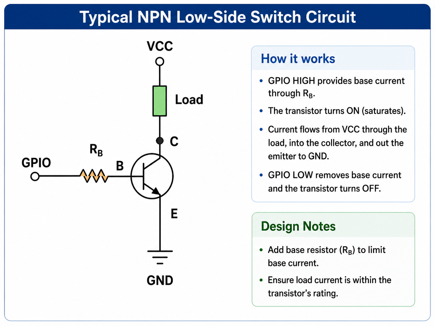
DC Voltage Symbol on Circuit Diagrams
In circuit diagrams, DC voltage may be shown through labels rather than a special symbol. Common labels include:
| Circuit Label | Meaning |
|---|---|
| VCC | Positive supply voltage, often for IC circuits |
| VDD | Positive supply, often used in MOS/CMOS circuits |
| VIN | Voltage input |
| VBAT | Battery voltage |
| GND | Ground reference |
| +5V / +3.3V / +12V | Named DC power rails |
A schematic may also use a battery symbol, DC source symbol, or power net label. The exact notation depends on the design software and engineering convention.
Why the DC Voltage Symbol Matters in PCB and PCBA Testing?
In PCB and PCBA work, voltage testing is not just a basic operation. It helps confirm whether the board is safe to power, whether regulators work, and whether the assembly matches the design.
Typical DC voltage checks include:
| Test Item | Purpose |
|---|---|
| Input voltage check | Confirm correct power source |
| Regulator output check | Verify 5V, 3.3V, 1.8V, or other rails |
| Battery charging voltage | Confirm charging circuit behavior |
| LED driver output | Check driver voltage range |
| Sensor supply voltage | Ensure stable sensor operation |
| Motor driver supply | Verify high-current DC input |
Correct use of the dc voltage multimeter symbol helps avoid incorrect readings. It also helps technicians separate power problems from soldering defects, component errors, or firmware issues.
For example, if a board does not start, measuring the DC input and regulator output can quickly narrow the issue. If the input is correct but the 3.3V rail is missing, the fault may be around the regulator, enable pin, solder joint, or shorted load.
FAQs About DC Voltage Symbol
Q1: What is the symbol for DC voltage on a multimeter?
The common symbol is V⎓. Some meters use VDC or DCV. These markings all refer to DC voltage measurement.
Q2: What is the difference between V~ and V⎓?
V~ means AC voltage. V⎓ means DC voltage. AC voltage alternates direction, while DC voltage keeps fixed polarity.
Q3: Which multimeter setting should I use for a battery?
Use the DC voltage setting, usually marked as V⎓, VDC, or DCV. Batteries provide direct current voltage.
Q4: Why does my multimeter show a negative DC voltage?
A negative reading usually means the probes are reversed. The red probe is touching the lower-potential side, and the black probe is touching the higher-potential side.
Q5: Can I measure AC voltage with the DC setting?
You should not rely on DC mode for AC voltage. The reading may be zero, unstable, or misleading. Use the V~ setting for AC voltage.
Q6: What does 5V DC mean?
5V DC means five volts direct current. It is common in USB power, logic circuits, microcontrollers, and many PCB assemblies.
Q7: Is 24V DC dangerous?
24V DC is generally considered low voltage, but it can still cause sparks, heating, or circuit damage in high-current systems. Use proper probes, insulation, and power ratings.
Q8: How do I know if my adapter output is AC or DC?
Check the label. V⎓, DC, or VDC means DC output. V~, AC, or VAC means AC output.
Q9: What happens if I use the wrong voltage type?
Using AC where DC is required, or DC where AC is required, may damage the device. The result depends on the circuit protection and voltage level.
Q10: What DC voltage range should I choose on a manual multimeter?
Choose a range higher than the expected voltage. For a 12V circuit, the 20V DC range is usually suitable. For unknown voltage, start higher and reduce the range after confirming the level.