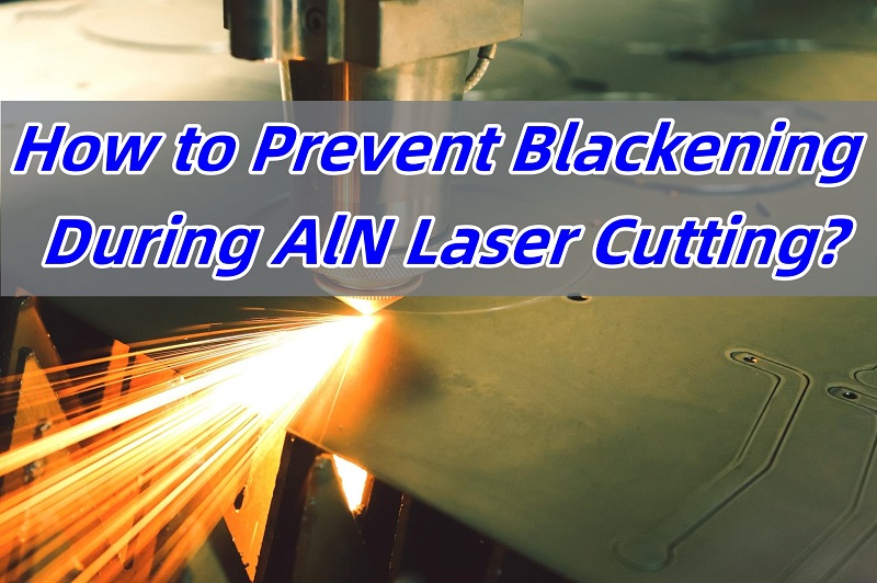
Blackening during AlN laser cutting is a challenge that many engineers and manufacturers face when working with aluminum nitride (AlN) materials. This discoloration can affect both the appearance and performance of the final product, making it crucial to understand the causes and methods to prevent it. In this article, we will explore what AlN laser cutting involves, where it’s commonly used, and the various factors that contribute to blackening. We’ll also offer practical tips for reducing blackening and improving cutting quality.
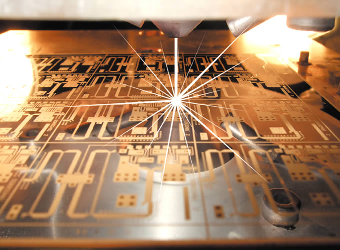
What Is AlN Laser Cutting?
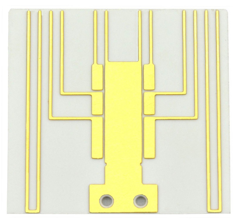
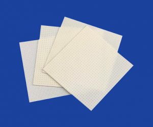
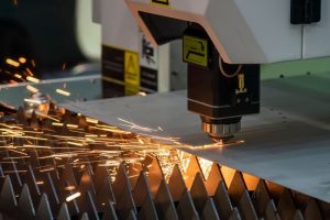
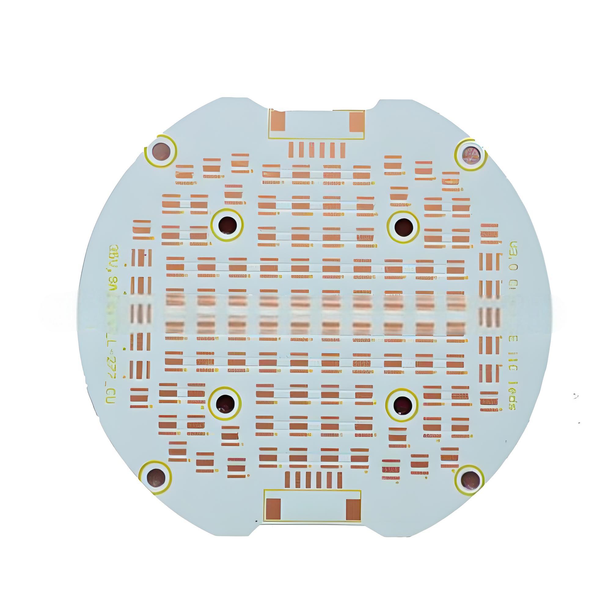
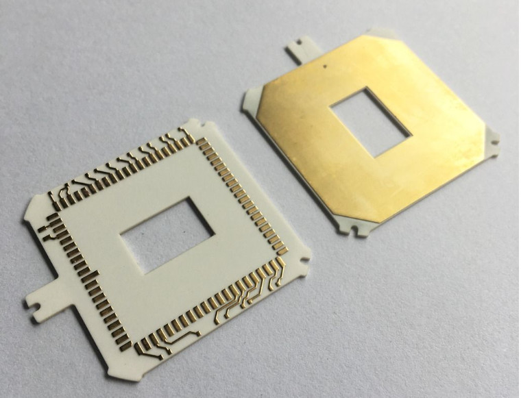
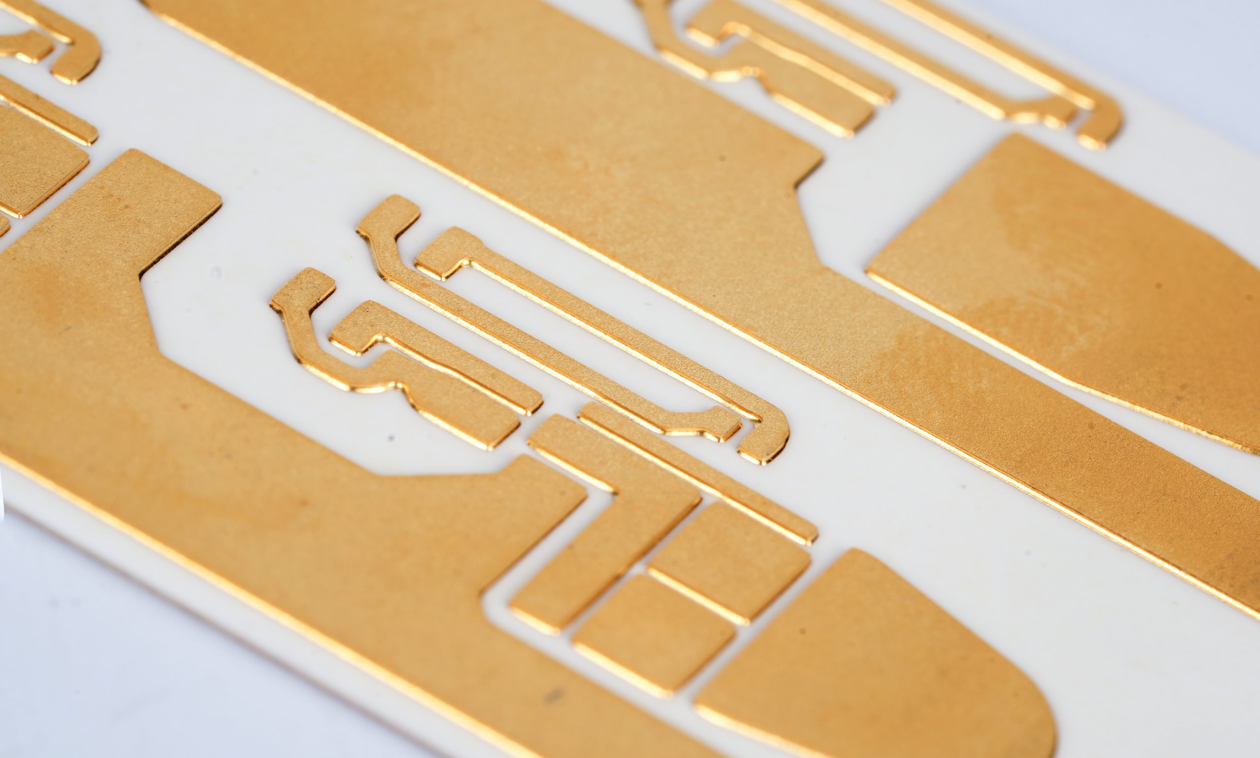
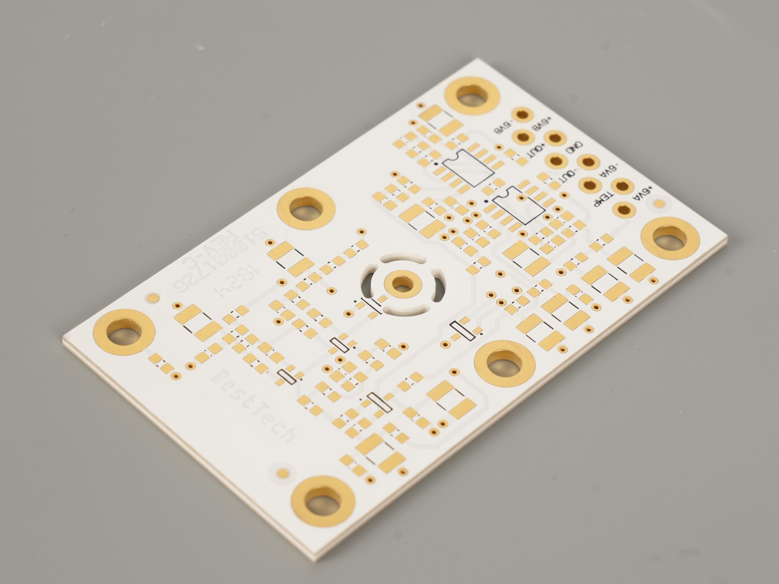
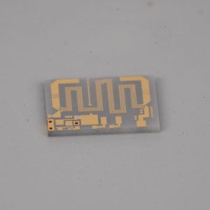
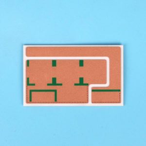
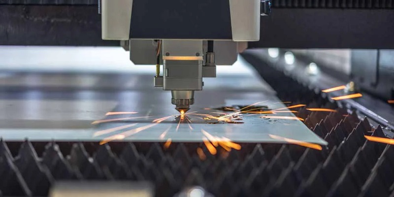
AlN laser cutting is a precise method used to shape and trim aluminum nitride, a ceramic material known for its excellent thermal conductivity and electrical insulation properties. This technique utilizes a high-powered laser beam focused onto the AlN surface, which melts or vaporizes the material in a controlled manner. The precision of the laser makes it ideal for creating intricate designs and patterns, particularly in applications requiring tight tolerances.
Unlike traditional cutting methods, laser cutting does not involve physical contact with the material, reducing the risk of mechanical damage. However, while the method is efficient, it does require careful control of various factors to avoid undesirable results like blackened edges.
Where Is AlN Laser Cutting Used?
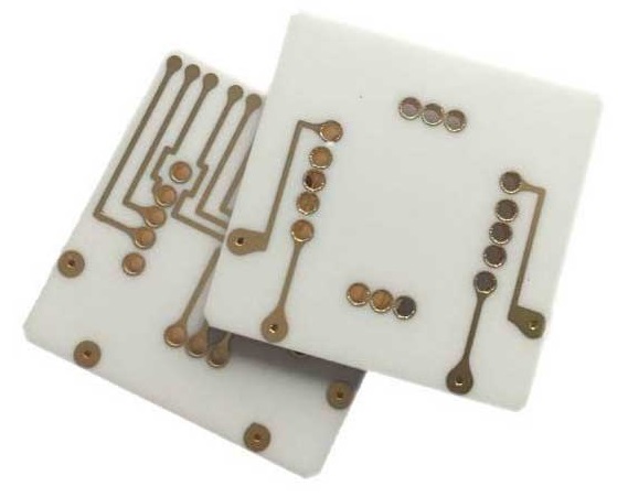
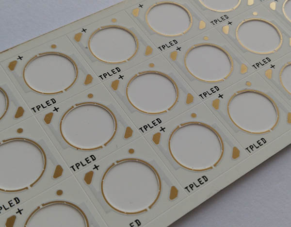
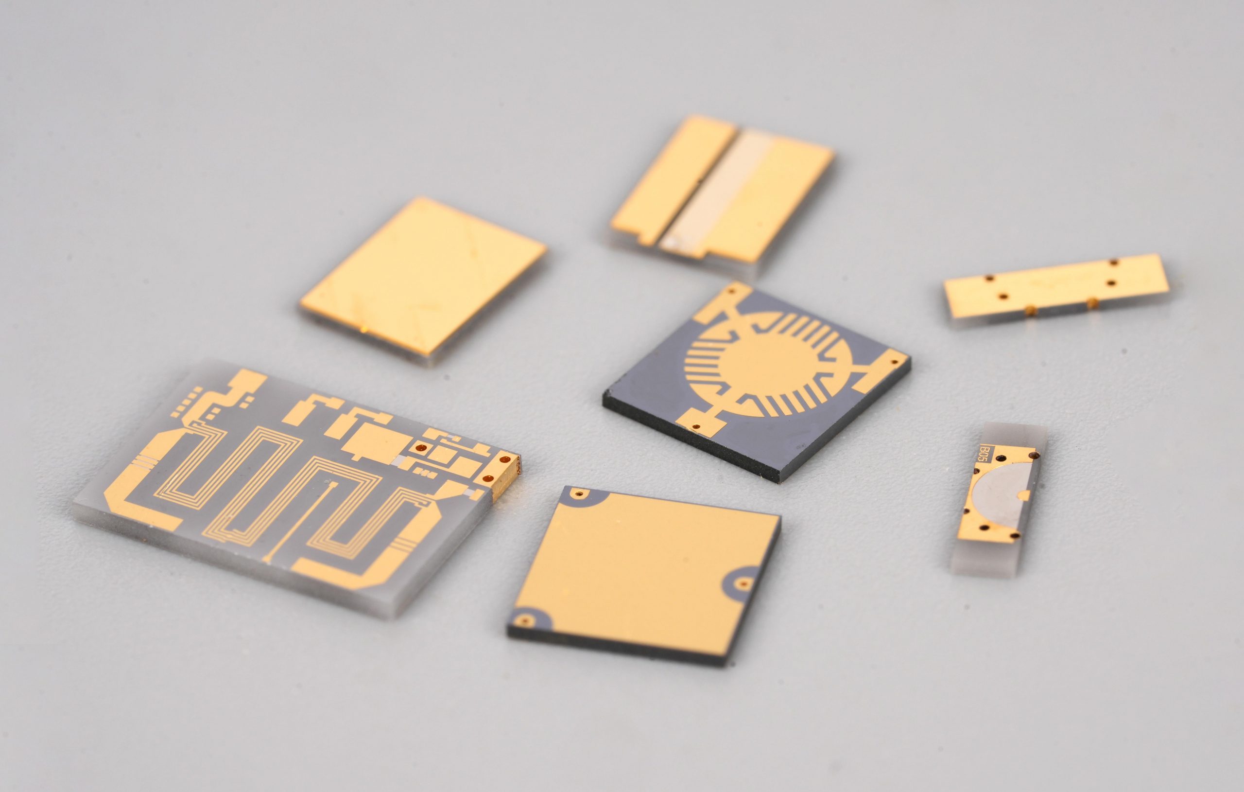
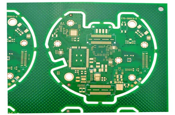
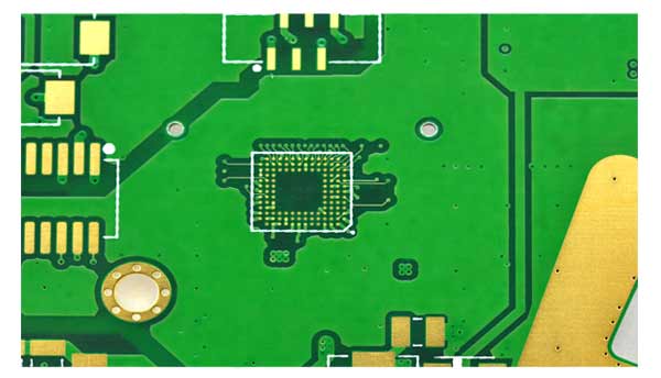
AlN laser cutting is commonly used in industries such as electronics, automotive, aerospace, and telecommunications. In the electronics industry, AlN is often used for components like heat sinks, substrates, and high-power devices that require both thermal conductivity and electrical insulation. In aerospace and automotive sectors, AlN is used for its ability to withstand high temperatures and provide efficient heat dissipation.
Given the growing demand for miniaturized and high-performance components, AlN laser cutting is becoming increasingly popular for fabricating small, complex parts that need to meet high reliability standards.
What Are Common Problems Occurred During AlN Laser Cutting?
While AlN laser cutting offers numerous advantages, it’s not without its challenges. One of the most common issues is blackening along the cut edges. Other problems include excessive heat buildup, poor edge quality, material cracking, and the formation of burrs. Each of these issues can affect the overall performance of the component and increase post-processing requirements.
However, most of these problems can be mitigated with proper adjustments to the laser cutting parameters and the right choice of assist gases. Understanding the root causes of these issues is essential for improving the quality and efficiency of the laser cutting process.
Why Does AlN Blacken During Laser Cutting?
Blackening during AlN laser cutting occurs primarily due to oxidation and overheating. Here’s a breakdown of the causes:
Oxidation: AlN is a combination of aluminum and nitrogen. When exposed to high heat from the laser, especially in the presence of oxygen, the aluminum reacts with the oxygen to form aluminum oxide (Al₂O₃). This oxide layer appears as a dark, blackened surface, which is often undesirable for aesthetic and functional reasons.
Overheating: If the laser power is too high or the cutting speed is too slow, excess heat can build up in the AlN material. This can lead to degradation, resulting in the formation of carbon or other residues that further contribute to blackening.
Assist Gases: The choice of assist gases plays a significant role in the oxidation process. Oxygen-based gases promote oxidation, while inert gases like nitrogen help prevent it. If the wrong gas is used or the pressure is incorrectly adjusted, the material can oxidize, leading to unwanted blackened edges.
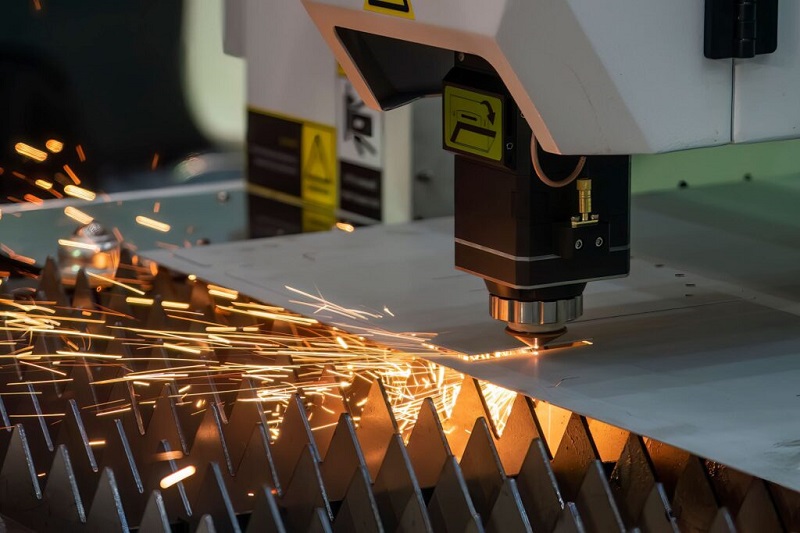
What Is the Role of Laser Power and Speed in AlN Cutting Quality?
Laser power and speed are two crucial factors that directly influence the quality of AlN cuts. Here’s how each affects the process:
Laser Power: High laser power can easily overheat the material, increasing the chances of oxidation and degradation. Reducing the laser power ensures that the material is not exposed to excessive heat, helping to maintain the integrity of the cut and preventing blackening. It also allows for more controlled cutting, especially for thin AlN materials.
Cutting Speed: The speed at which the laser moves across the material is equally important. If the laser moves too slowly, it can lead to excessive heat accumulation in one spot, leading to overheating and blackening. On the other hand, if the speed is too fast, the laser may not have enough time to make a clean cut. Finding the right balance between power and speed is key to achieving clean, high-quality cuts
How Assist Gases Affect AlN Laser Cutting and Blackening
Assist gases are used in laser cutting to clear the molten material from the cut area and help with heat dissipation. They also have a significant impact on the final surface quality of AlN cuts:
Nitrogen: Nitrogen is an inert gas that doesn’t react with the material. It creates a non-oxidizing atmosphere that helps prevent blackening and oxidation. Using nitrogen as an assist gas is ideal for cutting AlN without introducing unwanted discoloration.
Oxygen: Oxygen is often used when cutting materials that require faster cutting speeds. While it improves cutting efficiency, it also increases the likelihood of oxidation, leading to blackened edges. Careful control of oxygen pressure and flow can help minimize this effect.
Air: Air contains oxygen, which promotes oxidation. Using air as an assist gas for AlN laser cutting is generally not recommended, as it can exacerbate the blackening issue. If air is used, adjustments to other parameters (like laser power and speed) will be necessary to avoid oxidation.
How to Prevent Blackening During AlN Laser Cutting
Preventing blackening during AlN laser cutting involves several strategies:
Adjust Laser Power and Speed: Reduce the laser power to prevent overheating, and adjust the cutting speed to minimize heat buildup. Balancing these two factors is essential for clean cuts.
Use Nitrogen as an Assist Gas: Nitrogen prevents oxidation and helps maintain the material’s quality during cutting. Ensure that nitrogen pressure is high enough (between 5-10 bar) to help expel molten material from the cutting zone.
Proper Laser Focusing: Ensure the laser is properly focused to control the heat distribution. A well-focused laser beam reduces the chances of excessive heat and blackening.
What Is the Best Cooling Method for Preventing Overheating and Blackening in AlN?
Effective cooling is essential for preventing overheating, which can lead to blackening. Some of the best cooling methods include:
Air Cooling: Using compressed air or directed air streams can help dissipate excess heat from the cutting zone, preventing the material from overheating.
Water-Cooled Beds: Incorporating water-cooled beds or a water-based cooling system can also help regulate the temperature during cutting, ensuring that the AlN material remains at an optimal temperature.
Controlled Ambient Temperature: Maintaining a stable temperature in the cutting environment can also reduce the risk of overheating, especially in high-precision applications.
Are There Post-Processing Techniques to Restore AlN Surfaces After Laser Cutting?
If blackening does occur during AlN laser cutting, there are several post-processing methods that can help restore the material’s appearance:
Chemical Cleaning: Acid washing using hydrochloric or phosphoric acid can remove oxidation and restore the AlN surface without damaging the material.
Mechanical Polishing: For larger areas of blackening, mechanical polishing with abrasive pads can smooth out the surface and remove any discoloration.
Laser Polishing: A more advanced technique, laser polishing, involves using a laser to melt the surface slightly and smooth out imperfections. This method provides a highly precise finish and can be used to remove any blackened areas.
Blackening during AlN laser cutting is a common issue that can affect both the aesthetic and functional properties of the material. However, by optimizing laser parameters, choosing the right assist gases, and incorporating cooling systems, manufacturers can significantly reduce or eliminate blackening. Additionally, post-processing techniques like chemical cleaning and polishing can further improve the surface quality. With the right approach, you can achieve clean, high-quality AlN cuts that meet both performance and appearance standards.
Have you encountered blackening during AlN laser cutting? Just feel free to share your experiences and tips in the comments below. Whether you need multiple types of Ceramic PCB products or a customized solution, EBest Circuit (Best Technology) provides excellent service and fast delivery. You can reach us at sales@bestpcbs.com for more information or inquiries.