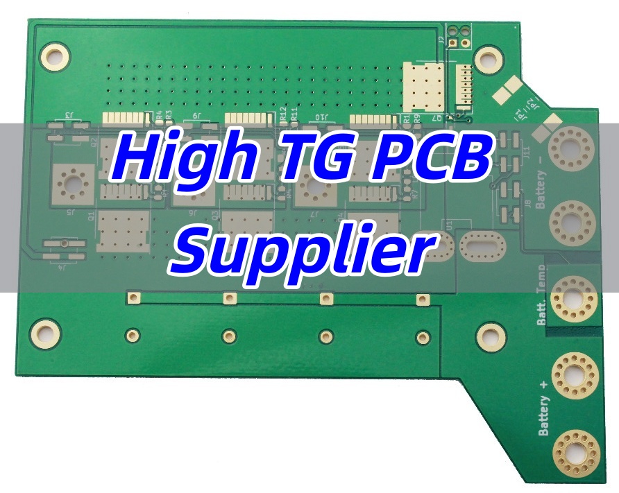
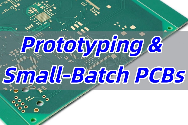
Why choose high-layer & custom PCB? Let’s discover definition, pros and cons, applications, design spec and guide, production process for high-layer & custom PCBs.
Are you troubled with these questions?
- High-layer PCB suffers from signal interference and unstable performance – how to resolve?
- Multiple customization demands lead to extended R&D cycles and high costs – what’s the solution?
- Stringent process requirements result in low production yield and delivery delays – how to improve?
As a high-layer and custom PCB manufacturer, EBest Circuit (Best Technology) can provide you service and solutions:
- Intelligent Layer Stackup Optimization – Reduce signal loss by 15% for 12+ layer PCBs, achieve over 92% first-pass success rate in trial production, ensuring stable performance.
- Rapid Prototyping Service – Complete complex custom orders in 72 hours with 40% shorter delivery cycles, enabling flexible R&D scheduling.
- Cost Optimization Strategy – Precisely match materials and processes to reduce overall costs by 18%-25%, maximizing budget efficiency and profit margins.
Welcome to contact us if you have any request for high-layer and custom PCBs: sales@bestpcbs.com.
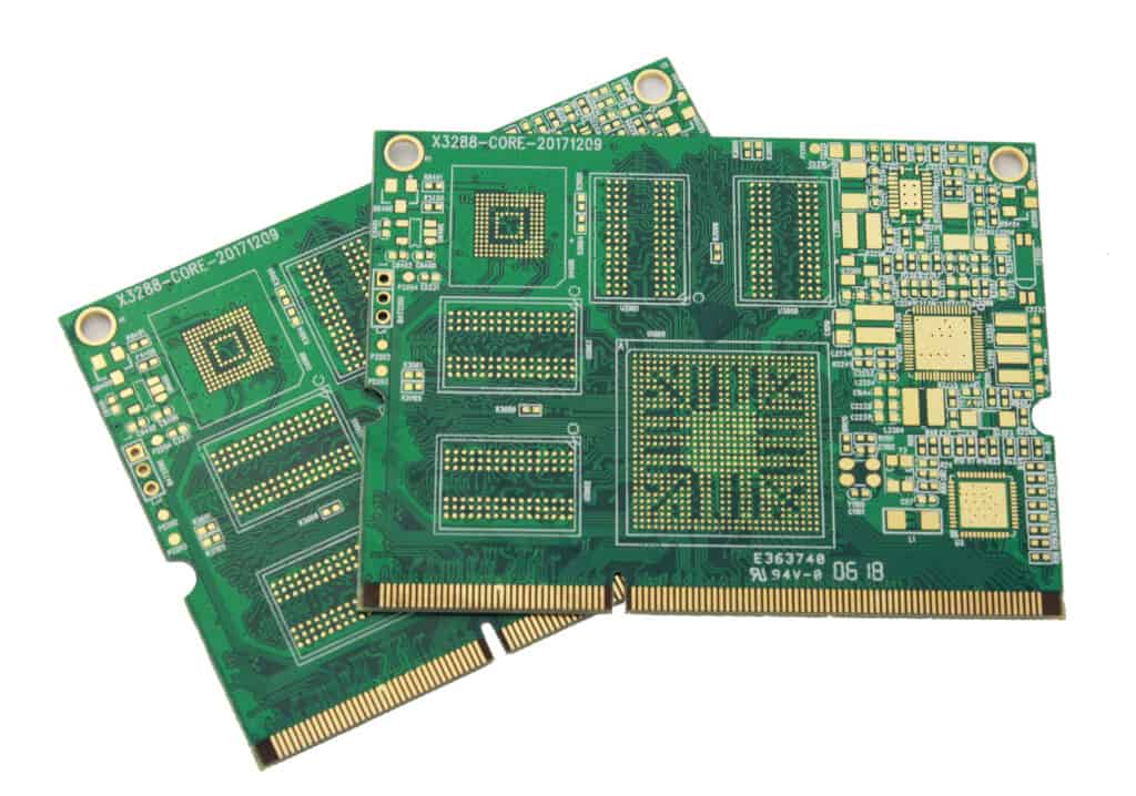
What Is High-Layer & Custom PCB?
High-layer and custom PCBs are two core PCB solutions for high-performance electronic system design. They integrate technologies to meet the needs of complex scenarios:
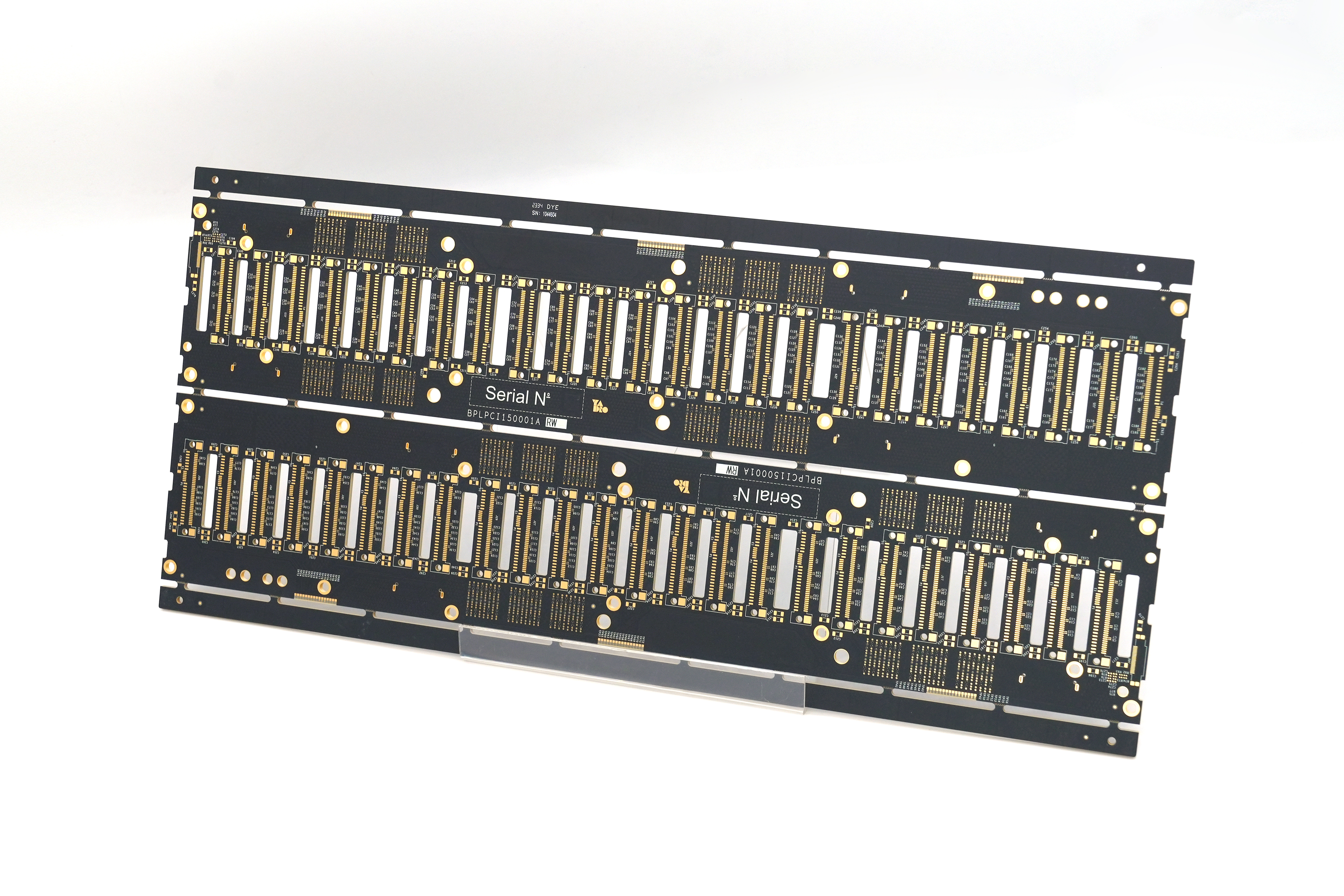
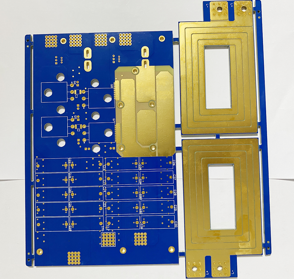
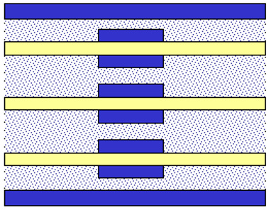
High-layer PCBs utilize multiple stacked conductive and insulating layers (typically 12 or more). Designed specifically for complex electronic devices, they support high-density wiring, high-speed signal transmission, and high-performance requirements.
Custom PCBs are customized to meet specific customer needs. They offer flexible adjustments to the number of layers (single or multi-layer), materials (such as aluminum or polyimide), size, shape, and special features (such as high-frequency signal processing and high-temperature resistance) to meet unique design requirements or optimize space utilization.
The two form a combined advantage of “high performance + strong adaptability” – the high-layer structure as the underlying architecture of customized design supports high-density interconnection requirements, and the customization capability gives the high-layer PCB a wider range of application adaptability, promoting the evolution of electronic systems towards high integration, high reliability and high energy efficiency.
What Are Pros and Cons of High-Layer & Custom PCB?
Advantages
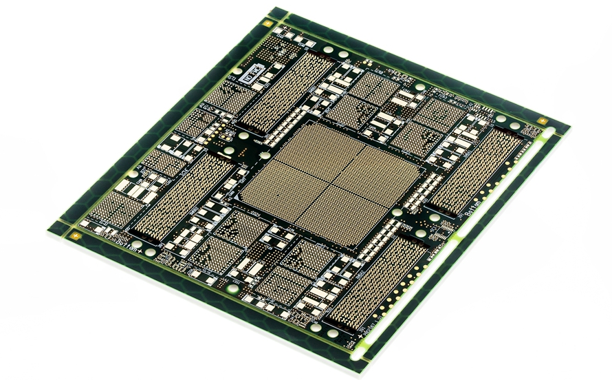
- Performance Enhancement and Functional Integration: Enables integration of high-speed digital, analog, RF, and high-power circuits on a single board, providing physical foundation for “All-in-One” premium devices like high-end servers and medical imaging systems.
- Signal and Power Integrity Assurance: Dedicated signal layers with complete ground/power planes minimize signal distortion, delay, and crosstalk, while multi-layer power systems ensure stable, low-noise power delivery for high-power chips like multi-core processors, enhancing system stability.
- Miniaturization and Structural Optimization: High routing density allows compact designs within the same footprint, supporting advanced technologies like HDI and rigid-flex combinations to meet special form factors such as foldable and wearable devices.
- Exceptional Reliability and Quality: Multi-layer stacked structures enhance mechanical strength and thermal stability, performing better under vibration, shock, and temperature cycling. Specialty materials and strict process controls meet extreme reliability and lifespan demands in aerospace, automotive, and medical sectors.
- Long-Term Technological Barrier: Highly customized designs (materials and structure) are hard to replicate, helping clients build unique competitive advantages and form technical moats.
Disadvantages
- High Economic Costs: Unit prices significantly exceed standard PCBs due to premium materials, complex processes (e.g., laser drilling, multi-lamination), and extended lead times. Development involves substantial NRE costs for custom tooling, simulation, and prototyping.
- Extended Timelines: Design requires extensive simulation and iteration, demanding skilled engineers and advanced EDA tools. Manufacturing spans weeks to months, limiting agility in fast-paced markets.
- Elevated Technical and Collaboration Barriers: Reliance on a small pool of high-end manufacturers restricts supply chain flexibility. Success hinges on close collaboration between client and manufacturer from early design stages, where miscommunication or DFM oversights risk delays or failures. Design changes post-finalization incur steep costs, often requiring rework.
- Yield and Quality Risks: Increased complexity with more layers raises risks of lamination misalignment, inner-layer defects, and drilling issues, potentially impacting final yield and long-term reliability.
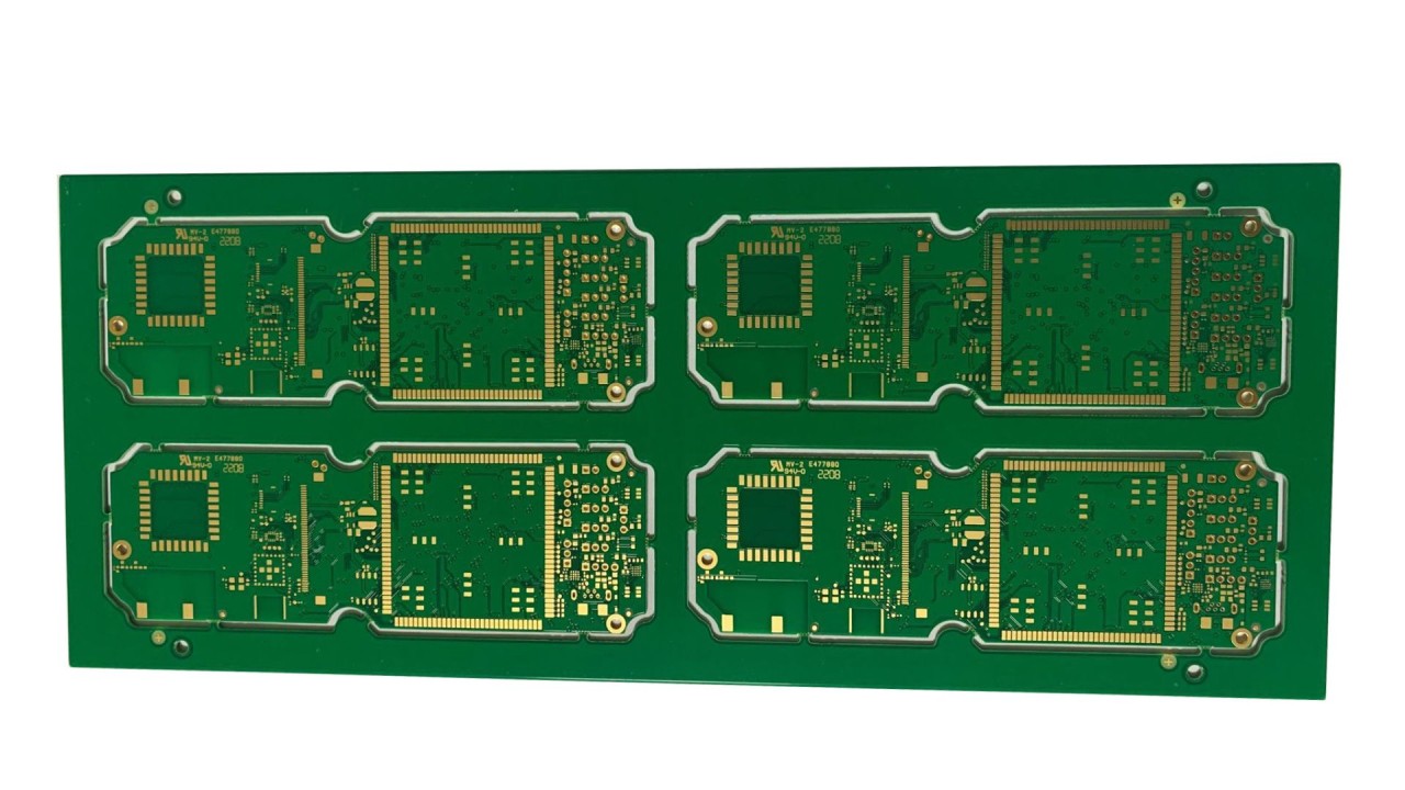
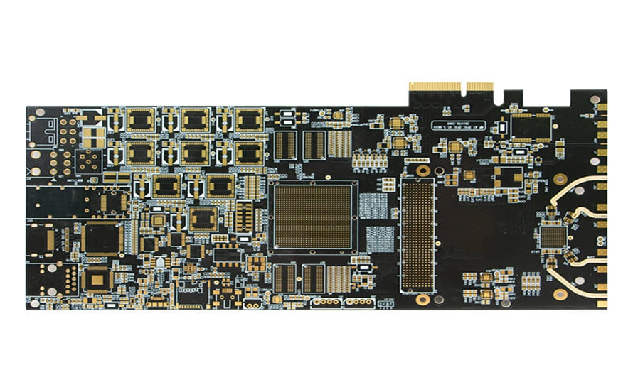
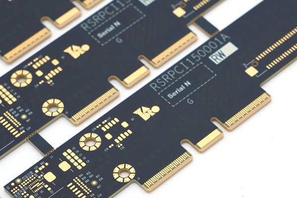
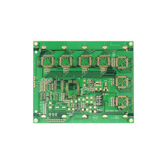
What Are Applications of High-Layer & Custom PCBs?
- AI training server: GPU cluster interconnect motherboard
- High-speed switch: 100G/400G Ethernet backplane
- Storage array controller: PCIe 5.0 RAID controller card
- 5G base station: Massive MIMO antenna array control board
- Optical module: 800G Coherent DSP driver board
- Satellite communication: Ka-band phased array TR module
- Airborne radar: Active electronically scanned array (AESA) power control board
- Missile guidance: Inertial navigation system core board
- Satellite payload: Intersatellite laser communication transceiver board
- CT scanner: X-ray tube high-voltage generator module
- MRI equipment: Gradient coil power amplifier
- Surgical robot: Multi-axis motion control motherboard
- Autonomous driving domain controller: Multi-sensor fusion processing board
- In-vehicle Ethernet gateway: DoIP protocol switch board
- Battery management system: EV high-voltage sampling board
- Semiconductor tester: Probe card interface board
- High-speed oscilloscope: ADC sampling front-end board
- Industrial PLC: Multi-axis servo drive control board
High-Layer & Custom PCB Design Specification
| Category | Technical Parameters |
| Layer Stackup Design | Layer count ≥8, adopting alternating ‘Signal-Ground-Power-Signal’ structure (e.g., 10-layer board: S1-GND-S2-PWR-S3-S4-GND-S5-PWR-S6) |
| Impedance Control | Differential line length error ≤5mil; dynamic adjustment of trace width/dielectric thickness (e.g., 100Ω differential pair: trace width 4.5mil/spacing 4mil) |
| Routing Rules | 3W Rule: Parallel signal line center spacing ≥3× trace width (e.g., 5mil trace width, spacing ≥15mil) |
| High Voltage Isolation | Line spacing ≥1.5mm in 250VAC environment; slot isolation between HV/LV zones (slot width ≥1mm, through-board) |
| Zoning Layout | Digital/analog circuit spacing ≥2mm; I/O port isolation >2mm |
| EMC Design | Power/ground planes must be adjacent; decoupling capacitor distance to IC pin ≤200mil; power trace width ≥40mil |
| High Frequency Shielding | RF zone uses embedded shielding materials (e.g., ECCOSORB, 97dB/cm attenuation at 40GHz) |
| Safety Clearance | Primary/secondary circuit clearance ≥6.4mm (240V AC), +20% in humid environments |
| Thermal Via Array | Thermal vias under power devices (via diameter ≥8mil, spacing ≤1.5mm, connected to inner ground plane) |
| Copper Thickness | High-current paths ≥2oz; grid copper pour to reduce thermal warpage |
| Pad Design | Pad diameter ≥16mil larger than drill hole; non-plated holes marked ‘NPTH’ |
| Panelization Rules | Panels required for dimensions <50mm×50mm; R5 fillet on process edge; V-cut depth 1/3 board thickness |
| Silkscreen Marking | Silkscreen width ≥5mil, height ≥50mil; no coverage on pads/fiducials |
| High Frequency Substrate | Ultra-low loss materials: LCP substrate (εr=2.9@40GHz) or carbon nanotube resin |
| Board Thickness Tolerance | Standard board thickness ±10% (e.g., 1.6mm±0.16mm) |
| DFM Inspection | Component spacing ≥1mm; board edge clearance >2mm; aspect ratio recommended 3:2 or 4:3 |
| Simulation Requirements | Mandatory SI/PI simulation for high-speed boards (using Ansys/Cadence toolchain) |
How to Design a High-Layer & Custom Printed Circuit Board?
High-Layer & Custom Printed Circuit Board Design Guide:
1. Requirement Analysis and Specification Definition
- Electrical Performance Boundaries: Define hard indicators such as signal rate (e.g., 5Gbps), impedance tolerance (±10%), and power noise threshold (<50mVpp) for high-frequency digital circuits.
- Mechanical Constraint Quantification: Derive PCB maximum outline from product enclosure dimensions, reserve assembly clearance (±0.2mm) to prevent later assembly interference.
- Thermal Design Pre-planning: Calculate heat dissipation requirements via power device thermal resistance (RθJA), e.g., for a processor with TDP=10W, plan copper foil area ≥2000mm² or add thermal via arrays.
2. Stack-Up Structure Design
- Classic Stack-Up Template: For 8-layer boards, recommend “Signal-Ground-Power-Signal-Signal-Power-Ground-Signal” structure to ensure high-speed signals are surrounded by reference planes.
- Interlayer Dielectric Control: Use materials with stable dielectric constant (e.g., FR4-TG150), control interlayer dielectric thickness error within ±10% to avoid impedance fluctuation.
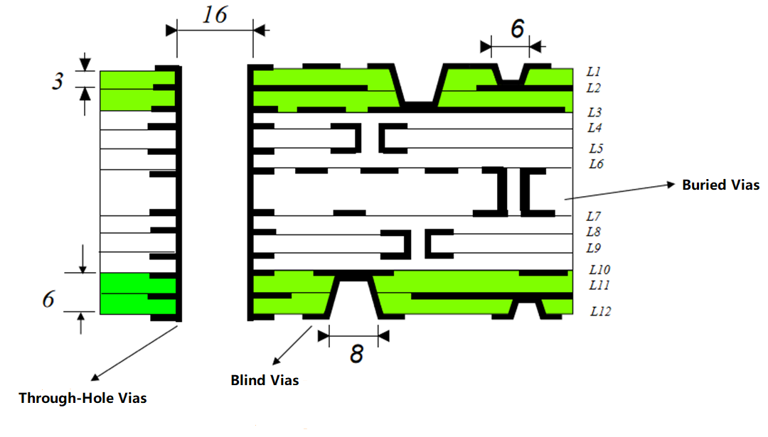
- Blind/Buried Via Optimization: In BGA package areas, adopt 1+N+1 blind via structures (e.g., L1-L2 blind via + L2-L7 through via + L7-L8 blind via) to reduce interlayer signal path length.
3. Signal Integrity Design
- Impedance Control: Calculate microstrip/stripline impedance using Polar SI9000 tools, e.g., 50Ω single-ended trace requires trace width=6mil (FR4, Dk=4.2, thickness=1.2mil).
- Crosstalk Suppression: Maintain 3W principle (W=trace width) for differential pair spacing, parallel signal trace spacing ≥2× trace width, and use “ground enclosure” routing for critical signals.
- Length Matching: Achieve ±50mil length tolerance for DDR4 data lines via serpentine routing, use Allegro “Accordion” function for automatic trace length adjustment.
4. Power and Ground Plane Design
- Power Zoning: Isolate digital/analog/RF power domains via beads/inductors, e.g., connect digital 3.3V and analog 3.3V_A with 10Ω beads.
- Decoupling Capacitor Placement: Follow “large capacitor (100μF) remote + small capacitor (0.1μF) proximity” principle to form low-to-high frequency filtering network.
- Ground Plane Segmentation: Avoid ground plane cuts under high-speed signals; if necessary (e.g., audio zone), use single-point ground bridging to prevent ground bounce noise.
5. Thermal Management Design
- Heat Dissipation Path: Deploy thermal via arrays (spacing 1mm, diameter 0.3mm) under power components to transfer heat from top layer to bottom heatsink.
- Material Thermal Conductivity Upgrade: Use Rogers RO4350B (thermal conductivity 0.6W/mK) for high-frequency scenarios, combine with copper substrate (thermal conductivity 400W/mK) for localized high-heat zones.
- Thermal Simulation Validation: Perform thermal flow simulation with Ansys Icepak to ensure maximum temperature rise ≤30°C (ambient 25°C), preventing PCB deformation from thermal stress.
6. Material and Process Selection
- Substrate Selection Logic: FR4 for low-frequency (<1GHz), RO4350B for high-frequency (>1GHz), Taconic TLX-8 for RF (>10GHz).
- Surface Finish Comparison: ENIG for high-frequency connectors, HASL for general digital circuits, avoid OSP failure in multi-layer boards due to high temperatures.
- DFM Verification: Use Altium Designer “DRC” function to check trace width/spacing (≥4mil), via size (≥8mil), and routing density (≤80% routing channel).
7. Simulation and Validation Closed Loop
- Signal Integrity Simulation: Perform eye diagram analysis via HyperLynx to ensure eye height >300mV, eye width >80%UI, meeting protocols like PCIe 3.0.
- Power Integrity Verification: Analyze power plane impedance with SIwave to ensure impedance <10mΩ at target frequency (e.g., 100MHz), preventing voltage drop.
- Prototype Validation: After engineering prototype fabrication, measure S-parameters with network analyzer, capture eye diagrams with oscilloscope, scan hotspots with thermal imager, forming “simulation-measurement-correction” closed loop.
How to Make a High-Layer & Custom Printed Circuit Board?
High-Layer & Custom Printed Circuit Board Production Process
1. Material Cutting and Substrate Preparation
- Substrate Selection: Choose low-loss high-frequency materials (e.g., RO4350B) or conventional FR4 substrates based on design requirements. Verify panel thickness (0.8mm-3.0mm), copper foil thickness (1/2oz-2oz), and layer count (8-32 layers).
- Panel Cutting: Use CNC cutting machines to trim large substrate rolls into standard sizes (e.g., 450mm×600mm), reserving 3-5mm processing allowance to avoid edge burrs affecting subsequent processes.
- Surface Cleaning: Remove oxidation layers and contaminants from the substrate surface via chemical cleaning or plasma treatment to enhance dry film adhesion.
2. Inner Layer Circuit Fabrication
- Dry Film Lamination: Apply photosensitive dry film onto cleaned substrates, ensuring no bubbles or wrinkles via hot rollers. Dry film thickness is controlled at 35-50μm.
- Exposure and Development: Use LDI (Laser Direct Imaging) equipment to transfer Gerber patterns onto the substrate. UV exposure energy is maintained at 80-120mJ/cm², with developer concentration at 1.0-1.2% and development time of 40-60 seconds.
- Etching and Stripping: Etch unprotected copper layers using acidic etchant (CuCl₂+HCl) at 1.5-2.0μm/min etching rate. After etching, rinse with high-pressure water to remove residual etchant and dry film.
3. Lamination and Stacking
- Stack-Up Construction: Arrange inner layers, prepregs, and copper foils in the designed sequence (e.g., alternating “signal-ground-power-signal” layers) using alignment pins to ensure interlayer alignment accuracy ≤±15μm.
- Vacuum Lamination: Press the stack in a vacuum press at 180-200℃ and 350-400psi for 2-3 hours, ensuring prepregs fully melt and fill interlayer gaps to form dense insulating layers.
- X-ray Drilling Positioning: Use X-ray drilling machines to locate inner-layer target holes, ensuring subsequent drilling accuracy ≤±50μm.
3. Drilling and Plating
- Mechanical Drilling: Drill via holes, blind holes, and buried holes using high-precision drills (15,000-20,000rpm) with diameters of 0.15-0.3mm and depth tolerance ≤±0.1mm.
- Laser Drilling: For blind/buried holes, use CO₂ or UV laser drilling with hole diameters as small as 50μm. Control laser energy to avoid carbon residues.
- Hole Metallization: Apply electroless copper plating (≥0.5μm) followed by electrolytic copper plating (≥25μm) to form conductive layers, ensuring no voids or seepage in hole walls.
4. Outer Layer Circuit and Impedance Control
- Outer Layer Dry Film and Exposure: Repeat inner-layer processes for outer-layer circuits, with strict control of line width/spacing tolerances (≤±10%) for impedance-matched traces (e.g., 50Ω single-ended, 100Ω differential).
- Impedance Testing: Use TDR (Time Domain Reflectometry) testers for in-line inspection of critical signal lines to ensure impedance values meet design requirements (e.g., ±10% tolerance).
5. Surface Finish and Solder Mask
- Surface Treatment: Select ENIG (Electroless Nickel Immersion Gold), HASL (Hot Air Solder Leveling), or OSP (Organic Solderability Preservative) based on design needs to ensure solderability and corrosion resistance.
- Solder Mask Printing: Apply solder mask ink via screen printing or spraying at 20-30μm thickness. After pre-baking, exposure, and development, form precise solder mask patterns.
6. Profiling and Testing
- CNC Profiling: Cut PCB outlines using CNC routing machines with accuracy ≤±0.15mm, ensuring burr-free and delamination-free edges.
- Electrical Testing: Use flying probe testers or fixture testing for open/short circuit and impedance verification, ensuring 100% coverage of critical nets.
- AOI Inspection: Deploy automated optical inspection (AOI) systems to detect line, solder mask, and surface finish defects with false rejection rate ≤100ppm.
7. Packaging and Shipping
- Cleaning and Drying: Remove surface static using ionized air blowers. Prior to vacuum packaging, perform high-temperature drying (60℃/2 hours) to eliminate moisture.
- Vacuum Packaging: Use double-layer packaging (anti-static bag + aluminum foil bag) with humidity indicator cards to maintain storage humidity ≤30%RH.
- Labeling and Traceability: Attach labels containing batch numbers, production dates, and customer information. Generate traceable manufacturing archives (including process parameters and test data).
Why Choose EBest Circuit (Best Technology) as High-Layer & Custom PCB Manufacturer?
Reasons why choose us as high-layer & custom PCB manufacturer:
- 19 Years of Manufacturing Expertise: Decades of experience serving over 5000 enterprises across high-layer PCBs, HDI boards, and rigid-flex combinations, reducing R&D trial costs by 20% through proven process knowledge.
- Global Certification Compliance: Certifications include ISO 9001, IATF 16949 automotive quality standards, medical-grade ISO 13485, and RoHS environmental compliance, meeting EU, North American, and other regional market requirements.
- Competitive Pricing Advantage: Through scaled production and optimized supply chain management, customers achieve 15%-20% average cost reduction compared to industry benchmarks, particularly for cost-sensitive applications in consumer electronics and industrial control.
- Cost-Sensitive Design Solutions: Free DFM (Design for Manufacturability) analysis leverages 19 years of expertise to optimize circuit layouts, material selection, and process parameters, reducing design iteration costs by over 30% and accelerating time-to-market.
- 24-Hour Rapid Prototyping for Urgent Orders & Low MOQ: Support 5 piece MOQ and 24 Hours rapid prototyping for urgent orders to reduce time to market.
- Emergency orders activate priority channels, delivering samples within 24 hours from design file receipt, critical for time-sensitive industries like medical devices and automotive electronics.
- 99.2% On-Time Delivery Rate: Intelligent production scheduling and dynamic inventory systems achieve 99.2% on-time delivery, surpassing the industry average of 95% to ensure stable production planning.
- Comprehensive Quality Control: 100% batch inspection with 8-step processes including AOI optical inspection, flying probe testing, and X-ray analysis maintains defect rates below 0.03%, 40% lower than industry standards.
- Advanced Customization Capabilities: Support for complex architectures from 2-layer to 64-layer HDI, high-frequency/high-speed boards, and embedded component boards with 3mil minimum line/space widths for 5G and AI applications.
- End-to-End Technical Support: Dedicated engineering teams provide 24/7 support covering design consultation, prototype validation, and mass production, ensuring 98%+ issue resolution rates and enhanced product reliability.
How to Get a Quote for Your High-Layer & Custom PCB Project?
To obtain a quote for your high-layer and custom PCB project, submit the following 10 quotation checklist items to ensure precise and efficient pricing:
- Complete Design File Package: Gerber format layer-by-layer circuit data, drilling files (.drl/.txt), coordinate files (CSV), and PCB engineering drawings with annotations for board thickness, hole diameter, and layer stack-up structure.
- Bill of Materials (BOM): Component names, models, quantities, supplier information, and non-standard component dimensions (e.g., IC package types, resistor sizes).
- Process Parameter Details: PCB layer count (4-64 layers), board thickness (0.8-3.2mm), copper thickness (0.5-3oz), surface finishes (ENIG/HASL/OSP), solder mask color, and minimum trace width/spacing (e.g., 3mil).
- Special Process Specifications: Blind/buried via requirements, high-frequency material specifications (e.g., Rogers 4350B), embedded capacitor/resistor zones, and rigid-flex area markings.
- Environmental & Certification Requirements: RoHS compliance declaration, ISO 13485 (medical grade), IATF 16949 (automotive grade) certificate numbers, and corresponding product zones.
- Testing Standard Documents: Electrical performance tests (e.g., impedance matching), functional tests (FCT), aging test protocols, and AOI/X-ray inspection requirements.
- Order Quantity & Lead Time: Initial order volume (e.g., 500 pieces/10,000 pieces), annual demand forecast, urgent order flags (24-hour prototyping), and standard lead times (15-20 days).
- Packaging & Logistics Requirements: Vacuum packaging standards, moisture barrier bag specifications, shipping methods (air/sea freight), and destination port/airport codes.
- DFM Analysis Request: Free Design for Manufacturability analysis request (including design optimization suggestions), process feasibility assessments (e.g., 0.1mm minimum hole diameter viability).
- Customer-Specific Requirements: Process edge dimensions, fiducial mark positions, panelization methods (V-cut/stamp holes), and eco-friendly packaging material requests.
Welcome to contact us if you have any inquiry for high-layer and custom PCBs: sales@bestpcbs.com.