The electronics industry has continuously pursued smaller and faster electronic products with increased functionality. To meet these demands, the electronic packaging industry has focused on developing more advanced packaging methods, aiming to increase the density of components on a circuit board while integrating multiple functions into a densely package.
The increasing density of packaging and interconnection has driven the progression of assembly methods from through-hole technology (THT) to surface-mount technology (SMT). Additionally, the use of wire bonding to connect chips to substrates has become more prevalent. The adoption of smaller interconnect pitches and chip-scale packaging (CSP) has further increased component density, while multi-chip modules (MCM) and system-in-package (SiP) have enabled the integration of more functions on a single package.
This post describes the key factors affecting the reliability of interconnections, with a particular focus on the specific properties of surface-treated wire bonding, emphasizing the selection of wire bonding surface treatments.

Selection of Surface Treatment for Wire Bonding
While electroless nickel gold provides excellent performance for wire bonding, it has three main drawbacks that hinder its application in cutting-edge technologies:
1. The relatively high demand for gold layer thickness leads to lengthy process costs.
2. Thick gold layers are prone to the formation of weak tin-gold intermetallic compounds (IMC), reducing the reliability of solder joints. To enhance solder joint reliability, alternative surface treatments may be used, but this increases additional process costs.
3. The electroplating process requires the use of electroplating lines, limiting the design freedom and wiring density of the packaging substrate.
The limitations posed by electroplated nickel-gold provide an opportunity for the adoption of chemical plating. The techniques of chemical plating include Electroless Nickel Immersion Gold (ENIG), Electroless Nickel Electroless Gold (ENEG), and Electroless Nickel Palladium Immersion Gold (ENEPIG).
Among these three options, ENIG is generally unproblematic due to its lack of high reliability in gold wire bonding properties (although it has been used in some low-end consumer products). On the other hand, ENEG shares the high production cost and presents complex challenges in terms of the manufacturing process, similar to electroplated nickel-gold.
ENEPIG was initially introduced in the late 1990s, its market acceptance was delayed until around the year 2000 due to fluctuations in palladium metal prices (which were inflated to unreasonable levels around 2000). However, ENEPIG can meet the requirements of many new packaging applications, providing reliable performance and conform to lead-free/ROHS requirements, with a recent strong surge in market demand.
In addition to the advantages in packaging reliability, the cost of ENEPIG is another benefit. With the recent rise in gold prices surpassing US$800/oz, it becomes challenging to control costs for electronic products requiring thick gold plating. The price of palladium (US$300/oz), relative to gold, is less than half, making palladium a cost-effective alternative with surface-related advantages.
Comparison of Surface Treatments
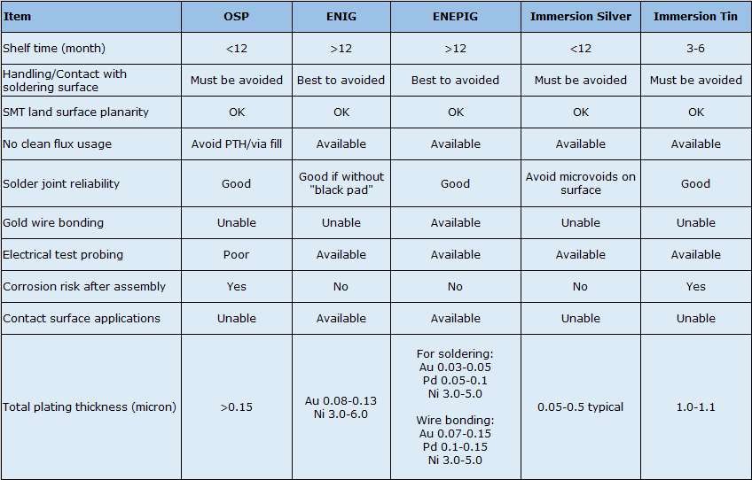
Up to now, for printed circuit boards accommodating fine-pitch QFP/BGA components, there are primarily four lead-free surface treatments:
Immersion Tin (IT)
Immersion Silver (IAg)
Organic Solderability Preservatives (OSP)
Electroless Nickel Immersion Gold (ENIG)
The table below compares these four surface treatments with ENEPIG. Among these surface treatments, none can simultaneously meet all the requirements of lead-free assembly processes, especially when considering multiple reflow experiences, pre-assembly shelf life, and gold wire bonding experiences. In contrast, ENEPIG offers good shelf life, solder joint reliability, gold wire bonding capability, and can serve as a touch button surface, providing surface-related advantages. Moreover, in the final gold replacement deposition reaction, the chemical palladium layer in ENEPIG works to protect the nickel layer, avoiding excessive corrosion during gold replacement.
What Are Advantages of ENEPIG?
ENEPIG has several crucial advantages, demonstrating reliable solderability and gold wire bonding concurrently. The key benefits are outlined as follows:
- Prevention of “Black Nickel Problem” – The absence of gold replacement attacking nickel on the surface prevents interfacial corrosion.
- The chemical palladium layer acts as a barrier, preventing copper from diffusing to the surface, ensuring satisfactory solderability.
- Palladium layer enable to completely dissolves in the solder, preventing the exposure of a high-phosphorus layer at the alloy interface. After the dissolution of the chemical palladium layer, the chemical nickel layer is revealed, forming a satisfactory nickel-tin alloy.
- Capability to Withstand Multiple Lead-Free Reflow Cycles
- Excellent Gold Wire Bonding Properties
These advantages make ENEPIG a preferred choice in various applications, ensuring reliable performance in both soldering and wire bonding processes while offering cost efficiency. As a one-stop PCB supplier in Asia, EBest Circuit (Best Technology) possesses advanced technology and high-tech manufacturing equipment that can meet the “multi-variety, small volume, high quality, strong capability, short delivery” requirements. Welcome to contact us if you are going to find a reliable circuit board manufacturer.