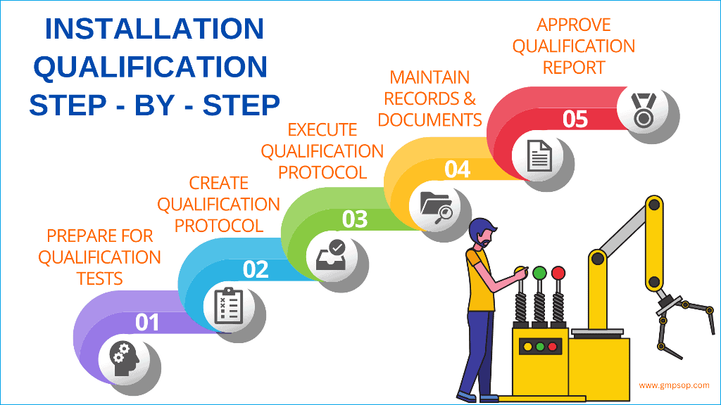
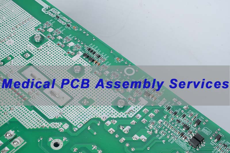
What Is Operational Qualification (OQ) in Medical PCBA Assembly?
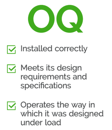
Operational Qualification (OQ) is the documented evidence that each step of the medical PCBA assembly process operates reliably within predefined and approved operating limits.
After Installation Qualification (IQ) confirms that equipment and systems are correctly installed, OQ focuses on a more critical question: does the process actually work as intended under controlled variation?
In medical electronics manufacturing, OQ represents the technical core of process validation. It is where engineering intent, manufacturing capability, and regulatory expectations converge.
Why Is OQ a Critical Requirement for Medical PCBA Manufacturing?
Medical devices rely on electronics that must perform consistently over long service lives, often in safety-critical or continuously operating environments. Final inspection alone cannot guarantee this level of reliability.
OQ is critical because it:
- Demonstrates that assembly processes are capable, stable, and repeatable
- Defines acceptable process windows rather than relying on nominal settings
- Reduces dependence on operator judgment
- Provides objective evidence for regulatory audits and OEM reviews
From a regulatory perspective, OQ shows that process risks are understood and controlled, not discovered after failures occur.
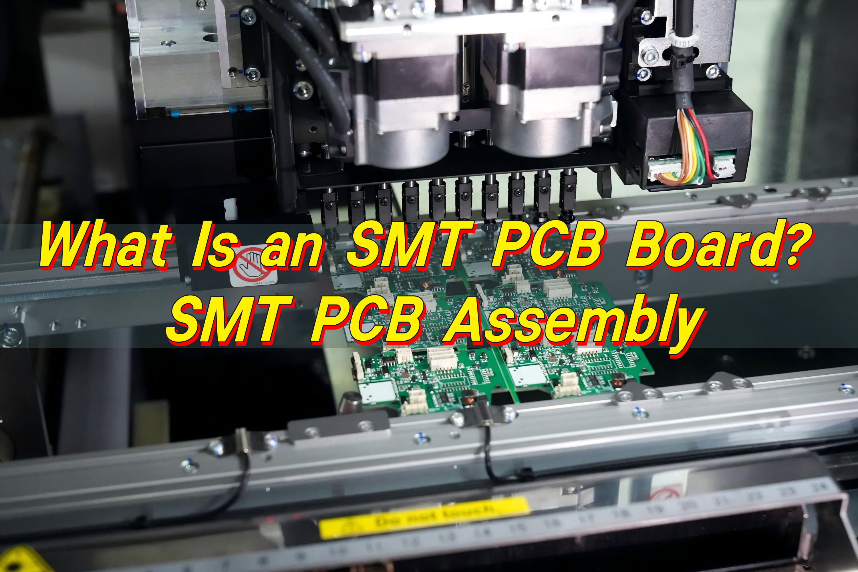
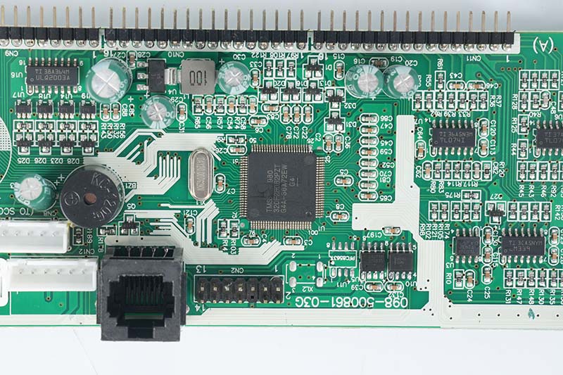
Which Assembly Processes Are Typically Validated During OQ?
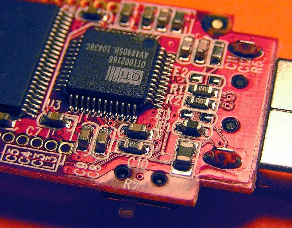
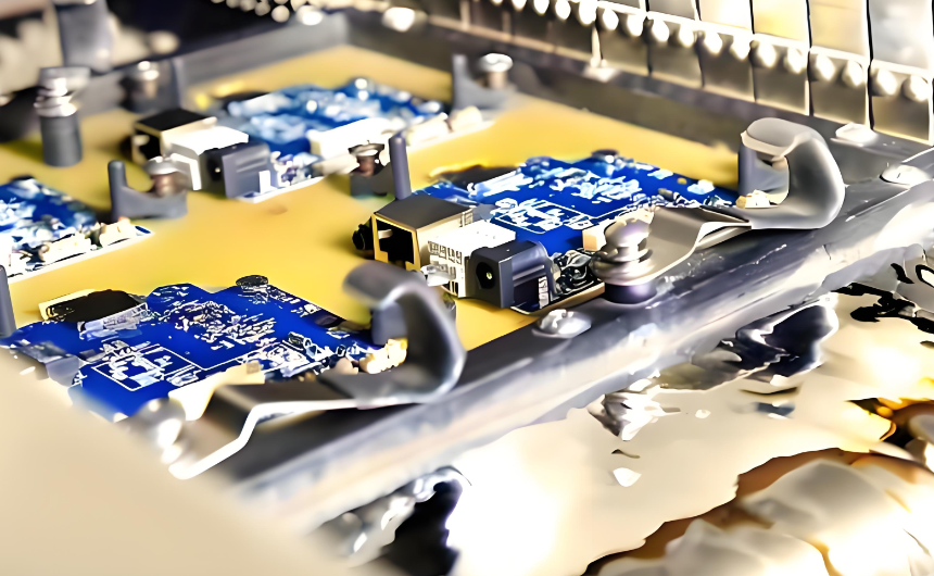
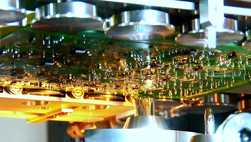
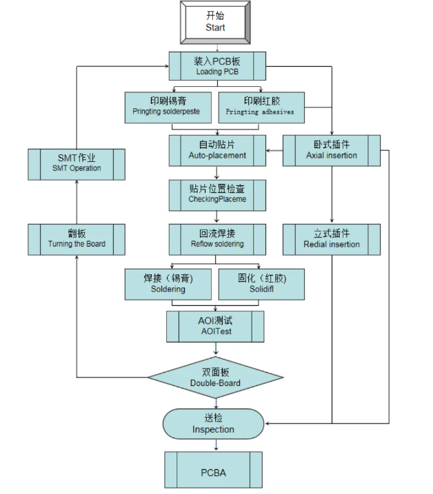
In medical PCBA assembly, OQ usually covers all process steps that can influence product quality, reliability, or compliance. At (EBest Circuit) Best Technology, typical OQ scope includes:
- Solder paste printing: print speed, squeegee pressure, stencil alignment, and paste release consistency
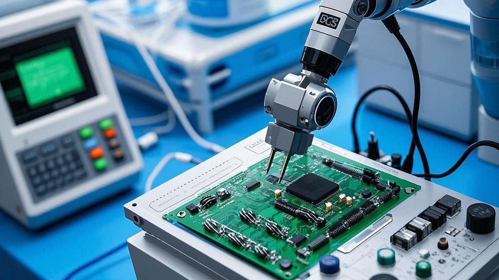
- Component placement: accuracy across different package sizes, fine-pitch components, and placement repeatability
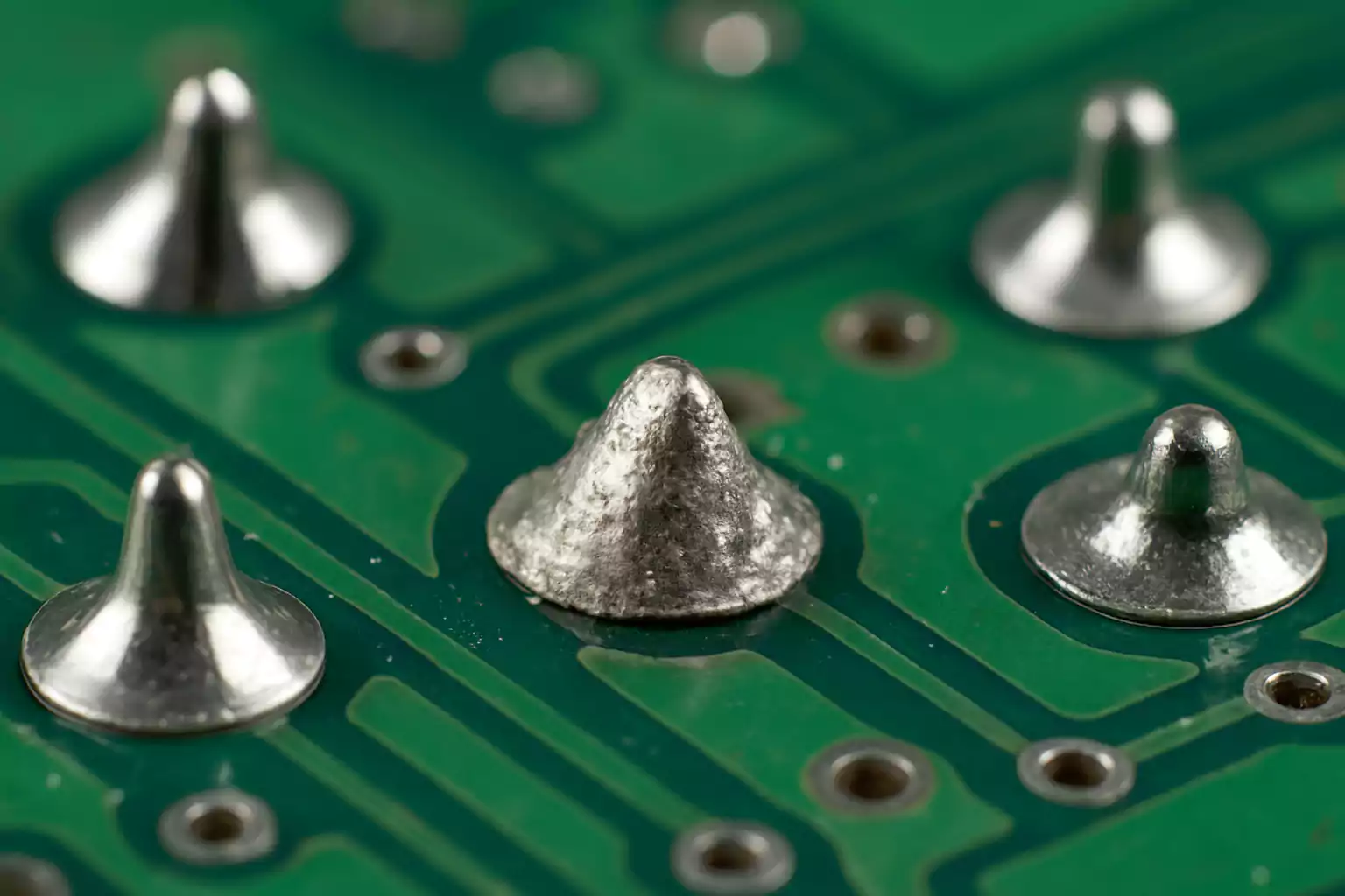
- Reflow soldering: temperature profiles validated at minimum and maximum limits, including soak, peak, and cooling zones
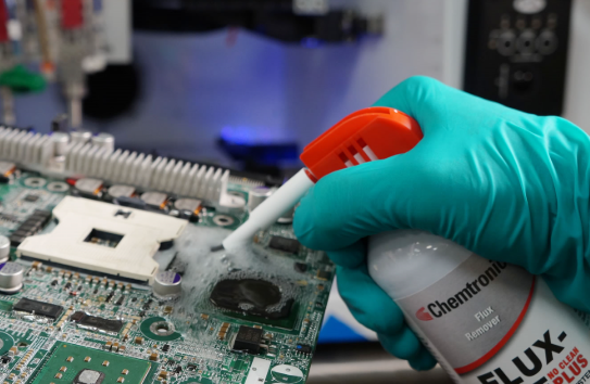
- Cleaning processes: effectiveness in meeting ionic contamination requirements
- Conformal coating (if applicable): thickness consistency, coverage, and curing parameters
- Functional and in-circuit testing: stability of results across defined operating ranges
Each process is evaluated not only at nominal conditions but also near its upper and lower operating limits.
How Does OQ Define Safe Process Windows?
One of the primary goals of OQ is to establish validated process windows. Instead of asking whether a process works once, OQ asks whether it continues to work when conditions vary within controlled boundaries.
For example:
- Can solder joints remain reliable if reflow peak temperature shifts slightly?
- Does placement accuracy remain acceptable across different component densities?
- Does cleaning effectiveness remain consistent at different throughput levels?
By answering these questions, OQ transforms unknown variability into documented, acceptable ranges, which is essential for medical PCBA reliability.
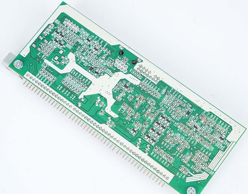
Why Is OQ Especially Important for Medical Electronics?
Medical PCBAs often involve:
- Fine-pitch and micro-pitch components
- High-density interconnects
- Mixed SMT and through-hole assembly
- Sensitive analog, sensing, or signal-conditioning circuits
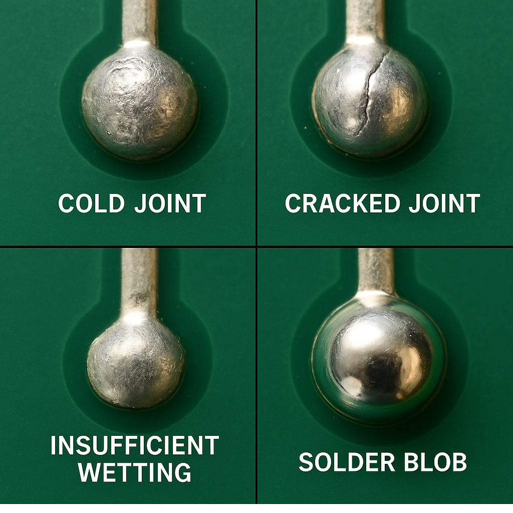
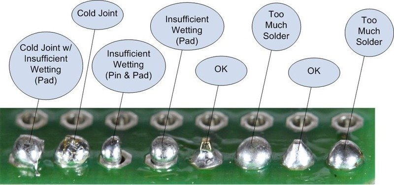
These characteristics make medical electronics highly sensitive to process variation. Minor deviations can create latent defects such as marginal solder joints or intermittent connections that pass inspection but fail during use.
OQ reduces this risk by ensuring that assembly processes remain stable even when operating near their defined limits.
How Does OQ Reduce Manufacturing and Patient Risk?
By validating process behavior under controlled variation, OQ helps prevent:
- Weak or inconsistent solder joints
- Thermal overstress or insufficient soldering
- Operator-dependent outcomes
- Process drift over time
In medical applications, such issues are not merely quality concerns—they can directly impact device safety, regulatory compliance, and patient outcomes. OQ provides the engineering evidence that these risks are actively managed.
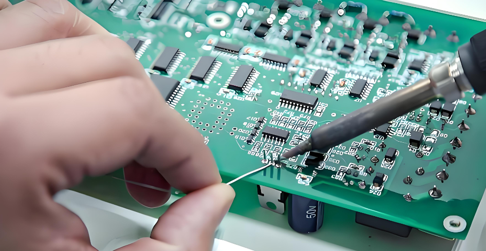
What Do Auditors and Medical OEMs Expect From OQ Documentation?
During audits or supplier qualification reviews, OQ documentation is often examined in detail. Auditors and OEMs typically expect to see:
- Clearly defined and justified process parameters
- Evidence that limits were intentionally challenged
- Repeatable and reproducible results
- Documented handling of deviations or anomalies
Well-structured OQ records demonstrate that the manufacturer understands its processes at an engineering level, rather than relying on empirical success alone.
How Does OQ Differ From IQ and PQ?
Although IQ, OQ, and PQ are closely related, each serves a distinct purpose:
- IQ confirms that equipment and systems are installed correctly
- OQ confirms that processes operate reliably within defined limits
- PQ confirms consistent output under normal production conditions
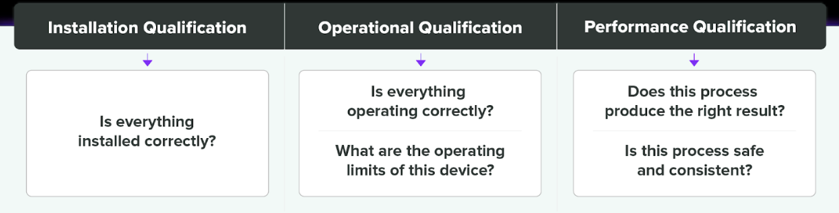
OQ acts as the bridge between installation and production, translating equipment capability into process control.
How Does (EBest Circuit) Best Technology Perform OQ for Medical PCBA Projects?
(EBest Circuit) Best Technology applies a structured OQ methodology tailored to medical electronics, including:
- Engineering-defined process limits
- Controlled variation during validation runs
- Comprehensive data collection and analysis
- Documentation aligned with ISO 13485 expectations
This approach ensures that medical PCBA assembly processes are not only functional, but technically understood and defensible.
What Comes After OQ in Medical PCBA Validation?
While OQ confirms that processes are capable, it does not yet prove long-term consistency in real production environments. That confirmation is provided by Performance Qualification (PQ), which evaluates routine manufacturing stability across multiple lots and operators.
Related reading:
Performance Qualification (PQ) in Medical PCBA Production
To fully understand how OQ fits within the complete validation framework, it is also recommended to review:
Installation Qualification (IQ) in Medical PCBA Manufacturing
Together, these stages form a comprehensive, regulator-accepted approach to medical PCBA process validation.