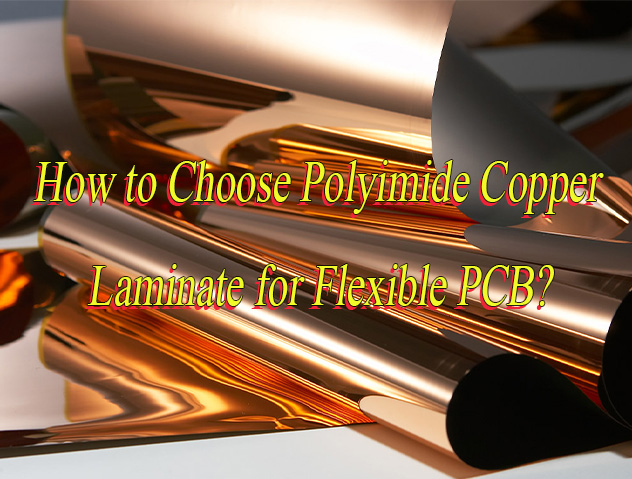
Why choose Polyimide copper laminate for flexible PCB? Let’s discover its definition, benefits, selection guide, spec, difference between adhesive-less and adhesive, common material supplier.
Are you troubled with these questions?
- Are you facing reliability issues in flexible circuits due to inadequate bend resistance of polyimide copper laminate?
- How to prevent high dielectric loss from compromising signal integrity during high-frequency signal transmission?
- How to achieve rapid delivery for small-batch, multi-variety orders while maintaining cost efficiency?
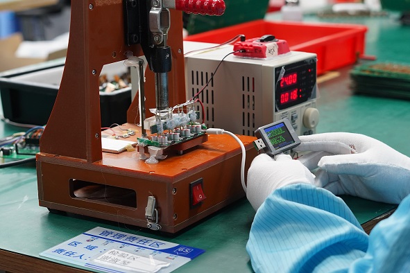
As a flexible PCB manufacturer, EBest Circuit (Best Technology) can provide you solution:
- Nano-modified PI substrate with gradient copper foil design achieves 200,000 crack-free cycles at 0.5mm bend radius, extending operational lifespan by 40%.
- Low-dielectric (Dk < 3.0) modified PI material combined with 3D microstrip line optimization reduces insertion loss by 20%, ensuring robust signal integrity during high-frequency transmission.
- Modular design and intelligent production scheduling enable 2-hour line changeovers, 72-hour global direct delivery, and maintain cost efficiency with only a 20% premium over mass production costs.
Welcome to contact us if you have any request for flexible PCB: sales@bestpcbs.com.
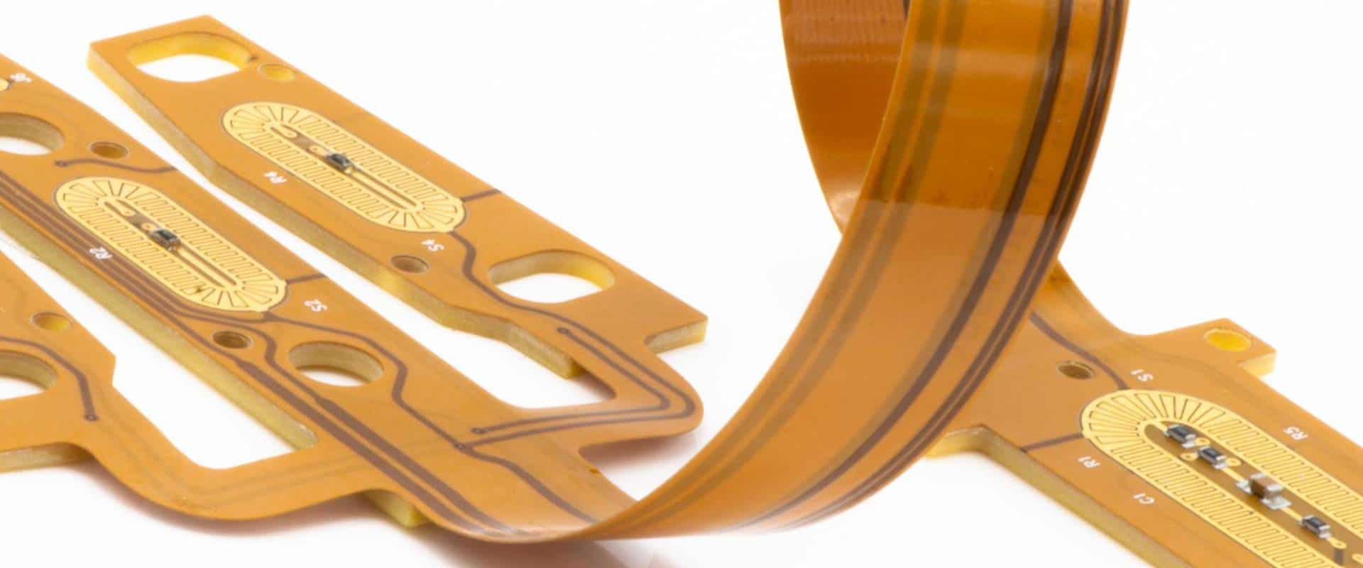
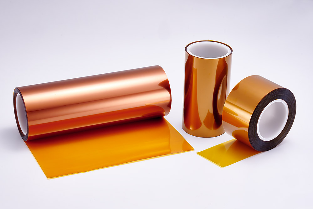
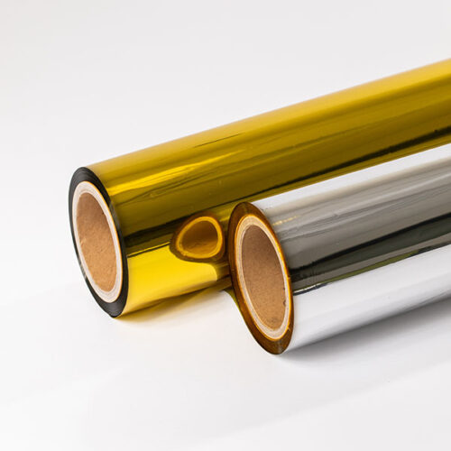
What Is Polyimide Copper Laminate?
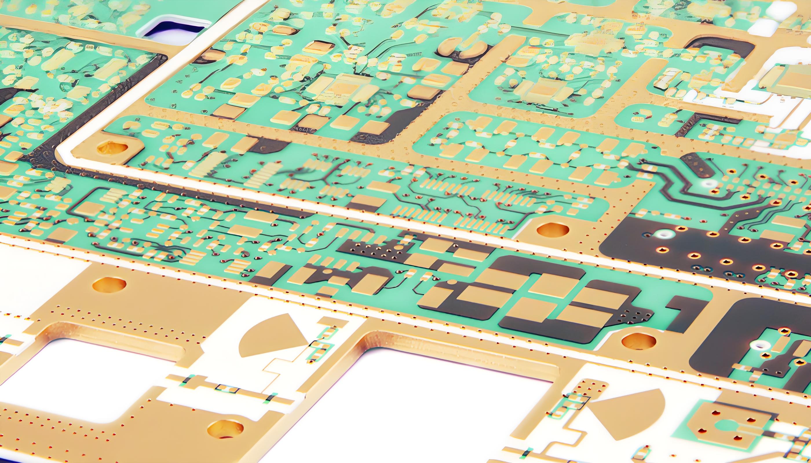
Polyimide Copper Laminate is a high-performance electronic substrate material composed of polyimide film (insulating substrate) and conductive copper foil, bonded through specialized processes such as high-temperature lamination or direct copper bonding techniques. Its core value lies in integrating polyimide’s extreme temperature resistance (capable of enduring prolonged exposure to temperatures above 260°C), exceptional flexibility (withstanding repeated bending), and copper foil’s superior electrical conductivity.
This combination makes it a critical foundational material for manufacturing flexible printed circuits (FPC) and high-temperature/high-frequency rigid circuit boards, particularly suited for demanding applications requiring both high-temperature stability and dynamic bending capabilities, such as smartphone foldable screens, aerospace electronics, and automotive engine compartment control units.
Why Choose Polyimide Copper Laminate for Flexible PCB?
Reasons why choose polyimide copper laminate for flexible PCB:
- Extreme Temperature Resistance: Withstands prolonged exposure above 260°C, ensuring stable operation in high-temperature environments like automotive engine compartments and aerospace electronics. Reduces equipment failure risks, maintenance costs, and downtime losses.
- Dynamic Flexibility Adaptation: Supports repeated bending, ideal for scenarios requiring frequent dynamic deformation (e.g., foldable smartphone screens, wearables). Enhances design freedom and space utilization while preventing circuit cracking from mechanical fatigue.
- Efficient Signal Transmission: Copper foil’s superior conductivity enables low-impedance, high-frequency signal transmission. Minimizes signal loss in 5G and high-frequency devices, improving response speed, accuracy, and end-product performance.
- Lightweight & Thin Design: Polyimide substrate’s lightweight, thin profile supports weight reduction and thinning of circuit boards. Suitable for portable devices (e.g., foldable smartphones) and spacecraft components, driving compact, portable product innovation.
- Chemical Stability: Corrosion-resistant and chemically inert properties maintain stability in harsh environments (e.g., high humidity, chemical pollution). Extends device lifespan by reducing environmental aging and long-term usage costs.
- Thermal Management Optimization: Good thermal conductivity aids heat dissipation, preventing performance degradation or component damage from localized overheating. Ensures stable operation in high-power computing and electronic devices.
- Process Compatibility: Highly compatible with existing flexible PCB manufacturing processes (e.g., high-temperature lamination, microvia processing). Reduces conversion barriers, shortens development cycles, and lowers technical transition risks/upfront investment.
- Long-Term Cost Efficiency: While initial material costs may be higher, its durability, fatigue resistance, and long lifespan reduce maintenance/replacement frequency. Saves hidden lifecycle costs and improves overall ROI.
How to Choose Polyimide Copper Laminate for Flexible PCB?
A guide to how to choose polyimide copper laminate for flexible PCB:
1. Precise Adaptation of Basic Parameters to Application Scenarios
- Thickness Stratification Design: Base material thickness must dynamically match bending radius, conventional flexible PCBs use 12.5-50μm PI; high-frequency applications (e.g., 5G antenna modules) prioritize 8-12μm ultra-thin PI to minimize signal loss; high-power scenarios (e.g., automotive power control modules) require 25-50μm thick PI for enhanced thermal stability.
- Copper Foil Type Selection: Electro-Deposited (ED) copper offers cost advantages for static or low-frequency bending scenarios; Rolled Annealed (RA) copper, with its dense grain structure, achieves >100,000 dynamic bending cycles, ideal for foldable smartphones and wearables.
- Mandatory Flame Retardancy Standards: Medical implants and automotive engine compartment electronics must meet UL94 V-0 flame retardancy to ensure safety redundancy in extreme environments.
2. Quantitative Validation of Thermal Performance Metrics
- Glass Transition Temperature (Tg) Grading: Conventional PI substrates have Tg ≥200°C for consumer electronics; industrial control modules require Tg >250°C specialty PI (e.g., DuPont Kapton® KJ series); aerospace applications near engines demand custom Tg >350°C materials.
- Coefficient of Thermal Expansion (CTE) Matching: X/Y-axis CTE must be controlled within 12-18ppm/°C to form a gradient match with copper foil (17ppm/°C), preventing interlayer delamination from thermal stress concentration.
3. High-Frequency Electrical Performance Optimization
- Low-Loss Dielectric Constant (Dk) Selection: High-frequency circuits (>1GHz) require Dk <3.0 PI-Cu materials like DuPont Pyralux AP or Ube Upilex-SA to reduce signal delay and loss.
- Volume Resistivity Reliability Verification: Humid environments (85°C/85% RH) must maintain >1×10¹⁶ Ω·cm, validated by ASTM D257 testing, ensuring long-term electrical insulation stability.
4. Dynamic Durability Testing of Mechanical Properties
- Standardized Peel Strength Verification: 1oz copper foil must achieve ≥0.8N/mm peel strength (IPC-6013 standard), validated via 90° peel testing for interfacial adhesion.
- Quantitative Bend Life Testing: Dynamic bending applications require ≥50,000 MIT fold cycles with a fold radius ≥3× material thickness; high-reliability scenarios (e.g., aerospace) demand >100,000 cycles.
5. Chemical Compatibility and Environmental Adaptability
- Full-Process Chemical Resistance Validation: Compatibility testing covers electroplating (copper/nickel sulfate), solder mask (epoxy/polyurethane), and other process chemicals to prevent material swelling or degradation.
- Moisture Absorption Control: Prefer hydrophobic modified PI (e.g., Mitsubishi Gas Neopulim®) with <0.8% moisture absorption to mitigate electrical performance drift in high-humidity environments.
6. Supplier Qualification and Batch Stability
- Full-Chain Certification Traceability: Suppliers must provide UL certification, ISO9001/14001 system certificates, and batch variation reports (±3% standard) for key parameters (Tg, CTE, peel strength) over six months.
- Supply Chain Risk Management: Prioritize suppliers with global delivery capabilities (e.g., DuPont, SABIC) and assess geopolitical risks impacting supply continuity.
7. Cost Optimization and Customization Strategies
- Stratified Cost Optimization: Non-critical layers (e.g., ground planes) may use low-Tg PI to reduce costs; high-frequency signal layers employ specialty low-loss PI for performance-cost balance.
- Bulk Customization Services: For orders >500m², negotiate custom solutions for copper foil thickness (e.g., 9μm/18μm), adhesive systems (acrylic/epoxy), and process requirements (e.g., laser microvia precision ±2μm).
Polyimide Copper Clad Laminate Specification
| Parameter | Typical Range/Value (with Units) |
| Substrate Type | Flexible (Adhesiveless/Adhesive-Coated), Rigid, High-Frequency Specialized |
| Total Thickness | 0.025–0.125 mm (Flexible), 0.2–3.2 mm (Rigid) |
| Copper Foil Thickness | 12–35 μm (0.5–1 oz) |
| Dielectric Constant (Dk) | 3.0–4.0 @1 GHz–10 GHz |
| Dissipation Factor (Df) | 0.002–0.025 @1 GHz–10 GHz (≤0.005 for high-frequency applications) |
| Glass Transition Temperature (Tg) | >250 °C (Flexible), >260 °C (Rigid) |
| Thermal Decomposition Temperature (Td) | >400 °C |
| Z-axis CTE | 20–70 ppm/°C (<Tg) |
| Peel Strength | ≥1.0 N/mm (Flexible), ≥1.5 N/mm (Rigid) |
| Water Absorption Rate | <0.5% (Flexible), <0.3% (Rigid) |
| Flame Retardancy Rating | UL94 V-0 |
| Dimensional Stability | ≤0.1% (MD/TD Directions) |
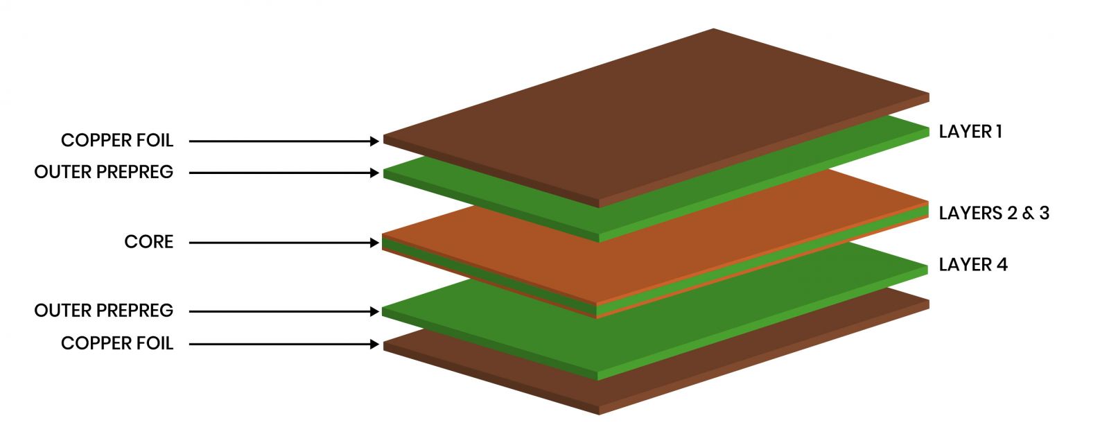
Difference between Adhesive-less vs. Adhesive Polyimide Copper Laminate
Structural Composition
- Adhesive-less Polyimide Copper Laminate(2L-FCCL): Composed of two layers, polyimide (PI) film directly bonded to copper foil without additional adhesive layers.
- Adhesive Polyimide Copper Laminate (3L-FCCL): Consists of three layers, PI film, organic adhesive (e.g., acrylic or epoxy resin), and copper foil.
Thermal Performance & Reliability
- Adhesive-less Polyimide Copper Laminate: Superior high-temperature resistance, thermal dimensional stability, and long-term reliability due to the absence of thermally inferior adhesive layers. Withstands harsh conditions like soldering above 300°C.
- Adhesive Polyimide Copper Laminate: Organic adhesive layers exhibit poorer thermal stability, softening or degrading above 150°C, leading to reduced peel strength and compromised reliability.
Thickness & Weight & Flexibility
- Adhesive-less Polyimide Copper Laminate: Thinner, lighter, and more flexible, ideal for dynamic bending applications and high-density wiring.
- Adhesive Polyimide Copper Laminate: Thicker and heavier due to adhesive layers, with reduced flexibility.
Electrical Performance
- Adhesive-less Polyimide Copper Laminate: Stable dielectric properties, lower dielectric loss, and better impedance control, suitable for high-frequency/high-speed applications.
- Adhesive Polyimide Copper Laminate: Adhesive layers may introduce additional dielectric loss and moisture absorption, potentially affecting electrical stability.
Peel Strength & Bonding Process
- Adhesive-less Polyimide Copper Laminate: Direct chemical bonding (e.g., coating, lamination, or sputtering) between copper and PI ensures high initial peel strength and stability at elevated temperatures. Requires high-purity PI films with excellent bonding properties.
- Adhesive Polyimide Copper Laminate: Relies on physical adhesion from adhesives, offering good peel strength at room temperature but significant degradation at high temperatures. Manufacturing processes are simpler and more mature.
Cost & Applications
- Adhesive-less Polyimide Copper Laminate: Higher cost due to complex manufacturing and stringent technical requirements. Used in high-end, high-reliability fields such as aerospace, military electronics, premium consumer electronics (foldable smartphones), automotive electronics, rigid-flex PCBs, and HDI boards.
- Adhesive Polyimide Copper Laminate: Lower cost and mature processes, widely applied in cost-sensitive, moderate-environment flexible circuits.
Dimensional Stability
- Adhesive-less Polyimide Copper Laminate: Lower coefficient of thermal expansion (CTE), minimizing dimensional changes during thermal cycling for high-precision circuits.
- Adhesive Polyimide Copper Laminate: Adhesive layers are prone to dimensional changes under heat, resulting in poorer overall stability.
Common Polyimide Copper Clad Laminate Supplier
DuPont (USA)
Products: Kapton® series polyimide film-based copper-clad laminates.
Advantages:
- Extreme temperature adaptability (-269°C to +400°C) for aerospace/automotive electronics; dielectic strength 3000–6000 V/mil, volume resistivity >10¹⁵ Ω·cm.
- Global supply chain with 40+ years’ experience, rapid delivery for large orders, and global technical support.
Rogers Corporation (USA)
Products: High-frequency/high-speed CCLs (RO3000, RO4000 series) and hybrid polyimide materials.
Advantages:
- Leading high-frequency performance (Dk 2.2–6.15, Df 0.001–0.004) for 5G/millimeter-wave radar; 50%+ global market share in RF/microwave, 60+ years’ expertise.
- Customizable hybrid designs (e.g., ceramic-filled PTFE) for multi-layer/hybrid circuits; UL-certified.
Kaneka (Japan)
Products: Apical® polyimide film and flexible CCL (FCCL).
Advantages:
- Ultra-thin film (7.5μm and below) for high-density flexible circuits (foldable phones/wearables); 80%+ global TPI market share for adhesive-free 2L FCCL.
- Stable Asian supply chain (Japan-based production) with short lead times.
Panasonic (Japan)
Products: High-speed CCLs (Megtron series) and polyimide-ceramic composites.
Advantages:
- Low loss (Df < 0.005) and stable Dk for servers/high-speed communication; advanced Dk control in high-temperature lamination.
- Halogen-free/RoHS compliance for EU/North American markets.
Isola (USA)
Products: High-performance CCLs (Astra MT77, TerraGreen series).
Advantages:
- Cost-effective high-frequency options (Dk 3.0, Df 0.0017) vs. Rogers; compatible with FR-4 processes for hybrid designs.
- Global production network (USA/Europe/Asia) for regional supply chain optimization.
Where Can I Buy a Reliable Polyimide Copper Laminate Board?
Professional B2B Procurement Platforms
- Alibaba International Station: Supports small-batch procurement (e.g., minimum order quantity of 10 square meters), provides integrated logistics and payment services, and allows screening of suppliers from Guangdong, Jiangsu, and other regions.
- Global Sources: Focuses on the electronics industry, supports free registration, allows listing of 100 products, and links with Hong Kong international exhibitions, suitable for professional buyers.
- Made-in-China.com: Covers over 3,500 product categories, supports 11 languages, accounts for 84% of overseas buyers, with an annual fee of CNY 31,100 for Audited Suppliers, ideal for SMEs.
International Certifications & Standard References
- UL Certifications: UL 796 (printed circuit substrates) and UL 94 (flame retardancy, e.g., V-0 rating) ensure material safety and electrical performance.
- ISO Systems: ISO 9001 (quality management), RoHS (environmental compliance), and REACH (chemical safety) guarantee regulatory compliance in production.
- Chinese National Standard GB/T 16315-2017: Specifies electrical, thermal (glass transition temperature ≥200°C), and mechanical (peel strength ≥60N) performance for copper-clad polyimide glass fabric laminates.
Logistics & Customs Clearance Services
- Logistics Options: Select air freight (fast), sea freight (cost-effective), or international couriers (e.g., DHL, FedEx) based on volume, weight, and delivery time. High-value shipments are recommended for air/express with transport insurance.
- Customs Documents: Prepare invoices, packing lists, certificates of origin, UL/ISO certification files, and comply with destination country requirements (e.g., Russia/Ukraine’s lenient air clearance, Africa’s “gray customs” risks).
- Overseas Warehousing: Moscow (Russia) and Almaty (Kazakhstan) overseas warehouses support local clearance and dropshipping, suitable for e-commerce and bulk orders.
Payment & After-Sales Guarantees
- Payment Methods: Telegraphic Transfer (TT), Letter of Credit (LC), third-party platforms (PayPal, Western Union), and Open Account (OA) terms, chosen based on transaction value, country risk, and supplier requirements.
- After-Sales Support: Confirm suppliers offer technical support, return/replacement policies, and long-term supply capabilities. Contracts must specify quality standards, delivery timelines, liability clauses, and dispute resolution (e.g., international arbitration).
Industry Resources & Expansion Channels
- Exhibitions & Associations: Participate in China Electronics Fair (CEF) and International Electronics Circuit Exhibition (CPCA) for direct supplier engagement and technology updates.
- Technical Forums: Utilize platforms like Zhihu and Guide Chemical Network Community for peer insights and supplier reviews.
- Customs & Logistics Advisory: Monitor destination country regulations (e.g., EU CE certification, U.S. FCC compliance) and logistics timelines to plan shipments proactively.
Welcome to contact us if you have any other issues about Polyimide copper laminate: sales@bestpcbs.com.