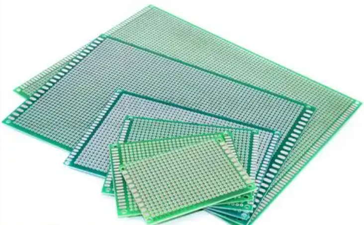
Single sided PCB is one of the most practical board types for straightforward electronic designs. With copper circuitry on only one side of the substrate, it offers a simple structure, stable performance, and competitive manufacturing cost for high-volume applications.
At EBest Circuit, we provide custom single sided PCB manufacturing for customers who need dependable quality, fast turnaround, and responsive engineering support. From prototype runs to volume production, our team helps you move from design to delivery with better efficiency and fewer production concerns.
What Is a Single Sided PCB?
A single sided PCB, also called a 1 layer PCB, is a printed circuit board with conductive copper traces on only one side of the substrate. All components are mounted on the same side, and the electrical paths are routed through a single copper layer.
This is one of the most basic and widely used PCB structures in electronics. Because of its simple layout and efficient production process, a single sided PCB is often chosen for products that do not require complex routing or high component density.
In most cases, the base material is FR4 or another insulating substrate, with a copper foil laminated on one side. The copper is then etched to form the required circuit pattern.
Single sided PCBs are commonly used in:
- LED lighting products
- Power supplies
- Consumer electronics
- Calculators
- Simple control boards
- Household appliances
For straightforward electronic designs, this board type remains a practical and cost-efficient solution.
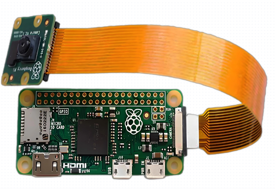
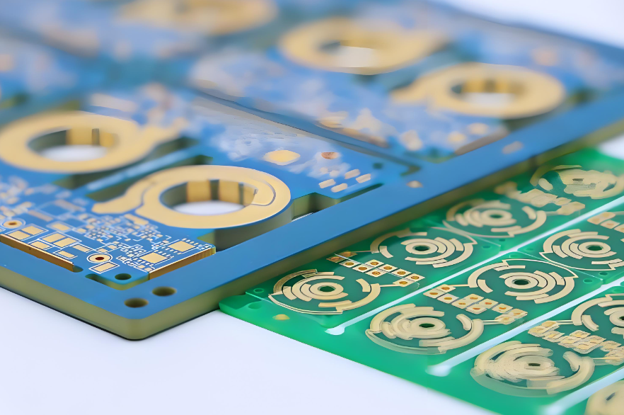
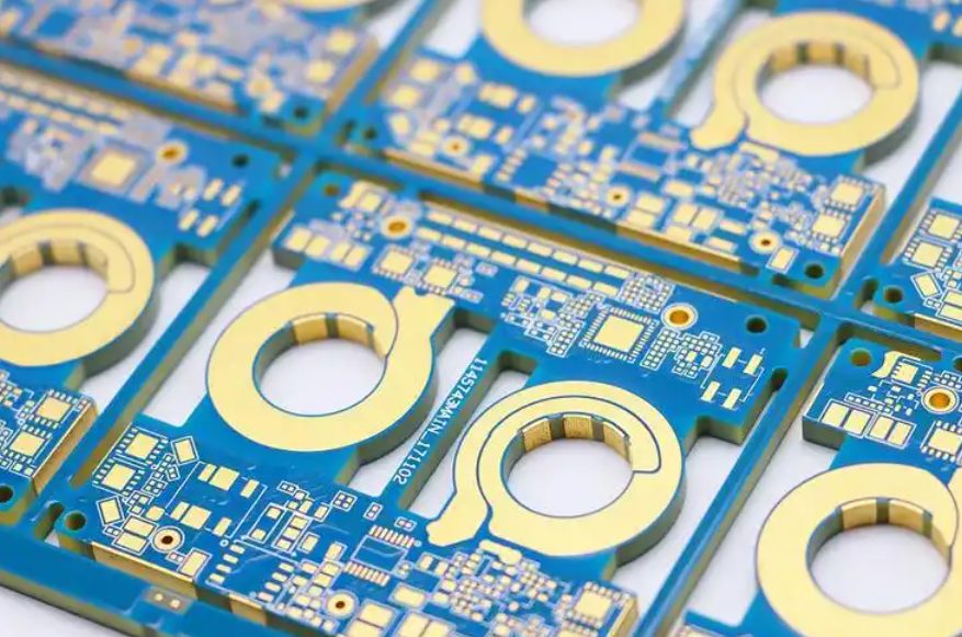
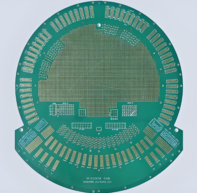
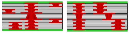
Single Sided PCB
Our Single Sided PCB Manufacturing Capabilities
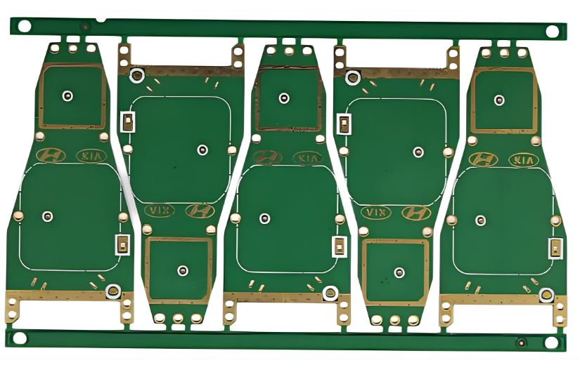
At EBest Circuit, we support custom PCB manufacturing with a strong focus on manufacturability, quality consistency, and customer-specific requirements. Our single sided PCB service is suitable for both basic commercial products and more specialized industrial applications.
Available Options Include:
- Custom board dimensions
- FR4 and other substrate selections
- Different copper thickness options
- Multiple solder mask colors
- Surface finishes based on assembly and performance needs
- Prototype, small batch, and mass production support
- Through-hole and SMT compatible designs
We review each project based on the intended application, assembly method, and electrical requirements, helping customers choose a more suitable board configuration before production starts.
How Is a Single Sided PCB Manufactured?
The manufacturing process of a single sided PCB is relatively direct, which is one reason it remains popular for high-volume production and cost-sensitive projects.
1. Circuit Design and Layout
The process starts with PCB design. Engineers create the circuit layout using CAD software, defining component placement, trace routing, hole positions, and board dimensions.
A clean layout is especially important in a 1 layer PCB because routing space is limited. Good design at this stage helps reduce manufacturing risk and improves final board performance.
2. Substrate Preparation
After the design is finalized, the insulating substrate is prepared and cut to the required board size. FR4 is one of the most common materials used, although other substrates may be selected depending on the application.
3. Copper Lamination
A thin copper layer is laminated onto one side of the substrate. This copper layer will later be patterned into the conductive traces needed for the circuit.
4. Photoresist Coating
A light-sensitive photoresist material is applied over the copper surface. This coating protects the intended circuit pattern during the etching stage.
5. Exposure and Development
The board is exposed to UV light through a film or mask containing the circuit image. After development, the unwanted photoresist is removed, leaving the desired copper pattern protected.
6. Etching
The exposed copper is removed through a chemical etching process. Only the protected copper remains, creating the final conductive pathways.
7. Solder Mask Application
A solder mask is applied over the board surface to protect the copper traces from oxidation and reduce the risk of solder bridging during assembly. Green is the most common color, though other colors are also available.
8. Component Assembly and Soldering
Electronic components are mounted in their designated positions. Depending on the design, this may involve SMT assembly or through-hole soldering.
9. Testing and Inspection
The finished board goes through electrical testing and quality inspection to confirm continuity, functionality, and manufacturing accuracy. This step helps ensure the PCB performs as designed before shipment.
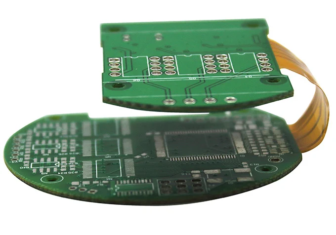
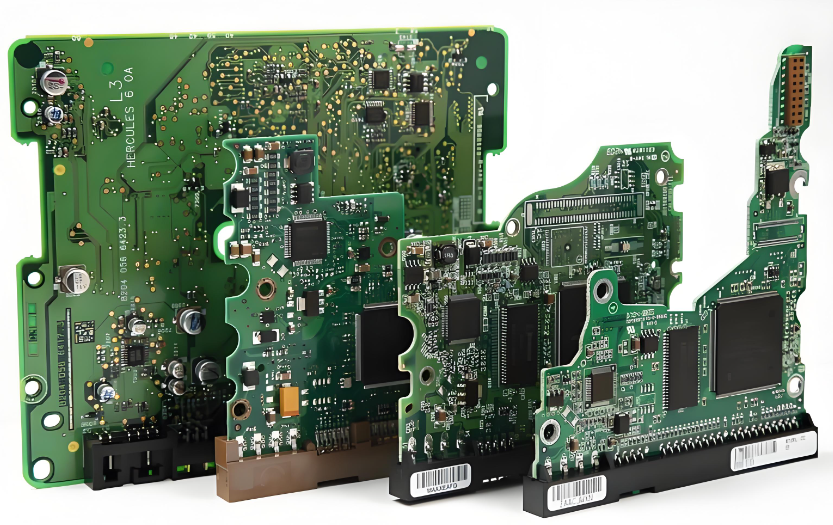
What Is a Double Sided PCB?
A double sided PCB has conductive copper layers on both sides of the substrate. This structure allows components and traces to be placed on the top and bottom surfaces, giving designers more routing flexibility.
To connect the two copper layers, the board uses plated through holes (PTH) or vias. These conductive holes allow electrical signals to move from one side of the board to the other.
Because of this added routing capability, double sided PCBs are suitable for more complex circuits than single sided boards. They are widely used in:
- Automotive electronics
- Communication equipment
- Industrial control systems
- Power electronics
- Instrumentation devices
A double sided PCB is often the next step when a single-layer layout can no longer support the required circuit density.
What Is a Double Sided PCB?
Single Sided PCB vs Double Sided PCB
Choosing the right board type depends on circuit complexity, layout density, and budget expectations. For many buyers, the first comparison is between single sided PCB and double sided PCB.
| Item | Single Sided PCB | Double Sided PCB |
| Copper Layers | 1 | 2 |
| Circuit Complexity | Low | Medium |
| Routing Flexibility | Limited | Higher |
| Manufacturing Cost | Lower | Higher |
| Production Process | Simpler | More complex |
| Through Hole Connection | Not required for interlayer routing | Required for layer connection |
| Typical Applications | Simple electronics | More compact and functional products |
If the layout can be completed on one layer without excessive jumpers or routing compromise, single sided PCB is usually the more economical option. When routing space becomes tight, double sided PCB offers greater design freedom.
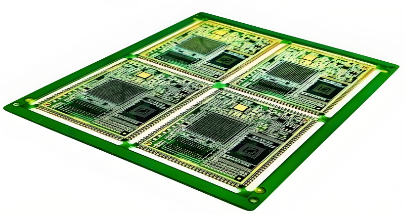
Single Sided PCB vs Multilayer PCB
A multilayer PCB includes three or more conductive layers and is built for more advanced circuits. Compared with a 1 layer PCB, it supports higher density routing, better signal management, and more compact product design. However, many products do not need that level of complexity.
A single sided PCB is usually the better fit when you need:
- A cost-sensitive board solution
- Simple electrical architecture
- Faster production
- Easier inspection and assembly
- Stable supply for repetitive orders
A multilayer PCB is more appropriate when the project involves:
- High-speed signal routing
- Compact board area with dense components
- Strict EMI or impedance requirements
- More advanced system integration
The best choice is not always the most complex structure. It is the one that matches your product’s real design needs.
Single Sided PCB vs Multilayer PCB
How Thick Is a Single Sided PCB?
The thickness of a single sided PCB depends on the application, mechanical requirements, and manufacturing specification. In many cases, the common finished thickness range is:
- 0.6 mm
- 0.8 mm
- 1.0 mm
- 1.2 mm
- 1.6 mm
Among these, 0.8 mm to 1.0 mm is often selected for standard applications because it provides a good balance between strength, weight, and cost.
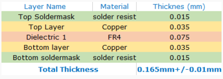
PCB thickness usually includes:
- Base substrate thickness
- Copper thickness
- Solder mask and surface finish contribution
Thicker boards may be preferred when stronger mechanical support is needed. Thinner boards may be selected for compact or lightweight products.
Choosing the right board thickness should always be based on the end-use environment, assembly method, and overall design requirements.
How to Choose the Right PCB Type for Your Project?
Selecting between a single sided PCB, double sided PCB, and multilayer PCB depends on several practical factors.
Choose a Single Sided PCB If:
- Your circuit is simple
- Cost control is a priority
- Component density is low
- Fast fabrication is important
- The product is mature and stable
Choose a Double Sided PCB If:
- You need more routing space
- Components must be mounted on both sides
- A single-layer layout becomes too crowded
- The product requires moderate complexity
Choose a Multilayer PCB If:
- The design includes complex signal routing
- Space is limited
- High-speed or high-performance performance matters
- EMI control and signal integrity are critical
A good PCB supplier can review your files and recommend the most suitable stack-up and board type before production begins.
Common Applications of Single Sided PCB
Single sided PCBs are still widely used across many industries because they serve a large number of standard electronic functions efficiently.
Typical applications include:
- LED modules and lighting controls
- AC/DC power boards
- Battery management in simple devices
- Consumer appliance boards
- Small motor control circuits
- Basic sensor and interface boards
- Chargers and adapters
- Industrial support electronics
For buyers looking for a dependable and cost-conscious board platform, this type of PCB remains highly relevant.
What Files Do We Need for Quotation?
To provide an accurate quotation and technical review, it is helpful to share:
- Gerber files
- Drill files
- PCB specification details
- Board size and thickness
- Copper thickness requirement
- Surface finish requirement
- Quantity demand
- Assembly files if PCBA is needed
If your files are still under preparation, you can also send the available design information first. Our team can help review the project and advise on the next step.
Get a Quote for Single Sided PCB Manufacturing
Looking for a reliable single sided PCB manufacturer for your next project?
EBest Circuit supports custom 1 layer PCB fabrication with responsive engineering service, practical lead times, and dependable production quality. Whether you need a quick prototype or a stable supplier for volume orders, we are ready to support your project.
Send us your design files and specifications for a fast review and quotation.
Email: sales@bestpcbs.com