Is RO4835 material the right laminate for your next high frequency PCB project? In RF, radar, microwave, antenna, and communication circuits, the PCB substrate has a direct influence on signal loss, impedance stability, phase behavior, and long-term reliability.
Compared with standard FR4, this Rogers laminate offers lower loss, stable dielectric behavior, and improved oxidation resistance. It is also easier to process than many traditional microwave laminates, making it a practical option for projects that need both RF performance and efficient production.
This guide explains its key properties, selection points, manufacturing process, LoPro option, and supplier considerations for high frequency PCB manufacturing.
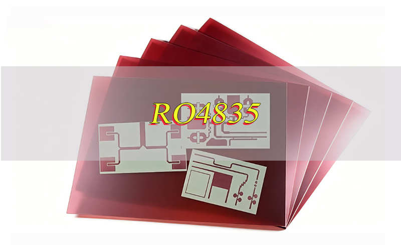
What Is RO4835 Material?
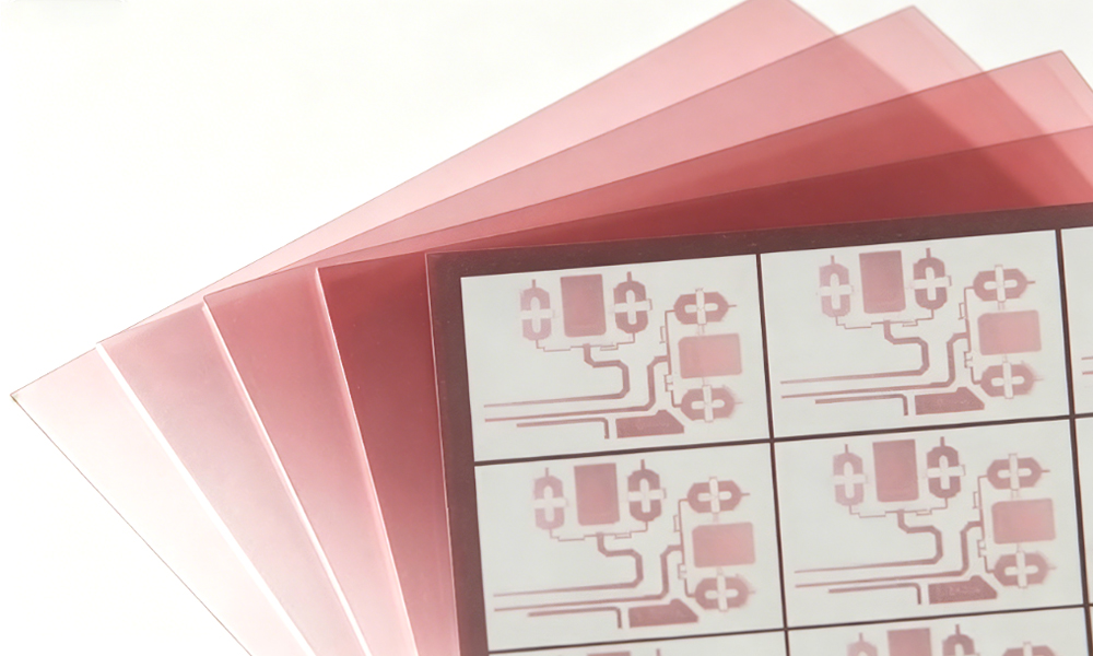
RO4835 material is a high frequency circuit laminate from the Rogers RO4000 series. It is designed for RF, microwave, radar, sensor, antenna, and controlled impedance PCB applications where stable electrical performance is required.
Unlike standard FR4, it uses a hydrocarbon ceramic-filled system. This structure gives the laminate a strong balance of low loss, thermal stability, dimensional consistency, and standard PCB process compatibility.
For many high frequency PCB projects, material choice affects:
- Impedance control
- Insertion loss
- Phase stability
- Soldering reliability
- Long-term service life
In simple terms, this laminate is selected when FR4 cannot provide enough RF consistency, but the product still needs a material that supports efficient PCB manufacturing.
Why Is RO4835 Used in High Frequency PCB Designs?
This laminate is used in high frequency PCB designs because it provides stable dielectric properties, low signal loss, good thermal behavior, and improved oxidation resistance. These features help the board maintain consistent signal performance in RF and microwave circuits.
At lower frequencies, the PCB substrate may not strongly affect the signal. However, as the operating frequency increases, the laminate becomes part of the signal path. The dielectric constant, dissipation factor, copper roughness, trace geometry, and stackup all influence the final result.
Benefits for high frequency PCB designs:
- Helps maintain controlled impedance.
- Reduces dielectric loss compared with ordinary FR4.
- Supports better phase consistency.
- Helps antenna and RF circuits stay closer to the target frequency.
- Provides better long-term reliability in warmer operating environments.
- Works with many standard PCB fabrication methods.
That is why this material is often considered when a project needs stronger RF performance than FR4 while still requiring a practical manufacturing route.
What Is the Dielectric Constant of RO4835?
The dielectric constant of RO4835 is typically 3.48 ± 0.05 at 10 GHz as a process Dk. Its design Dk is commonly listed as 3.66 from 8 GHz to 40 GHz. For 4 mil laminates, the process Dk is usually 3.33 ± 0.05.
Dielectric constant, also called Dk, describes how the PCB laminate stores electrical energy in an electromagnetic field. In high frequency PCB design, this value directly affects signal speed, wavelength, impedance, and resonance behavior.
It is also important to distinguish between process Dk and design Dk. Process Dk is measured under standard test conditions and is often used for material comparison. Design Dk is more useful for circuit modeling because it better reflects practical PCB performance.
For RF, microwave, antenna, and radar circuits, a stable Dk helps the circuit maintain predictable electrical behavior across the target frequency range. This is one of the key reasons RO4835 is selected for high frequency PCB applications.
What Are RO4835 Tan Delta and Loss Performance?
Its typical dissipation factor, also called tan delta or Df, is 0.0037 at 10 GHz. This low-loss characteristic makes the laminate suitable for RF and microwave PCB applications.
Tan delta shows how much signal energy is lost in the dielectric material. A lower value usually means lower dielectric loss, cleaner signal transmission, and better high frequency behavior.
However, total PCB loss does not depend on the laminate alone. It is also affected by copper roughness, trace length, trace width, via transition, surface finish, and final stackup.
| Factor | Influence on Performance |
|---|---|
| Dissipation factor | Affects dielectric loss |
| Copper roughness | Affects conductor loss |
| Trace geometry | Influences impedance and insertion loss |
| Via transition | Impacts return loss and signal continuity |
| Surface finish | May affect RF loss at higher frequencies |
| Etching accuracy | Controls final trace width |
| Stackup consistency | Supports stable signal behavior |
For high frequency PCB manufacturing, the material gives a reliable foundation. Still, the final board performance also depends on controlled fabrication, proper stackup design, and accurate process execution.
What Does the RO4835 Datasheet Indicate?
The datasheet shows that this laminate is designed for high frequency circuit applications. It offers low loss, stable dielectric constant, low moisture absorption, good thermal stability, and improved oxidation resistance.
| Property | Typical Value |
|---|---|
| Process Dk | 3.48 ± 0.05 at 10 GHz |
| Design Dk | 3.66 from 8–40 GHz |
| Dissipation factor | 0.0037 at 10 GHz |
| Thermal coefficient of Dk | +50 ppm/°C |
| Decomposition temperature | 390°C |
| Glass transition temperature | >280°C |
| Z-axis CTE | 31 ppm/°C |
| Thermal conductivity | 0.66 W/m·K |
| Moisture absorption | 0.05% |
| Flammability | UL 94 V-0 |
| Lead-free process compatibility | Yes |
The datasheet helps confirm available laminate thicknesses, copper options, panel sizes, and process compatibility. For RF and microwave PCBs, these details should be checked before layout finalization and production.
RO4835 vs RO4350B: What Is the Difference?
RO4835 and RO4350B are both high frequency laminates from the Rogers RO4000 series. They share similar electrical properties and are widely used for RF, microwave, radar, antenna, and communication circuit boards.
The main difference is that RO4835 offers improved oxidation resistance. This makes it a good option for applications that may experience higher operating temperatures, longer service life, or more demanding environmental conditions.
| Item | RO4835 | RO4350B |
|---|---|---|
| Material family | RO4000 series | RO4000 series |
| Process Dk | 3.48 ± 0.05 | 3.48 ± 0.05 |
| Dissipation factor | 0.0037 at 10 GHz | 0.0037 at 10 GHz |
| Design Dk | 3.66 | 3.66 |
| Processing method | Similar to standard PCB processes | Similar to standard PCB processes |
| Key advantage | Improved oxidation resistance | Mature and widely used RF laminate |
| Suitable uses | Radar, sensors, high-reliability RF boards | RF modules, antennas, amplifiers, microwave boards |
RO4350B is a mature and common choice for many RF PCB projects. The other option is often selected when the board needs extra long-term thermal stability and improved resistance to oxidation.
Therefore, the choice depends on application conditions. If the PCB will be used in automotive radar, sensor systems, or higher-temperature RF environments, the oxidation-resistant option may offer a stronger reliability margin.
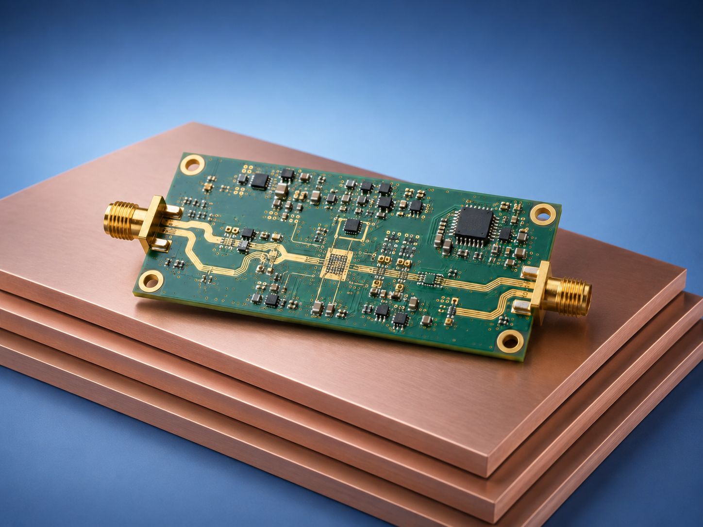
When Should You Choose RO4835 High Frequency PCB?
You should choose this high frequency PCB material when your circuit needs low loss, stable impedance, controlled dielectric behavior, and better reliability than standard FR4 can provide. It is especially suitable for the following PCB projects:
- Automotive Radar and Sensor Boards: Radar circuits require stable signal transmission, accurate impedance, and reliable performance over time.
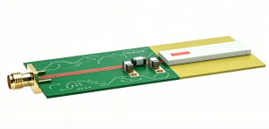
- RF Communication Modules: RF modules often need stable transmission lines, matching networks, filters, and antenna feed structures.
- Microwave Circuit: At microwave frequencies, material loss and dielectric variation become more critical.
- Power Amplifier Boards: Power amplifier circuits need stable electrical performance and good thermal behavior.
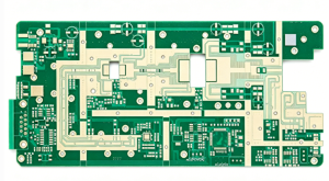
- Controlled Impedance Multilayer PCBs: The laminate can be used in multilayer and hybrid stackups. However, the stackup must be reviewed carefully to control impedance and lamination quality.
Before choosing this material, it is helpful to check:
- Operating frequency
- Signal loss requirement
- Target impedance
- PCB layer count
- Copper thickness
- Surface finish
- Application temperature
- Production quantity
- Testing requirements
- Reliability requirements
It is a good material choice when stable RF performance and long-term reliability are more important than the lowest material cost.
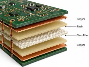
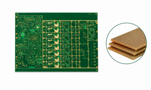
How Is RO4835 High Frequency PCB Manufactured?
High frequency PCB manufacturing requires tighter process control than standard FR4 PCB fabrication. For RF, microwave, radar, and antenna circuits, small changes in line width, dielectric thickness, copper thickness, or plating quality may affect impedance and signal performance. Therefore, each production step should be carefully reviewed and controlled.
1. Material Confirmation
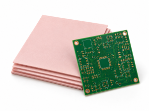
- The first step is to confirm the laminate type, material thickness, copper weight, panel size, and batch information. This helps ensure that the selected laminate matches the approved stackup and customer specification. Batch information is also important for production traceability, especially for RF and high-reliability PCB projects.
2. Stackup Review
- Before production starts, the stackup should be reviewed according to impedance requirements, dielectric thickness, copper thickness, layer count, and reference layer structure. This step helps confirm whether the trace width and spacing can meet the target impedance. A clear stackup review can also reduce production risk before fabrication begins.
3. Inner Layer Imaging and Etching
- During inner layer imaging, the circuit pattern is transferred onto the copper surface. After that, the unwanted copper is removed through etching. For high frequency circuits, line width control is especially important because even a small deviation may affect impedance, insertion loss, and signal consistency. Clean imaging and stable etching help maintain accurate RF trace geometry.
4. Lamination
- In multilayer PCB production, the inner layers are bonded together through lamination. Pressure, temperature, bonding material, heating rate, and cooling rate should be properly controlled. Good lamination helps maintain board flatness, dielectric consistency, and layer-to-layer alignment. For hybrid stackups, material compatibility should also be reviewed before production.
5. Drilling
- Drilling creates through holes, vias, and mounting holes according to the design files. Suitable drill tools, spindle speed, feed rate, and backup materials should be selected to achieve clean hole walls. Good drilling quality supports reliable plating and helps reduce defects such as rough hole walls, smear, burrs, and hole position deviation.
6. Hole Treatment and Metallization
- After drilling, the hole walls need to be cleaned and prepared for copper deposition. This process helps remove drilling residue and improves copper adhesion inside the holes. Stable hole treatment is important for plated through-hole reliability, especially in multilayer boards where electrical connection between layers must remain consistent.
7. Copper Plating
- Copper plating builds the required copper thickness on the hole walls and board surface. Uniform plating helps improve conductivity, mechanical strength, and long-term reliability. For high frequency boards, plating control should be stable because excessive or uneven copper may influence final trace dimensions and impedance performance.
8. Outer Layer Imaging and Etching
- The outer layer circuit pattern is then formed through imaging and etching. Accurate RF trace width, smooth copper edges, and controlled spacing are important at this stage. Since high frequency signals are sensitive to conductor geometry, outer layer etching should be carefully controlled to keep the final circuit close to the designed values.
9. Surface Finish
- Surface finish protects exposed copper and improves solderability during assembly. Common options include ENIG, OSP, HASL, and other finishes depending on project requirements. For RF applications, the surface finish should be selected based on solderability, shelf life, assembly process, frequency range, and possible influence on signal loss.
10. Inspection and Testing
- Final inspection confirms whether the PCB meets drawing, electrical, and quality requirements. Common checks include AOI, electrical testing, impedance testing, dimensional inspection, visual inspection, and hole quality inspection. For critical RF boards, test coupons may also be used to verify impedance performance before shipment.
This Rogers laminate is easier to process than many PTFE-based microwave materials, but high frequency PCB production still requires careful process control. The final result depends on both material quality and manufacturing accuracy.
Why Choose EBest for RO4835 PCB Manufacturing?
EBest supports high frequency PCB manufacturing with practical production experience and one-stop service from PCB fabrication to PCBA assembly. Here are reasons why choose EBest for RO4835 PCB manufacturing:
- Laminate selection support: We help customers review laminate thickness, copper weight, stackup structure, and application requirements before production.
- High frequency PCB manufacturing capability: We support RF, microwave, radar, sensor, antenna, communication, and controlled impedance PCB projects.
- Controlled impedance PCB support: We can assist with impedance stackup review, trace width control, impedance coupon planning, and production testing.
- Free DFM review before production: We check manufacturability details such as trace width, spacing, via structure, copper balance, drilling, surface finish, and panel design.
- Multilayer and hybrid stackup production: We support multilayer PCB and hybrid PCB structures based on project requirements.
- Prototype and small-batch manufacturing: We help customers move from sample verification to stable production with flexible order support.
- Turnkey PCBA assembly service: In addition to PCB fabrication, we can provide component sourcing, SMT assembly, DIP assembly, testing, and final inspection.
- Reliable component sourcing: We help customers source suitable components for RF, communication, industrial, automotive, medical, and control applications.
- Quality inspection and testing: Our quality process can include AOI, X-ray inspection, electrical testing, impedance testing, functional testing, and final quality checks.
- Traceability support: We provide production traceability for material, process, inspection, and shipment records.
- Support for demanding industries: EBest serves customers in communication, industrial control, automotive electronics, medical devices, aerospace/UAV, RF modules, and high-performance electronics.
For high frequency PCB projects using Rogers materials, EBest can help customers reduce design-to-production risk, improve production consistency, and build reliable RF circuit boards from prototype to volume production.
FAQs About RO4835 Material
Q1: What does RO4835 LoPro mean?
A1: RO4835 LoPro refers to a laminate option using low-profile copper. Low-profile copper can help reduce conductor loss at higher frequencies, especially when the circuit has long RF traces, tight insertion loss targets, or sensitive phase requirements.
Q2: When should I choose RO4835 LoPro instead of standard copper?
A2: Choose the LoPro option when conductor loss is a major concern. It is especially useful for microwave circuits, radar boards, antenna feed lines, and high-speed RF transmission paths where copper surface roughness may affect signal quality.
Q3: Can this laminate replace FR4 in every high frequency PCB?
A3: Not always. It is a better fit when the circuit needs low loss, stable impedance, and reliable RF behavior. For simple low-frequency boards, FR4 may still be more economical.
Q4: Is this material suitable for lead-free assembly?
A4: Yes. Its high thermal stability helps the board withstand common lead-free reflow and soldering processes.
Q5: Can it be combined with FR4 in one multilayer PCB?
A5: Yes. It can be used in hybrid multilayer PCB structures. However, the stackup, bonding material, lamination cycle, and thermal expansion behavior should be checked before production.
Q6: What files are needed for a quotation?
A6: A complete quotation usually requires Gerber files, drill files, stackup information, copper thickness, surface finish, board thickness, impedance requirements, quantity, and assembly details if PCBA service is needed.
Q7: How can EBest help with this type of PCB project?
A7: EBest can support material review, DFM checking, controlled impedance production, PCB fabrication, component sourcing, PCBA assembly, inspection, testing, and production traceability.
Contact Us for Custom High Frequency PCB Quotation
Looking for a reliable manufacturing partner for your high-frequency PCBs? EBest helps you reduce production risk with material selection support, controlled impedance review, DFM feedback, precise fabrication, and one-stop PCBA assembly.
Whether your project involves RF modules, radar boards, microwave circuits, antenna PCBs, or communication equipment, our team can help you move from prototype to production with better consistency and fewer delays.
Send your Gerber files, stackup requirements, quantity, and technical notes to sales@bestpcbs.com today. We will review your project and provide a fast, practical quotation for your high-frequency PCB needs.