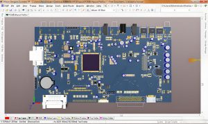
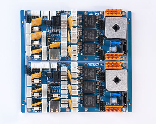
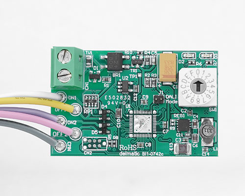
Automatic test equipment (ATE) plays a vital role in the field of electronic manufacturing, especially in the testing of printed circuit board assemblies (PCBA). In order to ensure the quality of PCBA, automatic test equipment (ATE) has become an indispensable force in the PCBA testing process with its high efficiency, accuracy and reliability.
What are the 7 types of PCB testing methods?
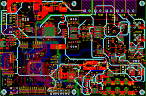
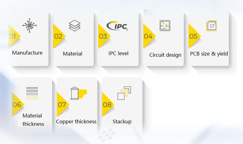
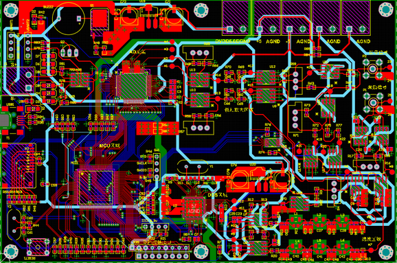
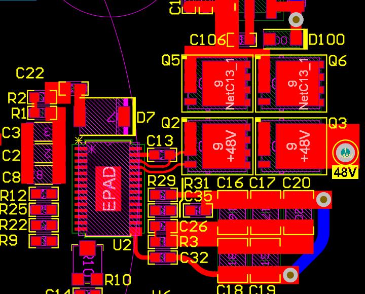
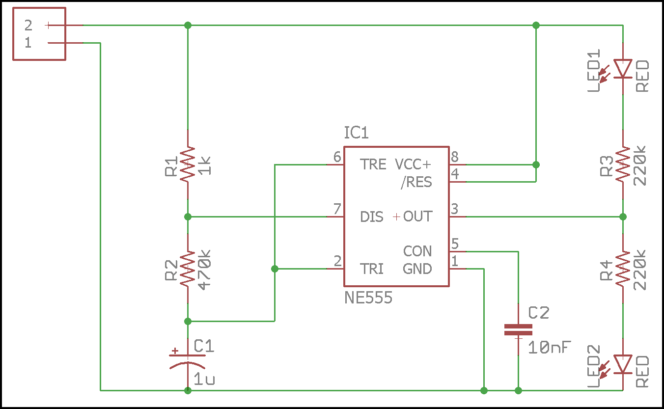
The common detection methods of PCB (Printed Circuit Board) boards are mainly used to detect the quality and accuracy of PCB boards, which is an indispensable part of the PCB production process. The following are 7 commonly used PCB board detection methods:
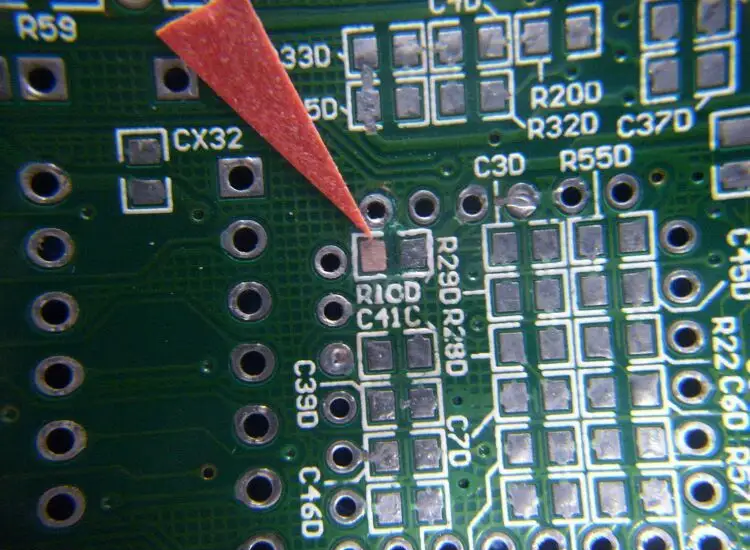
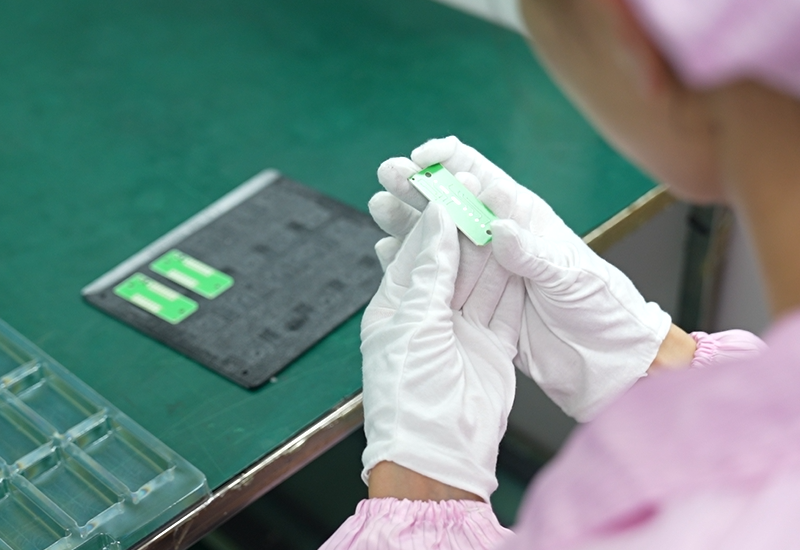
- 1. Visual inspection: Visual inspection is the simplest detection method. It observes the surface of the PCB board with human eyes to find possible defects, such as welding problems, component position offset, etc.
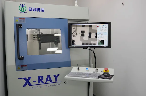
- 2. X-ray detection: X-ray detection is mainly used to detect problems hidden inside the PCB board, such as welding quality, BGA ball welding quality, inner layer line routing problems, etc.
- 3. Non-destructive testing: Non-destructive testing is a non-destructive detection method. Commonly used technologies include infrared testing, ultrasonic testing and electromagnetic wave testing.
- 4. AOl (Automated Optical Inspection): AOl is a method of automated inspection using optical equipment, which detects problems on the surface of PCB boards through high-resolution camera systems and pattern recognition software.
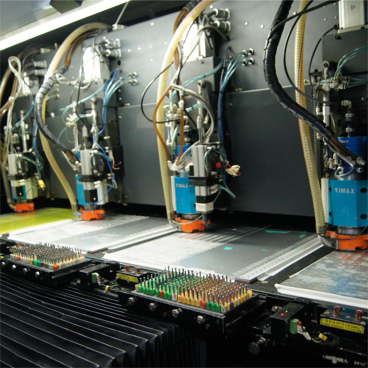
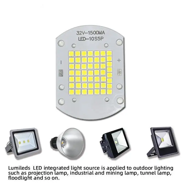
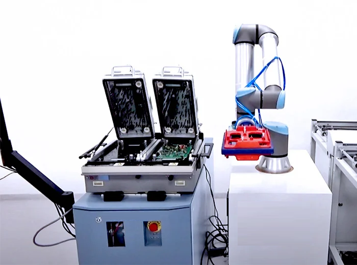
- 5. ATE (Automatic Test Equipment): ATE is an automatic test equipment used to test the electrical performance and functions of PCB boards.
- 6. Vibration test: Vibration test is used to detect the reliability and durability of PCB boards in vibration environments. By applying vibrations of different frequencies and amplitudes, the problems that may occur in actual use of PCB boards can be evaluated.
- 7. Thermal shock test: Thermal shock test is used to detect the performance of PCB boards in temperature change environments. By rapidly changing the temperature, the thermal expansion, thermal stability and welding quality of PCB boards can be evaluated.
These methods can comprehensively evaluate the quality and performance of PCB boards and detect potential problems in a timely manner to ensure the reliability and stability of PCB boards.
What is ate testing in semiconductor?
ATE testing is an important link in the semiconductor industry for testing the functional integrity and reliability of integrated circuits (ICs). It is the abbreviation of Automatic Test Equipment, which is a device that tests devices, circuit boards, and subsystems through computer control.
ATE testing plays a vital role in the semiconductor manufacturing process. It is a key step to ensure the quality of IC products. The test content includes DC parameter testing, AC parameter testing, functional testing, etc. These tests are designed to evaluate the performance, function, and reliability of the chip.
The basic principle of the test is to apply stimulus to the chip through the test vector, measure the response output of the chip, and compare it with the expected result to determine whether the chip meets the specification requirements.
ATE testing not only involves testing various parameters of the chip, but also includes structural testing of the chip, that is, detecting manufacturing defects to ensure the quality and reliability of the chip.
In addition, ATE testing also includes testing of voltage, current, frequency, pulse, temperature and other aspects of the chip to achieve comprehensive testing of the static parameters and dynamic performance of semiconductor chips.
In general, ATE testing is an important means of quality control of integrated circuits in the semiconductor industry. It improves the efficiency and accuracy of testing through automation, ensures the quality and reliability of semiconductor chips, and is an indispensable and important link in the semiconductor manufacturing process.
What is an ATE PSU?
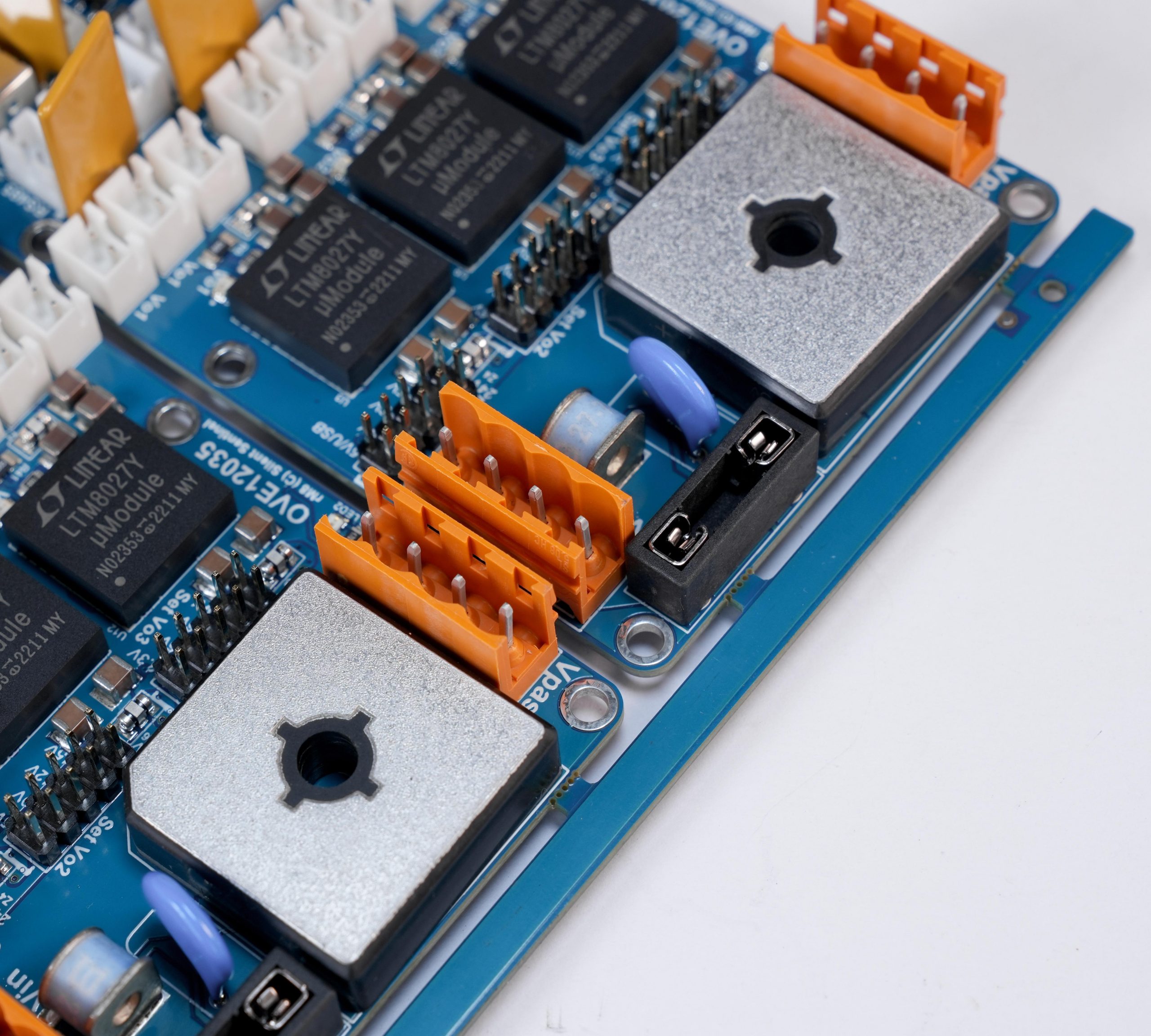
ATE PSU refers to the power supply unit (Power Supply Unit) of Automatic Test Equipment. In the field of electronic testing, ATE (automatic test equipment) is mainly used for integrated systems of power supply electrical performance testing. The system consists of test equipment hardware and test system software, and is designed to provide efficient and accurate automatic testing functions.
The key to ATE test system integration is to combine test software, test hardware (such as oscilloscopes, digital multimeters, vector networks, etc.) with communication technology to meet the testing needs of products. With the increasing complexity of electronic products, the role of ATE test system integration has become indispensable.
As part of the ATE system, the power supply unit (PSU) is responsible for providing a stable power supply for the entire test system to ensure the accuracy and reliability of the test.
Therefore, ATE PSU is one of the very important components in the ATE system, and its performance directly affects the overall efficiency and accuracy of the ATE test system.
What are the advantages of ATE?
ATE test system has the following significant advantages:
- High efficiency and time saving: ATE test system can automatically complete the test without manual intervention, which greatly saves test time and improves production efficiency.
- Easy to operate: The operation is simple and easy to understand, easy to get started, which reduces the skill requirements for operators and reduces training costs.
- Safe and reliable: The danger of manual operation can be avoided during the test process to ensure the life safety of employees.
- Improve test efficiency: Automatically execute the test program, greatly shorten the test cycle, reduce manual intervention, and thus significantly improve test efficiency.
- Flexibility and scalability: It can be flexibly configured and adjusted according to different test requirements, and supports customized configuration of various test modules and sensors.
- Reduced labor costs: Reduced dependence on labor, reduced labor costs, and improved labor efficiency.
- Strong anti-interference ability: The internal mechanical properties are good, and various external interferences can be eliminated to ensure the stability and accuracy of the test results.
In summary, the ATE test system is of great significance in improving production efficiency, reducing costs, ensuring employee safety, and optimizing quality management. It is widely used in product testing in semiconductors, electronics, automobiles and other fields.
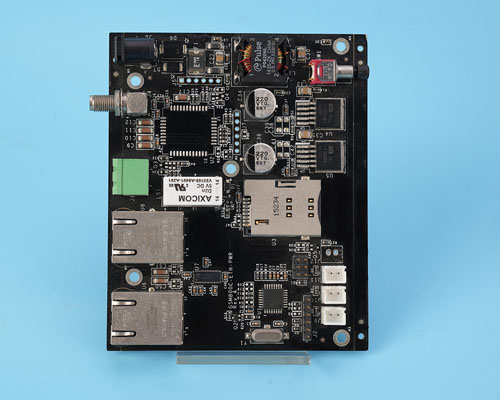
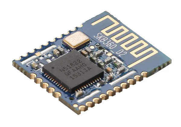
What is ate in PCB?
ATE in PCB refers to automatic test equipment (Automatic Test Equipment). ATE is a computer-controlled device used to test devices, circuit boards, and subsystems.
It replaces manual labor through computer programming and automatically completes the test sequence. In the semiconductor industry, ATE specifically refers to an automatic tester for integrated circuits (ICs), whose functions include detecting the integrity of integrated circuit functions and ensuring the quality of integrated circuit manufacturing.
In a broader context, ATE equipment can perform chip parameter testing, functional testing, performance testing, fault detection, reliability testing, etc., and plays a vital role in the semiconductor manufacturing process.
What is the difference between automatic and manual testing?
In PCB testing, there are the following differences between automatic testing and manual testing:
- 1. Automatic testing relies on equipment and software, and is programmed; manual testing is manually operated and more flexible.
- 2. Automatic testing is high-speed and efficient, and can run continuously; manual testing is slow, easy to fatigue and low efficiency.
- 3. Automatic testing has high accuracy and good consistency; manual testing is easily affected by human factors and has poor consistency.
- 4. Automatic testing equipment has high investment but low operating cost; manual testing equipment has low cost but high labor cost.
- 5. Automated testing is suitable for large-scale production and complex circuit boards; manual testing is suitable for small-batch production and fault diagnosis.
What is the purpose of automated testing?
The purpose of automated testing in PCB is to ensure that each circuit board can meet the high performance required in complex electrical applications, and to improve product quality and performance by detecting and repairing defects.
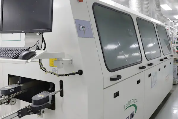
Automated testing, especially in the PCB (printed circuit board) production process, plays a vital role. This test uses machine scanners with light imaging to visually inspect the finished circuit board and evaluate the process quality by using technologies such as automated optical inspection (AOI).
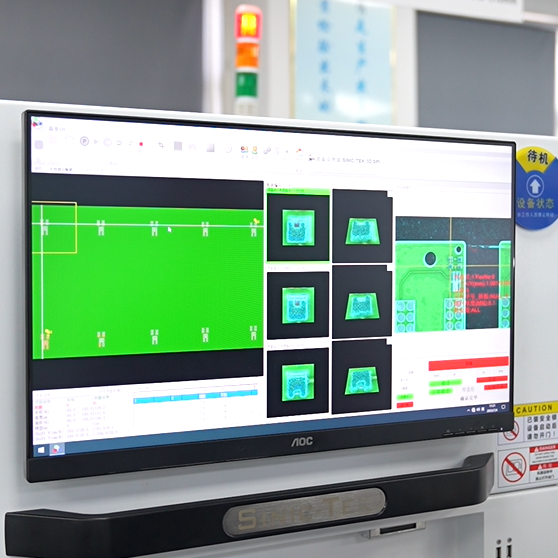
The importance of automated testing lies in its ability to detect and repair defects at multiple stages of production, including bare board inspection, solder paste inspection, pre-reflow and post-reflow. Improve production speed and productivity to ensure that tasks are completed on time.
Conclusion:
Automated test equipment (ATE) plays a key role in PCBA testing. It can improve test efficiency, accuracy and product quality, reduce test costs, and provide strong support for electronic manufacturing companies. With the continuous development of electronic technology, ATE will also continue to upgrade and improve to adapt to the increasingly complex PCBA testing needs.