Looking for LED PCB reverse engineering? Explore its processes, compliance, and manufacturer criteria to optimize LED system reliability, performance, and cost.
EBest Circuit (Best Technology) stands out as a leading LED PCB reverse engineering manufacturer, providing OEM-tailored solutions for custom LED designs. Leveraging expertise in high-resolution layer scanning and EDA tools like Altium, our team reconstructs complex circuits with meticulous precision. We specialize in modernizing obsolete PCBs by integrating contemporary components, significantly improving thermal efficiency and overall reliability. OEM clients gain comprehensive customization options—ranging from driver IC upgrades to advanced conformal coating enhancements. Certified to ISO 9001:2015 and UL standards, EBest Circuit (Best Technology) guarantees quality through stringent testing protocols and DFM optimization. Collaborating with premier LED suppliers, we deliver scalable solutions supported by lifetime warranties. For OEMs pursuing innovative LED PCB retrofits or cutting-edge designs, EBest Circuit (Best Technology) merges technical excellence with agile, client-centric service. Contact us today sales@bestpcbs.com if you have any request for LED PCB reverse engineering.
What Is LED PCB Reverse Engineering?
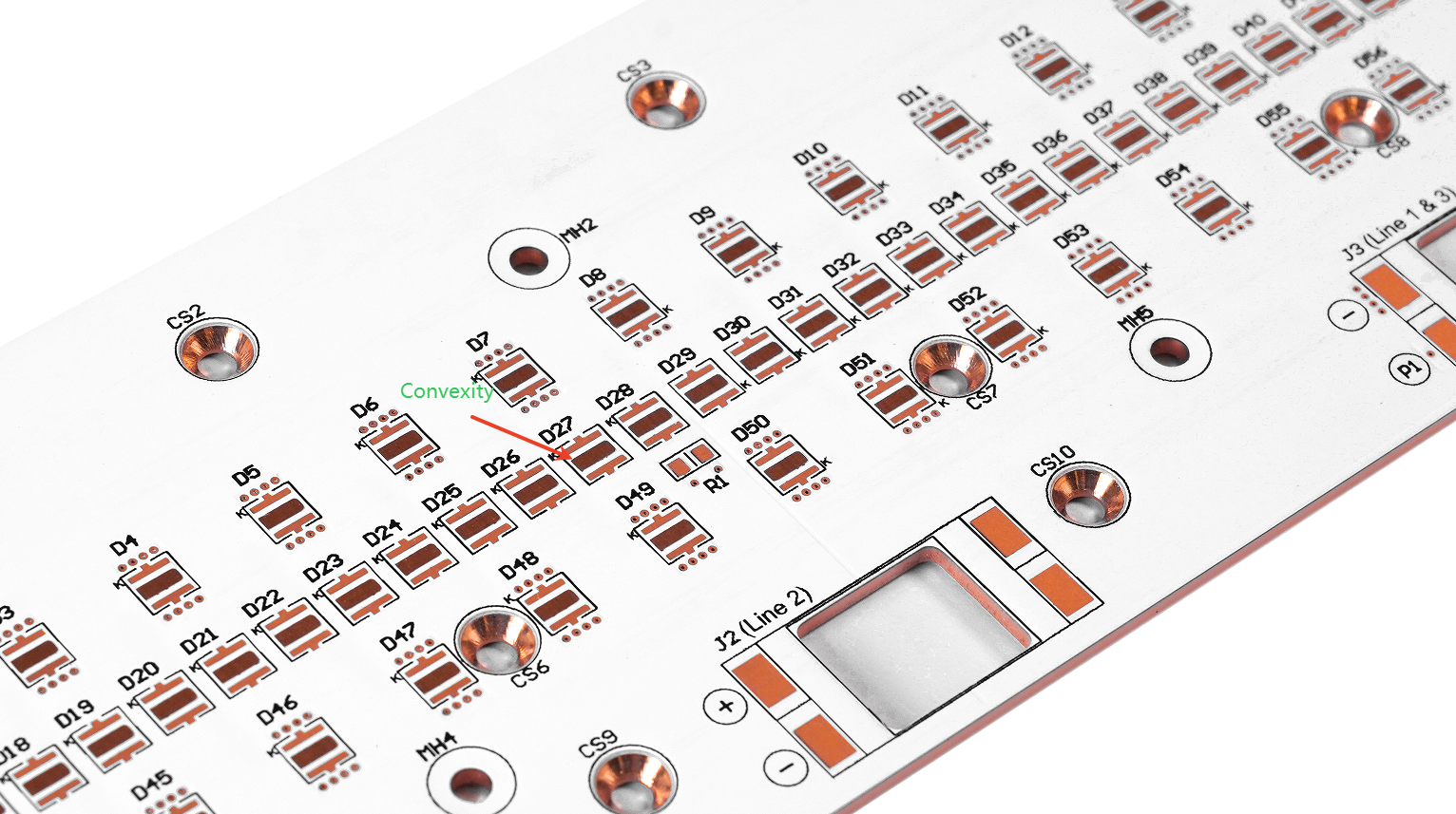
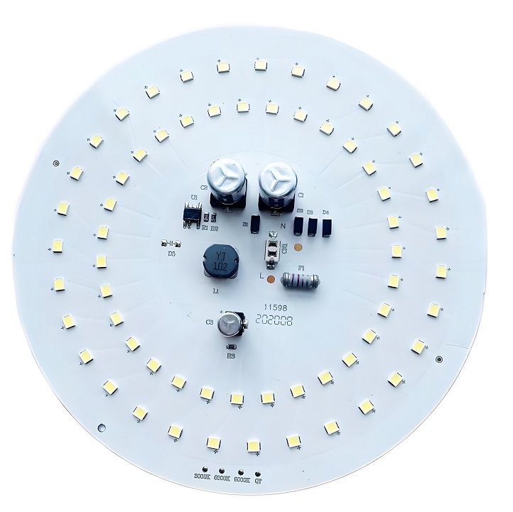
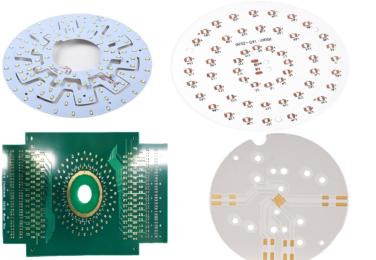
LED PCB reverse engineering is the systematic analysis of an existing LED circuit board to decode its design, component layout, and functional behavior. By disassembling the board, tracing electrical pathways, and testing performance, engineers reconstruct its schematic or identify flaws. This process enables replication, upgrades, or repairs without access to original design files, making it essential for legacy systems, cost optimization, or adapting outdated technology.
What Are Types of LED PCB Reverse Engineering?
Types of LED PCB Reverse Engineering:
- Functional Reverse Engineering-Reconstructing schematics to replicate or debug existing LED PCB functionality, such as driver circuits or dimming controls.
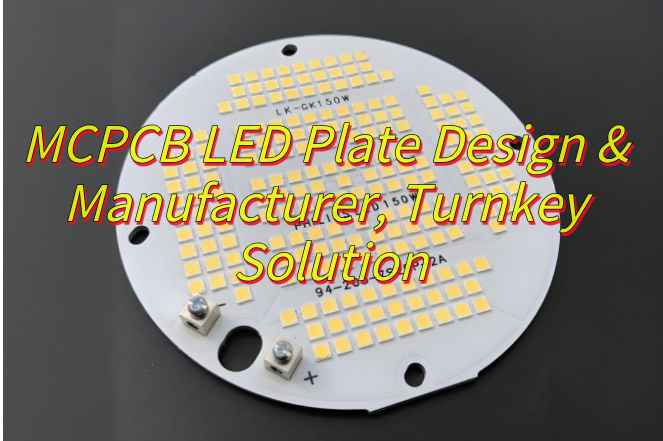
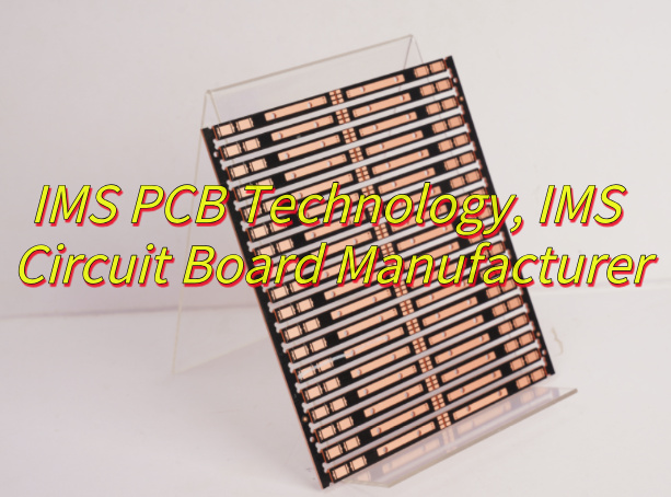
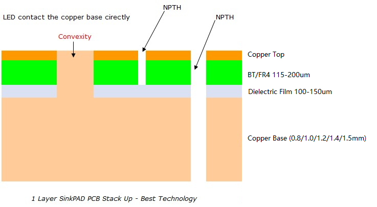
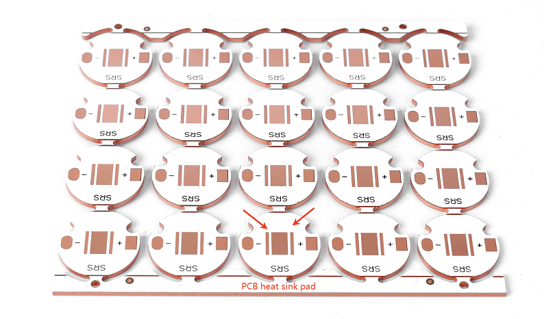
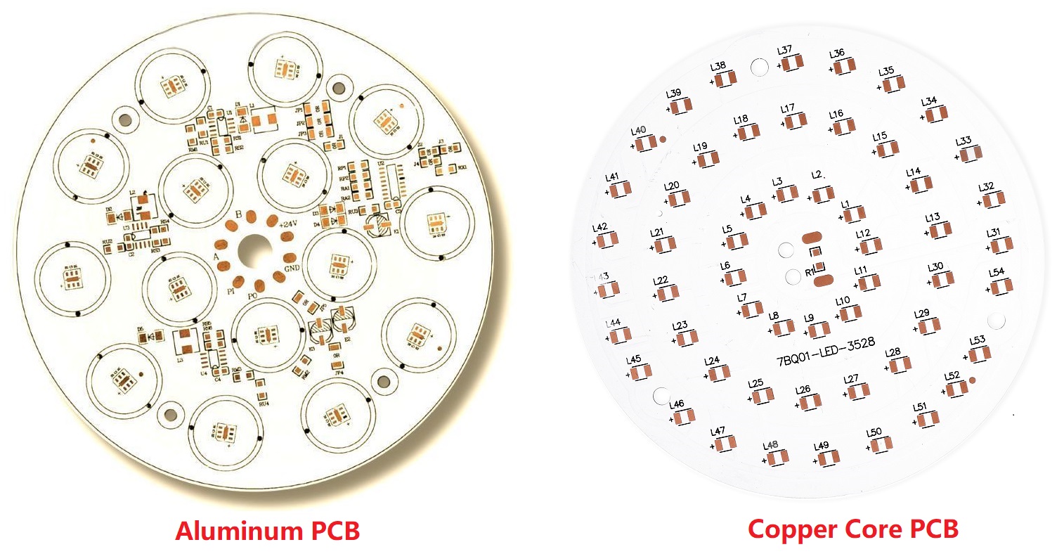
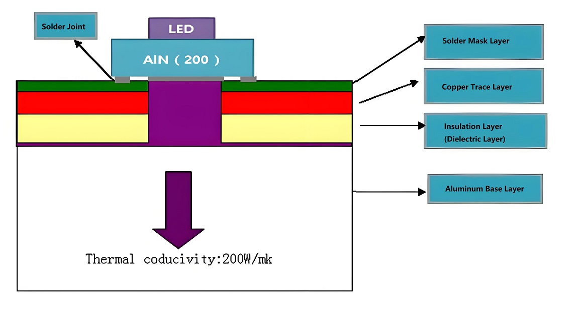
- Material Based Reverse Engineering-Analyzing substrates like aluminum-core PCBs (for heat dissipation) or FR4 boards to optimize thermal and electrical performance.
- Application Specific Reverse Engineering-Adapting designs for niche uses (e.g., automotive LED lighting, medical-grade panels, or industrial signage) to meet performance requirements.
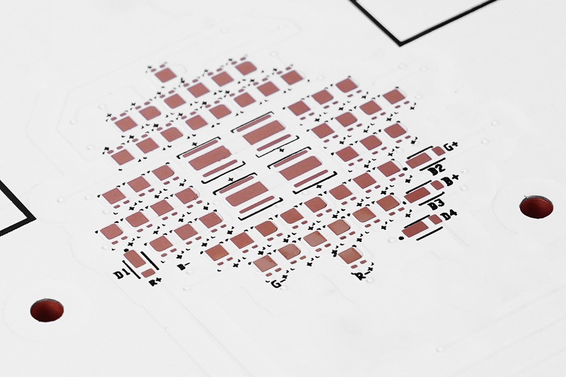
- Multi-Layer PCB Reverse Engineering-Decoding complex layouts in multi-layer LED PCBs, often used in high-density applications like display backlighting.
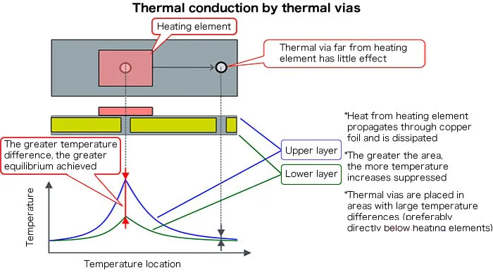
- Thermal Management-Focused Reverse Engineering-Identifying heat sink integration, trace routing, or material choices to address overheating in high-power LED systems.
- Legacy System Adaptation-Modernizing outdated LED PCBs by replacing obsolete components or upgrading firmware while retaining original form factors.
- Automated Reverse Engineering-Using software tools to accelerate trace mapping and component identification in large-scale LED PCB projects.
- Compliance-Driven Reverse Engineering-Ensuring designs meet industry standards (e.g., IEC, SIL) for safety and reliability in commercial or industrial LED applications.

What Are Advantages of LED PCB Reverse Engineering?
Advantages of LED PCB Reverse Engineering:
- Replicates legacy designs: Recreates schematics and Gerber files for obsolete LED boards when original documentation is lost or outdated.
- Identifies design flaws: Diagnoses thermal stress points or electrical inefficiencies through layer-by-layer circuit analysis.
- Accelerates prototyping: Generates BOM lists and layout diagrams to fast-track replacements or upgrades without restarting R&D.
- Reduces production costs: Avoids licensing fees for proprietary LED driver circuits by reverse-engineering compatible alternatives.
- Enables component-level repairs: Maps failed ICs or resistors in LED arrays to simplify troubleshooting and part replacement.
- Optimizes thermal performance: Analyzes aluminum-core PCB designs to improve heat dissipation in high-power LED applications.
- Supports compliance updates: Modifies outdated boards to meet modern safety standards (e.g., IEC 62471 for photobiological safety).

What Are the Steps for Reverse Engineering on LED PCBs?
1. Deconstruction & Damage Assessment
- Disassemble LED PCB layers, documenting component types (e.g., SMD LEDs, capacitors) and failure modes (e.g., delamination, burnt traces).
- Use a thermal imaging camera (e.g., FLIR TG165) to identify hotspots or damaged areas.
2. High-Resolution Imaging & Data Extraction
- Scan PCB layers with a multi-layer imaging system to capture traces, vias, and solder joints.
- Extract 3D models of components using CT scanning tools for precise re-design.
3. Schematic & Layout Reconstruction
- Reverse-engineer schematics in Altium Designer or KiCad, prioritizing LED driver circuits and power distribution.
- Rebuild PCB layouts layer by layer, referencing scans to replicate impedance-controlled traces or thermal pads.
4. Material & Component Analysis
- Test substrate materials (e.g., FR-4 vs. ceramic) via thermal cycling (-40°C to 125°C) or dielectric testing.
- Cross-reference components with datasheets to identify obsolete parts needing replacement.
- Redesign for Reliability
- Optimize trace widths, copper pours, and thermal vias using ANSYS Ice-pak simulations.
- Replace fragile components (e.g., electrolytic capacitors) with solid-state alternatives for harsh environments.
5. Repair & Rework Execution
- Use laser-assisted soldering stations to replace damaged LEDs or drivers.
- Apply conformal coatings to protect against moisture or vibration.
6. Functional Validation & Testing
- Test optical performance with integrating spheres to measure lumen output.
- Validate electrical parameters (e.g., forward voltage, current draw) using multimeters.
7. Documentation & Scalable Production
- Generate Gerber files, BOMs, and assembly instructions for contract manufacturers like EBest Circuit (Best Technology).
- Implement DFMA (Design for Manufacturing/Assembly) principles to reduce production costs by 20-30%.

What Is the Best Example of LED PCB Reverse Engineering?
Case Study: Retrofitting an Obsolete LED Streetlight PCB
Initial Assessment & Deconstruction
- Challenge: A 10-year-old LED streetlight PCB with failed capacitors and corroded traces.
- Action: Disassembled layers using a vacuum de-soldering station to preserve fragile SMD LEDs. Documented component obsolescence (e.g., discontinued LED drivers).
3D Scanning & Data Extraction
- Challenge: Capturing complex thermal pad geometries and buried vias.
- Action: Scanned PCB layers with a high-resolution CT scanner to generate 3D models. Extracted trace impedance data using TDR (Time Domain Reflectometry) tools.
Redesign for Modern Components
- Challenge: Replacing obsolete drivers with newer ICs.
- Action: Redesigned power circuits in Altium Designer to accommodate smaller form-factor components; And added over-temperature protection circuits using thermistors and MOSFETs.
Material Upgrades & Thermal Optimization
- Challenge: Original aluminum-core PCB suffered from thermal expansion stress.
- Action: Switched to a copper-clad FR-4 substrate with embedded copper coins for heat sinking; And simulated thermal performance in ANSYS Ice-pak, reducing junction temperatures by 15°C.
Repair & Structural Reinforcement
- Challenge: Delaminated prepreg layers near LED clusters.
- Action: Reinforced high-stress areas with epoxy underfill; Replaced electrolytic capacitors with solid polymer capacitors.
Firmware Reverse-Engineering & Updates
- Challenge: Proprietary LED dimming firmware was encrypted.
- Action: Used a logic analyzer to capture I2C communication protocols; Rewrote firmware in C++ to add IoT connectivity.
Validation & Field Testing
- Challenge: Ensuring compliance with LM-80/TM-21 standards.
- Action: Tested lumen maintenance over 6,000 hours using a goniophotometer (e.g., LED6000); Validated surge protection (6 kV/1.2/50 μs) using a Hi-pot tester.
Scalability & Cost Reduction
Outcome:
- Reduced BOM cost by 22% through component standardization.
- Improved energy efficiency from 110 lm/W to 135 lm/W.
- Extended product lifespan from 50,000 hours to 80,000 hours (MTBF).
- Final Result: A retrofitted LED PCB design adopted by 12 municipal projects, with 35% lower maintenance costs and 20% higher light output uniformity.
How to Choose a Reliable LED PCB Reverse Engineering Manufacturer?
Here’s how to choose a reliable LED PCB reverse engineering manufacturer:
Verify Technical Capabilities
- Scanning Precision: Ensure they use high-resolution systems (e.g., 12μm layer scanning) and CT scanning for buried vias.
- EDA Tool Mastery: Look for expertise in Altium, KiCad, or Siemens NX for redesigning complex LED driver circuits.
Assess Redesign & Repair Expertise
- Component Replacement: Confirm experience with obsolete part substitution (e.g., replacing discontinued LED arrays).
- Thermal Optimization: Check case studies showing improved heat dissipation via via redistribution or copper pours.
Evaluate Service Breadth
- Full-Cycle Support: Choose manufacturers offering end-to-end services—from deconstruction to prototype testing.
- Scalability: Ensure they handle both small repairs and mass production redesigns (e.g., 10-unit vs. 10,000-unit projects).
Audit Quality Certifications
- ISO Standards: Prioritize ISO 9001:2015 and ISO 13485 (for medical LED devices) compliance.
- UL/CE Testing: Verify in-house facilities for safety certifications to avoid third-party delays.
Review Case Studies & Portfolio
- Complex Projects: Seek examples of redesigns involving SMT LEDs, flexible PCBs, or water-resistant coatings.
- Repair Success: Look for documented repairs of delamination, trace corrosion, or driver IC failures.
Communication & Documentation
- Transparency: Ensure clear milestones, weekly progress reports, and access to design files (Gerber, BOM).
- Post-Project Support: Confirm availability of DFM feedback or warranty-covered adjustments.
Cost & Value Analysis
- Avoid Hidden Fees: Clarify costs for scanning, redesign, prototyping, and certification.
- Long-Term Savings: Prioritize manufacturers who optimize designs to reduce material waste or assembly errors.
How Do Manufacturers Ensure Design Compliance in LED PCB Repair and Redesign?
LED PCB manufacturers must prioritize design compliance to meet safety, performance, and regulatory standards. Here’s how industry leaders achieve this:
Certification & Standards Adherence
- Maintain ISO 9001:2015 and IPC-A-610 certifications to standardize quality control.
- Comply with regional regulations (e.g., UL/CE for electrical safety, RoHS for hazardous materials).
Pre-Repair Diagnostics
- Use thermal imaging and X-ray inspection to identify failure modes (e.g., delamination, cold solder joints).
- Cross-reference original design files (Gerber, BOM) to preserve critical specifications.
Material & Component Validation
- Replace obsolete parts with equivalents meeting original form, fit, and function (FFF) criteria.
- Test substitute materials (e.g., FR-4 vs. ceramic substrates) under extreme conditions (-40°C to 125°C).
Redesign for Reliability
- Optimize trace widths, via density, and thermal pads using ANSYS simulations.
- Incorporate surge protection (e.g., TVS diodes) and conformal coatings for harsh environments.
Post-Redesign Verification
- Validate electrical parameters (e.g., impedance, voltage drop) with multimeters.
- Conduct lumen maintenance tests (LM-80) to ensure optical performance matches OEM specs.
Documentation & Traceability
- Provide detailed test reports, including XRF material analysis and Hi-Pot safety checks.
- Offer lifetime warranties on repaired PCBs, backed by component-level failure analysis.
How Do LED PCB Reverse Engineering Manufacturers Ensure Design Accuracy?
High-Resolution Data Acquisition
- Use multi-layer PCB scanners and CT systems to capture traces, vias, and component footprints at ≤10μm precision.
EDA-Driven Design Reconstruction
- Rebuild schematics in Altium or KiCad, cross-referencing scanned images to replicate impedance-controlled traces and thermal pads.
- Validate netlists against original functionality using SPICE simulations.
Material & Component Analysis
- Test substrate dielectric properties with TDR (Time Domain Reflectometry) tools.
- Use XRF (X-Ray Fluorescence) and FTIR spectroscopy to verify solder composition and conformal coatings.
Layer-by-Layer Verification
- Compare reconstructed Gerber files to original designs using CAM350 or GC-Prevue software.
- Conduct design rule checks (DRC) to flag clearance or trace width discrepancies.
Functional Testing Protocols
- Validate electrical parameters (e.g., LED forward voltage, driver efficiency) with Keysight 34461A multimeters.
- Test thermal performance under load using FLIR thermal cameras to ensure junction temperatures match OEM specs.
Rework & Repair Precision
- Use laser-assisted soldering stations for component replacement, minimizing thermal stress on adjacent LEDs.
- Apply robotic dispensing systems for conformal coatings to ensure uniform coverage.
Documentation & Compliance
- Generate BOMs, assembly drawings, and test reports (e.g., IPC-A-610 compliance checks).
- Maintain revision history for ISO 9001:2015 audits and client traceability.
Final Accuracy Outcomes:
- Redesigned PCBs achieve <5% deviation from original lumen output and thermal resistance.
- Repaired units show 80% reduction in field failure rates post-rework.
In conclusion, that’s all about LED PCB reverse engineering processes, compliance, and manufacturer criteria to optimize LED system reliability, performance, and cost. Welcome to leave a message below this blog if you have any issues about LED PCB reverse engineering.