How to read circuit boards and schematics is a basic skill for anyone interested in electronics. Whether you’re a beginner or a technician, knowing how to read these diagrams is crucial. In this blog, we would like to share the key points and components symbols in the PCB schematics.
How to Understand a PCB Board?
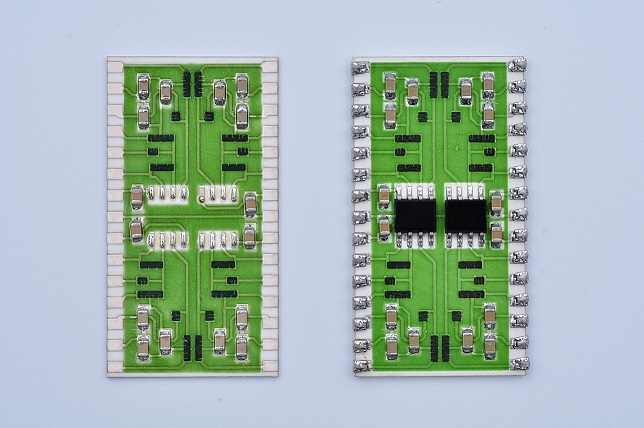
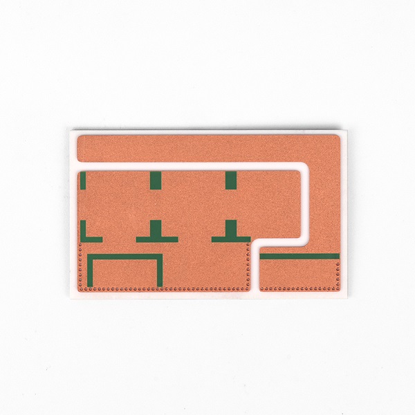
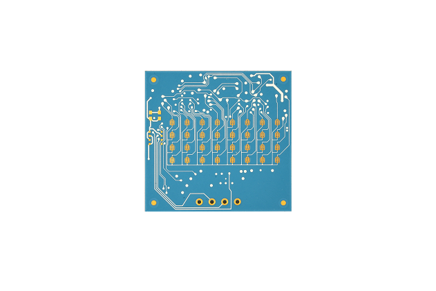
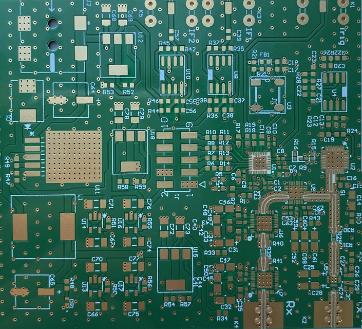
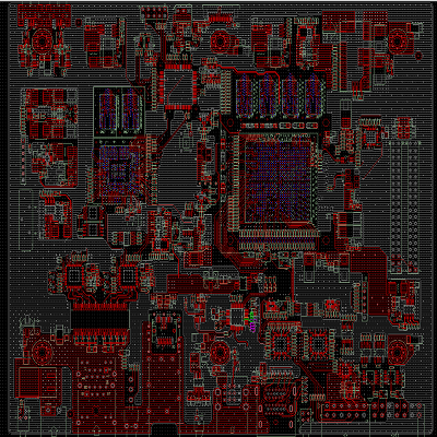
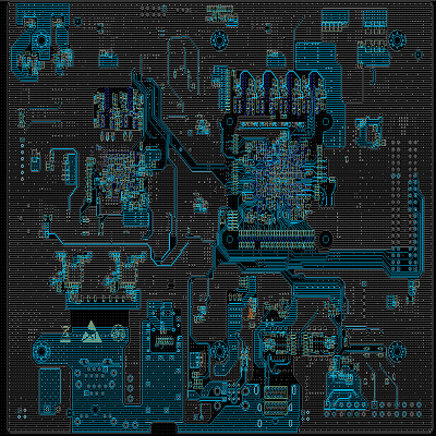
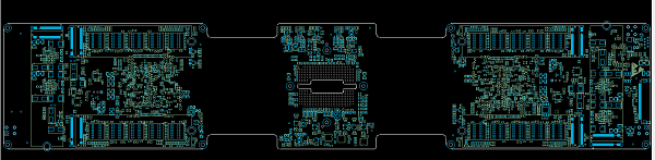
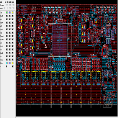
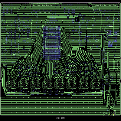
A printed circuit board is a basic of electronic components interconnected via conductive paths printed on a baseboard. We can see it everywhere. They connect and support various components using conductive tracks, pads, and other features. To understand a PCB, start by identifying its main sections: power supply, signal paths, and grounding. Look for the layout patterns, which often follow a logical flow.
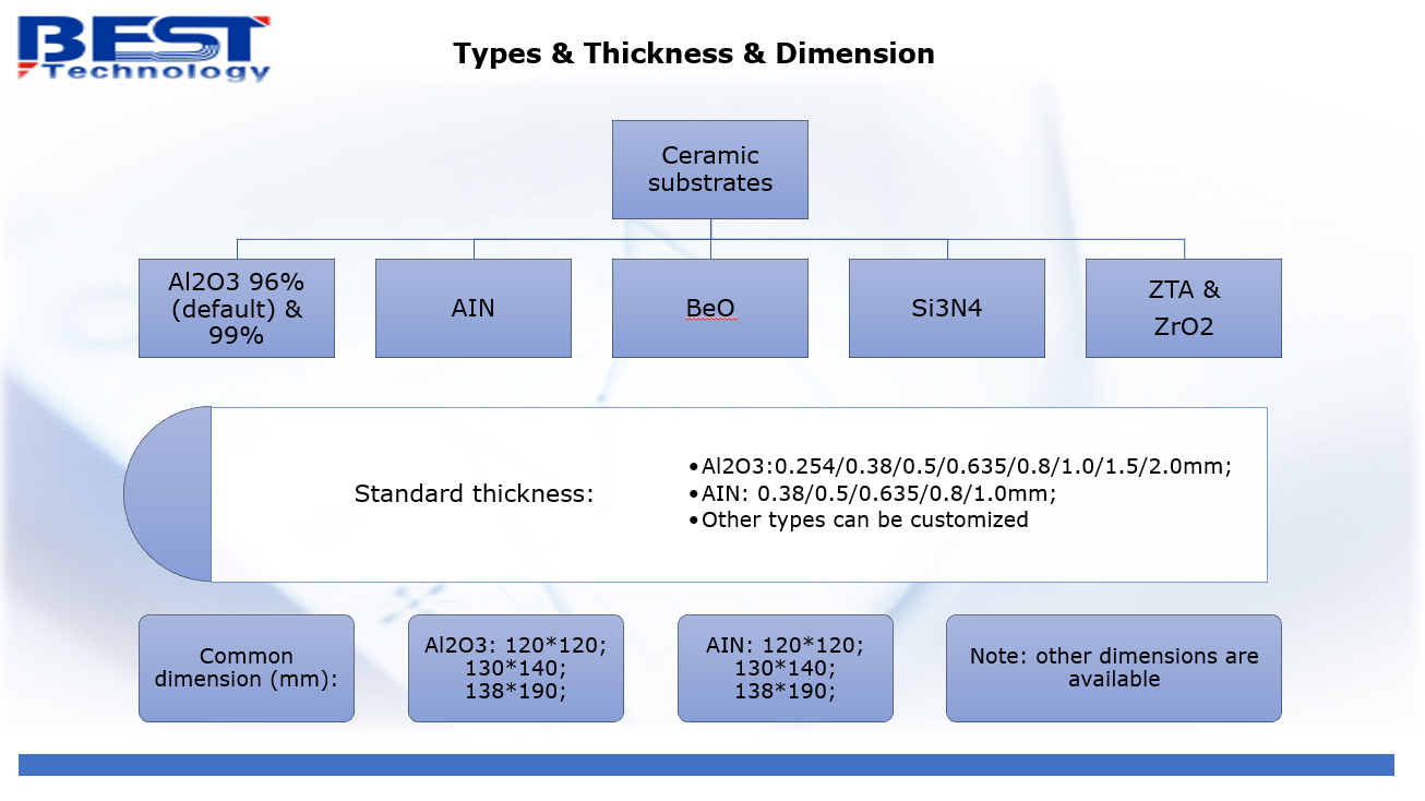
Special Types of Circuit Boards
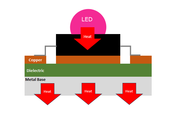
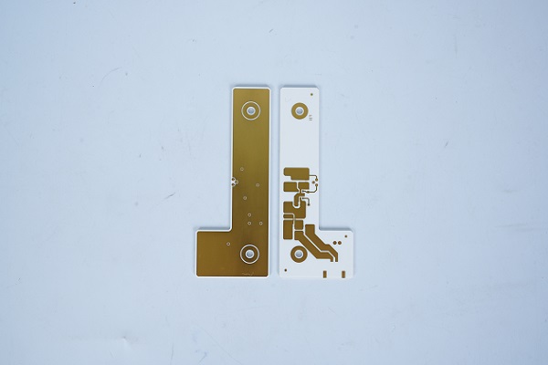
Circuit boards come in various types, each designed for specific applications and processes. Apart from the standard FR4 PCB, metal core PCB, ceramic PCB, rigid-flex PCB, there are some other special PCB uses different process. Here, we’ll explore them based on their unique manufacturing processes, including HDI, busbar, extra thin, IC substrate, high Tg, heavy copper, RF, and impedance control PCBs.
High-Density Interconnect (HDI) PCB
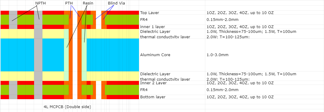
HDI PCBs are designed for compact and complex electronic devices. They feature higher wiring density per unit area compared to traditional PCBs. The process involves microvias, buried vias, and blind vias to create intricate pathways. HDI technology allows for more components on a smaller board, enhancing performance and reducing size. This type of PCB is commonly used in smartphones, tablets, and other high-tech gadgets. The HDI PCBs that EBest Circuit (Best Technology) can make is:
- 1+N+1
- 2+N+2
- 3+N+3
Busbar PCB
Busbar PCBs are specialized boards that handle high current loads efficiently. It belongs to the heavy copper PCB. They use thick copper layers to conduct electricity with minimal resistance. The busbar process involves integrating these thick copper bars within the PCB to distribute power uniformly. They are mainly used in the electric vehicles, power supplies and industrial machinery.
Extra Thin PCB
Extra thin PCBs are designed for applications where space and weight are critical constraints. These boards can be as thin as 0.2mm, allowing them to fit into slim devices like wearables and medical implants. The manufacturing process focuses on using thinner materials and precision etching techniques to achieve the desired thickness without compromising functionality.
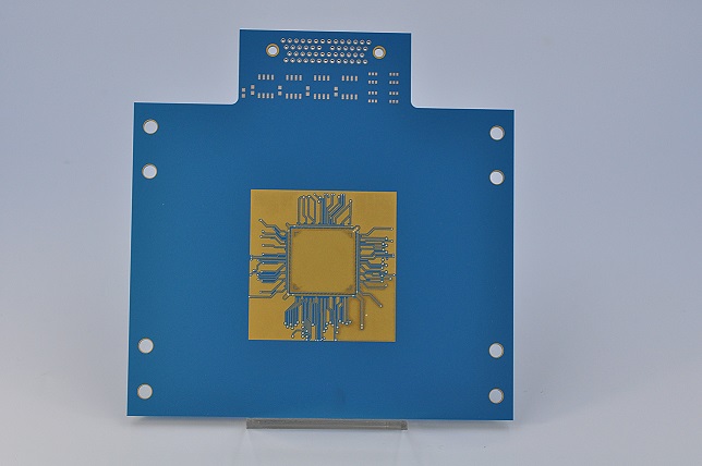
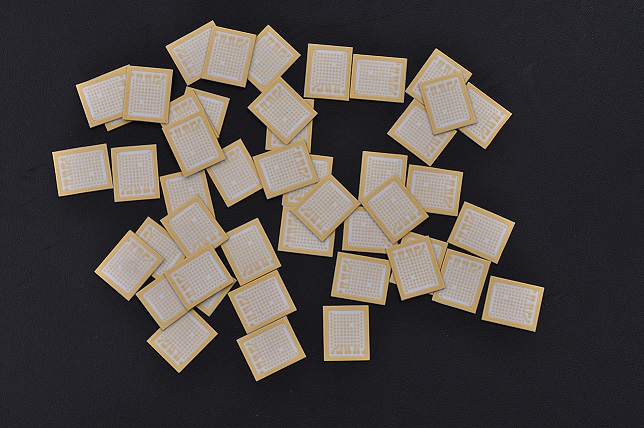
IC Substrate PCB
IC substrate PCBs act as the base for integrated circuits (IC). They provide interconnections between the IC and the PCB. These PCBs are crucial in devices like processors, memory modules, and graphic cards, where precision and reliability are paramount.
High Tg PCB
High Tg (glass transition temperature) PCBs are designed to withstand higher temperatures. The Tg value indicates the temperature at which the PCB material transitions from a rigid to a soft state. High Tg PCBs use materials that has over 170 Tg value. So, they are widely used in automotive, aerospace, and industrial applications.
Heavy Copper PCB
Heavy copper PCBs feature significantly thicker copper layers compared to standard PCBs. The process involves plating additional copper to achieve thicknesses of 3oz/ft² or more. These boards handle high currents and thermal cycles, making them ideal for power electronics, motor controllers, and high-power distribution systems.
Radio Frequency (RF) PCB
RF PCBs are designed for high-frequency applications. They use special materials like PTFE (Teflon) to minimize signal loss and interference. This kind of PCB always requires precise control over dielectric thickness and conductor widths to make sure optimal signal integrity. RF PCBs are essential in communication devices, radar systems, and microwave equipment.
What Do the Numbers on a Circuit Boards Mean?
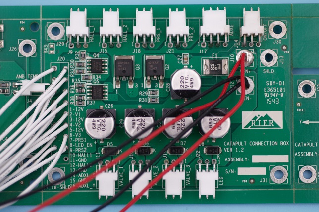
Numbers and letters on a circuit board represent component values, reference designators, and sometimes manufacturing codes. Reference designators (like R for resistors, C for capacitors) help identify each component. The numbers often indicate the order of placement or specific values (e.g., R1, R2 for the first and second resistors).
In addition, some designers prefer to design series number on the PCB board, like 202400001…202400002. For this kind of numbers, they are always aim to easy identification during the assembly or testing.
How to Read Circuit Boards?
Reading a circuit board involves several steps. First, familiarize yourself with the board’s layout and components. Identify key parts such as the microcontroller, resistors, capacitors, and connectors. Trace the pathways or traces to understand the connections. Use the reference designators to match components with their schematic symbols.
Electronic symbols follow standardized guidelines to ensure consistency. The most common standards include IEEE, IEC, and ANSI. These symbols represent various components like resistors, capacitors, diodes, and transistors.
- VCC – the positive power supply.
- GND – ground or negative power supply.
- R – resistor.
- C – capacitor.
- L – inductor.
- Q – transistor or field-effect transistor (FET).
- JP – connector or plug/socket.
- IC – integrated circuit or chip.
- + / – – input/output terminals of a signal.
- NC – no connection or an unused pin.
How Do You Read a Circuit Schematic for Beginners?
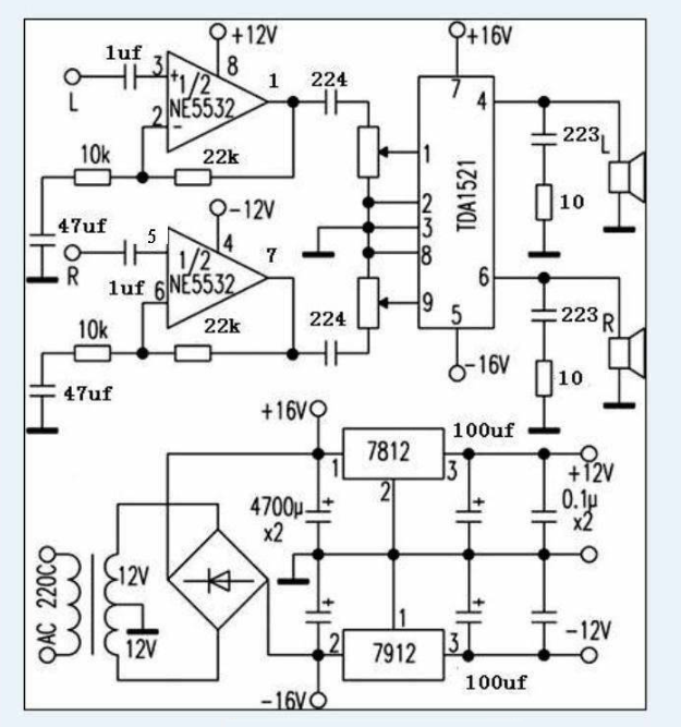
Read circuit diagram drawings can be consulted by experienced masters. Generally, the first look when reading a circuit schematic is look at the main loop. And then look at the control loop, the control loop requirements are from top to bottom or from left to right. The circuit diagram mainly consists of four parts: component symbol, connection, node and comment/note.
1. Component Symbols
These represent the actual components in the circuit. Their shapes may not resemble the actual components and can even be completely different. However, they generally indicate the characteristics of the components, and the number of pins matches the actual components.
2. Connections
These represent the wires in the actual circuit. While they appear as lines in the schematic, they are often not lines but various shapes of copper foil blocks on commonly used printed circuit boards (PCBs). For example, many connections in a radio schematic may not be line-shaped on the PCB but rather in specific shapes of copper film.
3. Nodes
These indicate the connections between multiple component pins or wires. All component pins and wires connected to a node are conductive, regardless of the number.
4. Comment/note
These are very important in a schematic. All the text in the schematic can be classified as notes. A close look at the schematics reveals annotations everywhere, used to indicate component models, names, and other information.
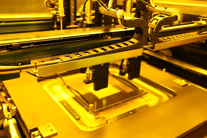
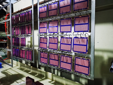
EBest Circuit (Best Technology) offer top-quality advanced PCB boards, from prototypes to mass production. Our range includes FR4 PCBs of any Tg, FPC, ceramic PCBs, aluminum PCBs, Teflon PCBs, and copper-base PCBs. Every product and service is traceable and verified with ISO, IATF, RoHS, UL, and REACH certifications. Enjoy free samples for bulk orders, complimentary functional testing, and fast delivery.