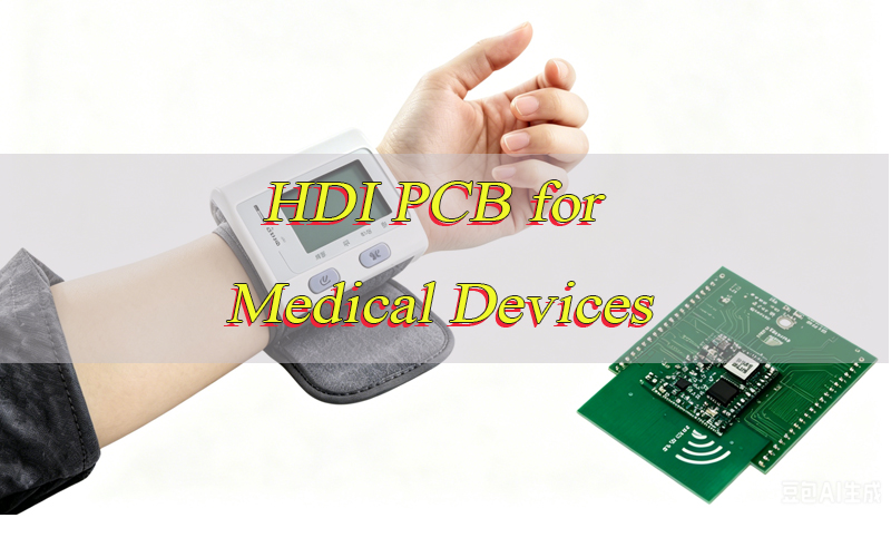
Are you searching for reliable HDI PCB for medical devices that meet strict ISO 13485 and IPC Class 3A standards? How do you ensure your medical HDI PCB is safe, fully compliant, and built for long-term reliability? In this article, we cover critical requirements, qualified materials, strict testing, DFM optimization, traceability, and how EBest delivers high-quality HDI PCB for medical devices for your healthcare projects.
Why Choose EBest Circuit as Reliable HDI PCB Fabricator for Medical Devices?
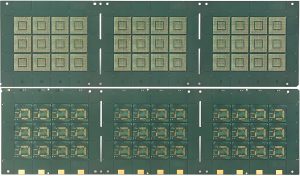
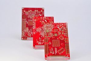
When selecting a partner for HDI PCB for medical devices, trust is earned through proven expertise, uncompromising quality, and a track record of supporting life-critical applications. EBest has established itself as a leading fabricator for medical HDI PCBs, combining 20+ years of specialized experience, rigorous certifications, and customer-centric solutions tailored to healthcare’s unique demands. Every board we produce aligns with the strictest industry standards, ensuring safety, reliability, and compliance for your medical device projects.
- 20+ Years of Medical HDI Expertise: Dedicated to medical devices HDI PCB, with 500+ successful healthcare projects delivered, from prototypes to mass production.
- Industry-Leading Production Capacity: Monthly output of 260,000 sq ft, completing 1,000+ unique boards, ensuring scalability for any project size.
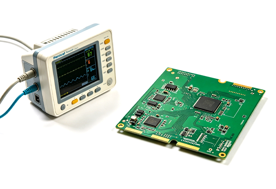
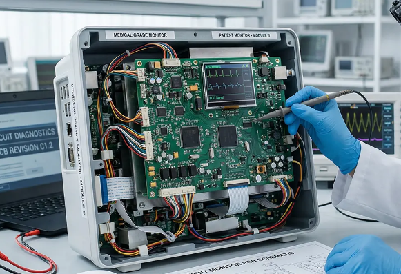
- Exceptional Reliability Rate: 99.98% product reliability for HDI PCB for medical devices, deployed in pacemakers, surgical tools, patient monitors, and diagnostic imaging systems.
- Full Regulatory Certification: ISO 13485:2016, IPC Class 3A, RoHS, UL, and REACH compliant, critical for global medical device market access.
- 24-Hour Expedited Service: Urgent HDI PCB for medical devices orders shipped within 24 hours without compromising quality, supporting time-sensitive healthcare innovations.
- Cross-Industry Proven Performance: Extensive experience delivering high-reliability PCBs for medical, aerospace, and industrial electronics, validating our technical capabilities.
What Technical Requirements Must Medical-Grade HDI PCBs Meet?
Medical-grade HDI PCB for medical devices demand far stricter technical specifications than consumer electronics, as they directly impact patient safety and device longevity. These requirements ensure electrical stability, mechanical durability, biocompatibility, and resistance to harsh medical environments like sterilization and continuous operation. Below is a detailed breakdown of non-negotiable technical standards for medical HDI PCBs, aligned with IPC Class 3A and ISO 13485.
| Parameter | Requirement for HDI PCB for Medical Devices |
|---|---|
| Core Compliance | ISO 13485, IPC-6012 Class 3A, IPC-A-610 Class 3, IEC 60601-1 |
| Minimum Line Width/Spacing | 2/2 mil (inner layer), 2.5/2.5 mil (outer layer) |
| Microvia Diameter | ≥0.1mm (laser-drilled, stacked/staggered configurations) |
| Dielectric Thickness | ≥0.1mm (±10% tolerance for consistent signal integrity) |
| Glass Transition Temperature (Tg) | ≥170°C (high thermal stability for sterilization and cycling) |
| Copper Plating Thickness | ≥18μm (uniform, zero voids in vias; ≥25μm internal, ≥50μm external for high-current) |
| Biocompatibility | USP Class VI, ISO 10993 (non-cytotoxic, no harmful leachables) |
| Sterilization Resistance | Autoclave (121°C), EtO, gamma irradiation (25kGy) compatible |
| Impedance Control | ±5% tolerance for high-speed signals (critical for imaging/monitoring) |
| Df (Dissipation Factor) | ≤0.004 (low signal loss for high-frequency medical electronics) |
How Do We Ensure Compliance with ISO 13485 and IPC Class 3A for Medical HDI PCBs?
Compliance with ISO 13485 (medical quality management) and IPC Class 3A (highest reliability for life-critical devices) is non-negotiable for medical devices HDI PCB. These standards mitigate risk, ensure consistent quality, and streamline regulatory approvals. At EBest, we embed these requirements into every production stage, from design to delivery, with zero tolerance for deviations.
- ISO 13485-Certified QMS: Dedicated quality management system for HDI PCB for medical devices, integrating ISO 14971 risk management (FMEA) at every stage.
- IPC Class 3A Process Controls: Strict tolerances for microvias, annular rings (≥1mil internal/≥2mil external), and copper uniformity; zero breakout tolerance.
- 100% In-Process Inspections: Critical stage checks (lamination, laser drilling, plating) to catch defects early and maintain Class 3A workmanship.
- Qualified Material Sourcing: All raw materials for HDI PCB for medical devices sourced from ISO-audited suppliers, with batch-level traceability.
- Quarterly Internal Audits: Rigorous reviews of processes, documentation, and quality metrics to align with latest ISO 13485 and IPC updates.
- Annual Third-Party Certification: Independent audits to validate compliance, ensuring global regulatory recognition for your medical device HDI PCB.
- Full Compliance Documentation: Device Master Records (DMR) and Device History Records (DHR) for regulatory submissions (FDA 21 CFR Part 820, EU MDR).
What Materials and Surface Finishes Does We Recommend for Medical HDI PCBs?
Material and surface finish selection directly determines the reliability, biocompatibility, and lifespan of HDI PCB for medical devices. Poor choices risk corrosion, signal degradation, or cytotoxicity, critical failures in medical applications. EBest exclusively recommends medical-grade options that meet ISO 10993 and USP Class VI standards, balancing performance, durability, and safety.
Top Recommended Substrate Materials
- High-Reliability FR-4 (Tg ≥170°C): Industry standard for external HDI PCB for medical devices; low Df (≤0.004), stable Dk, and excellent dimensional stability to resist warping.
- Polyimide (PI): Flexible, heat-resistant (-40°C to +200°C); ideal for wearable and implantable HDI PCB for medical devices with direct tissue contact.
- LCP (Liquid Crystal Polymer): Ultra-low loss, biocompatible; perfect for high-frequency diagnostic equipment (MRI, ultrasound) requiring minimal signal interference.
- BT Resin: Superior thermal stability for stacked microvias in high-density HDI PCB for medical devices; low moisture absorption prevents delamination.
Premium Recommended Surface Finishes
- ENIG (Electroless Nickel Immersion Gold): Industry standard for HDI PCB for medical devices; flat surface (coplanarity <0.01mm), corrosion-resistant, and supports fine-pitch BGA assembly.
- ENEPIG: Enhanced wire bonding capability for hybrid medical assemblies; ideal for long-term reliability in implantable HDI PCB for medical devices.
- OSP (Organic Solderability Preservative): Cost-effective, lead-free, and biocompatible; suitable for low-risk external HDI PCB for medical devices.
- Immersion Silver: Low contact resistance; perfect for high-speed signal paths in diagnostic HDI PCB for medical devices (e.g., ECG monitors).
- Finishes to Avoid: Immersion tin/HASL (tin whisker risk causing short circuits) and lead-based finishes (prohibited by RoHS and medical regulations).
What Rigorous Testing Protocols Does We Implement for Medical HDI PCBs?
HDI PCB for medical devices must undergo comprehensive, multi-level testing to ensure zero defects and reliable performance under harsh medical conditions. EBest’s testing protocols exceed industry minimums, validating electrical, mechanical, and biocompatibility performance for life-critical applications. Every board is tested to confirm compliance with ISO 13485 and IPC Class 3A.
- 100% Electrical Testing: Continuity, isolation, and impedance control checks (±5% tolerance) for every HDI PCB for medical devices.
- 3D AOI Inspection: Detects surface defects, soldering issues, and dimensional errors in microvias and fine traces.
- X-Ray Inspection: Identifies hidden microvia voids, layer misalignment, and BGA joint quality, critical for HDI reliability.
- Thermal Cycling Test: -40°C to +125°C for 1,000 cycles to validate microvia and laminate stability during sterilization/operation.
- Biocompatibility Testing: USP Class VI cytotoxicity and ISO 10993 irritation tests for HDI PCB for medical devices with direct patient contact.
- Sterilization Resistance Test: Autoclave (121°C), EtO, and gamma irradiation exposure to confirm performance post-sterilization.
- Cross-Section Analysis: Verifies copper plating uniformity, resin fill, and microvia integrity for stacked HDI structures.
- Environmental Exposure Testing: Humidity (85% RH, 85°C) and aging tests to simulate 10+ years of clinical use.
How Can We Support Your HDI PCB Design for Manufacturability (DFM) in Medical Projects?
Design for Manufacturability (DFM) is critical for medical HDI PCB to avoid production delays, reduce costs, and maintain regulatory compliance. Medical HDI designs are complex, with microvias, fine traces, and strict tolerance requirements, making proactive DFM support essential. EBest’s engineering team provides end-to-end DFM guidance tailored to medical project needs, ensuring your design is manufacturable, reliable, and compliant.
- Free Early DFM Review: Comprehensive analysis of HDI PCB for medical devices schematics/layouts to identify risks (microvia spacing, line width, annular ring size) pre-production.
- HDI Structure Optimization: Custom 2+N+2/3+N+3 stackup design for HDI PCB for medical devices, balancing density, reliability, and signal integrity.
- Material & Stackup Guidance: Medical-grade substrate/prepreg recommendations for HDI PCB for medical devices, ensuring CTE matching and thermal stability.
- Regulatory-Aligned DFM Adjustments: Layout modifications to meet IPC Class 3A and ISO 13485 requirements (e.g., minimum annular ring size, creepage/clearance).
- Impedance Control Guidance: Expert recommendations for high-speed HDI PCB for medical devices (imaging/monitoring) to minimize crosstalk.
- Fast Prototype Validation: 2–3 day prototype runs for HDI PCB for medical devices to test DFM changes before mass production.
- DFM Documentation: Detailed records of all design adjustments for traceability and regulatory submissions.
How Does We Ensure Full Traceability and Regulatory Documentation for Medical HDI PCBs?
Medical device regulations (ISO 13485, FDA, EU MDR) require complete traceability and comprehensive documentation for HDI PCB for medical devices. These records are critical for audits, regulatory approvals, and post-market surveillance. EBest implements a full-lot traceability system and maintains detailed, English-language documentation for every medical HDI PCB produced.
- Unique Lot ID Tracking: Every HDI PCB for medical devices assigned a unique ID, linking raw material lots, production parameters, equipment, and operator data.
- Material Traceability Records: Certificates of Analysis (CoA) for all substrates, copper, surface finishes, and solder masks used in HDI PCB for medical devices.
- Detailed Process Logs: Real-time records of lamination, laser drilling, plating, AOI/X-ray inspection, and testing for each HDI PCB for medical devices batch.
- Full Test Reports: Comprehensive documentation of electrical, thermal, biocompatibility, and sterilization tests for HDI PCB for medical devices.
- Long-Term Record Retention: All HDI PCB for medical devices records stored for 7+ years (20+ years for implantable devices) per regulatory requirements.
- Batch Genealogy Access: Full traceability available for every HDI PCB for medical devices unit, enabling complete genealogy tracking for audits.
- Regulatory-Ready Documentation: Device Master Records (DMR) and Device History Records (DHR) formatted for global regulatory bodies (FDA, EU MDR).
How to Choose Reliable HDI PCB for Medical Devices for Your Healthcare Projects?
Selecting a reliable supplier for HDI PCB for medical devices is one of the most critical decisions for your healthcare project. Poor quality can risk patient safety, regulatory delays, and project failure. The right partner combines medical expertise, strict compliance, advanced testing, and proven experience. Below is a step-by-step guide to selecting a trusted supplier for your HDI PCB for medical devices.
- Verify Medical-Specific Certifications: Confirm ISO 13485:2016, IPC Class 3A, USP Class VI, and RoHS certifications for HDI PCB for medical devices production.
- Assess HDI Specialization: Evaluate experience with microvias (≥0.1mm), fine-pitch components, and high-density stackups (2+N+2/3+N+3) for HDI PCB for medical devices.
- Review In-House Testing Capabilities: Ensure the supplier offers 100% electrical, 3D AOI/X-ray, thermal cycling, and biocompatibility testing for HDI PCB for medical devices.
- Confirm Full Traceability Systems: Verify unique lot ID tracking and complete material/process traceability for every HDI PCB for medical devices.
- Evaluate Production Scalability: Check ability to scale from prototypes (2–3 days) to mass production (5–10 days) for HDI PCB for medical devices without quality compromise.
- Check Medical Project References: Request case studies or references for HDI PCB for medical devices projects (implantable devices, diagnostic imaging, wearables).
- Assess Engineering Support: Ensure dedicated DFM guidance, material selection expertise, and regulatory support for HDI PCB for medical devices.
- Validate Material Sourcing: Confirm raw materials for HDI PCB for medical devices are sourced from ISO-qualified, medical-grade suppliers.
FAQ About HDI PCB for Medical Devices
Q1: What is the difference between IPC Class 3 and Class 3A for medical applications?
A1: IPC Class 3 covers general high-reliability electronics. Class 3A is a stricter standard for life-sustaining and implantable medical devices. It enforces tighter tolerances for microvias, annular rings and copper plating, ensuring higher safety margins for patients.
Q2: Can medical HDI PCBs be used in implantable devices?
A2: Yes. When built with biocompatible materials like polyimide or LCP and certified USP Class VI/ISO 10993, medical HDI PCBs can safely support implantable applications. They must also resist common sterilization methods.
Q3: What surface finishes should be avoided for medical PCBs?
A3: Immersion tin and HASL are not recommended. Tin whiskers can cause short circuits in fine-pitch designs. Lead-based finishes are also prohibited by RoHS and medical safety regulations.
Q4: How long does production take for custom medical HDI boards at EBest?
A4: Standard lead time is 5–10 days. Expedited 24-hour service is available for urgent projects. Prototypes can be ready in 2–3 days with full DFM and compliance documentation included.
Q5: What global regulations apply to medical HDI PCBs?
A5: Medical HDI PCBs must meet ISO 13485, IPC Class 3A, RoHS, FDA 21 CFR Part 820, EU MDR 2017/745 and IEC 60601-1 for safe global distribution.
How to Get Your HDI PCB for Medical Devices Quote From EBest Circuit?
EBest is your reliable partner for custom HDI PCB for medical devices. We deliver ISO 13485 certified and IPC Class 3A compliant boards for diagnostic equipment, surgical devices, wearables, and implantable systems. Our 20+ years of HDI experience ensures your medical devices HDI PCB meets the highest safety and quality standards.
We provide full one-stop services including PCB design, rapid prototyping, mass production, component sourcing, and assembly for HDI PCB for medical devices. Our engineering team offers free DFM review, material guidance, and regulatory support to speed up your project.
If you need high quality and compliant HDI PCB for medical devices, contact our team today. Send your design files and requirements to sales@bestpcbs.com to get a fast quote and start your custom medical HDI PCB project.