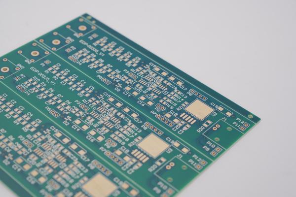
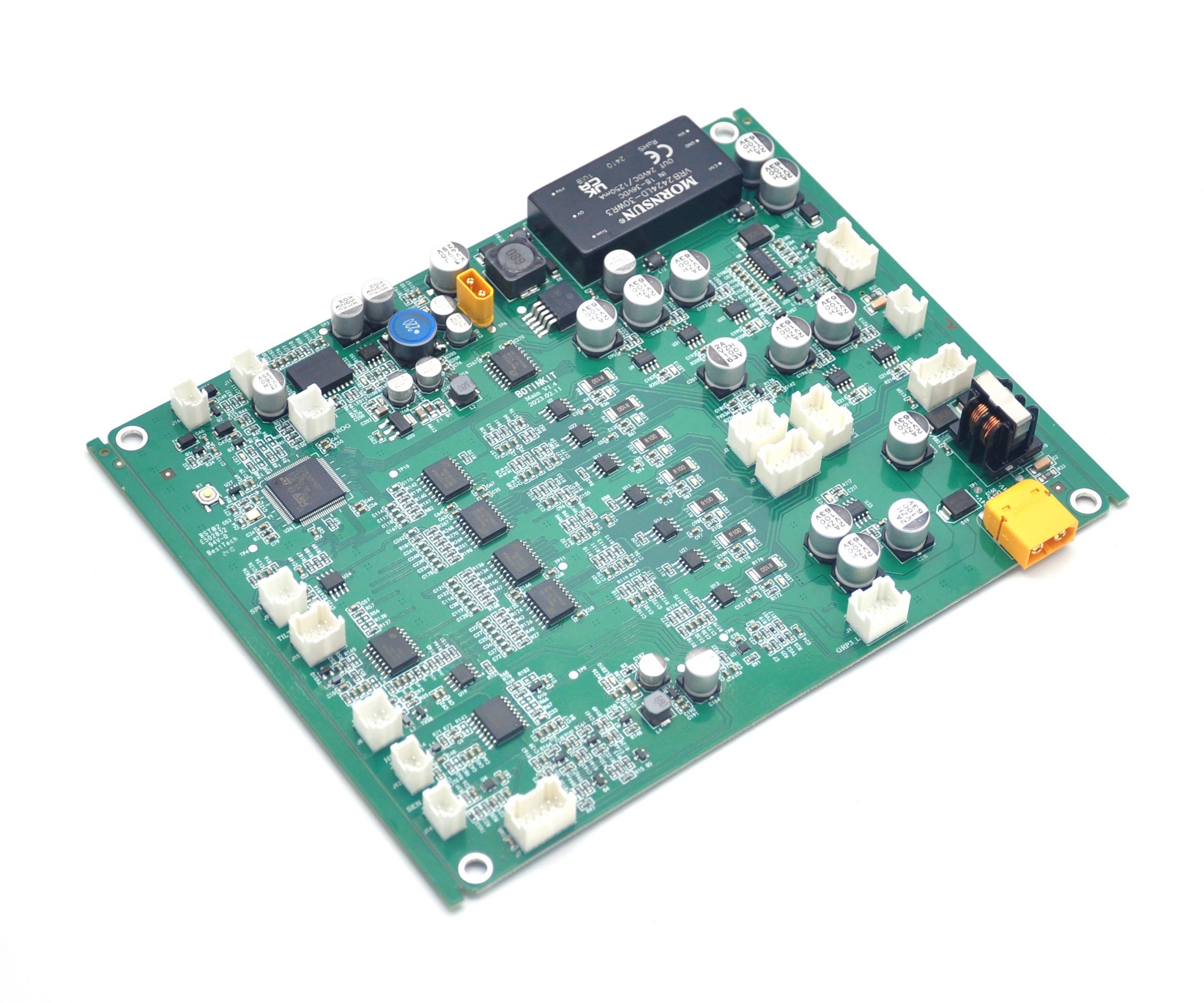
PCB solder plays a vital role in the assembly and function of PCBs. Reliable solder joints must remain intact to prevent components from loosening or falling off the PCB. Solder is the material used to connect the various electronic components on the PCB. Its importance is reflected in several key aspects. Solder ensures that electronic components can be firmly attached to the PCB.
What type of solder for PCB?
The commonly used types of solder for PCB include solder paste, tin bar and tin wire.
- 1. Solder paste: Mainly used in reflow soldering process. Solder paste consists of tin powder, flux and other additives. Tin powder is usually an alloy of tin and other metals. According to different melting points, solder paste can be divided into three types: low temperature, medium temperature and high temperature; according to different lead content, it can be divided into lead solder paste and lead-free solder paste. Lead-free solder paste gradually replaces lead solder paste to reduce environmental pollution.
- 2. Solder bar: Mainly used in wave soldering process. Tin bar (solder bar) has excellent antioxidant ability, good fluidity after melting, suitable for wave soldering process, and is widely used in PCBA processing due to its good fluidity and strong solderability.
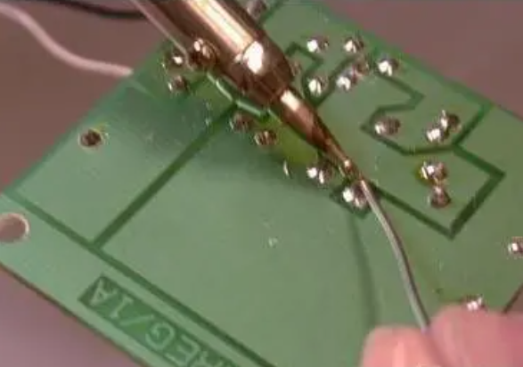
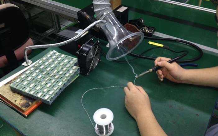
- 3. Tin wire: Mainly used in post-soldering process. Similar to tin bar, tin wire is also a kind of welding material, mainly used for manual welding or other occasions where filament solder is required.
In addition, the selection of welding materials also involves the selection of solder alloys. Eutectic alloys are one of the preferred solder alloys because of their low melting point, low welding temperature, small crystal grains, and dense structure, which are conducive to improving the strength of solder joints.
What temperature should solder be for PCB?
The solder temperature of PCB should vary according to different types of components and welding processes.
For lead-containing PCB boards, the temperature in the preheating stage is usually controlled at 80~120℃ for 1~3 minutes; the temperature in the insulation stage is 150~180℃ for 30~60 seconds; the temperature in the reflow stage is 210~240℃ for 20~40 seconds; the cooling stage speed should be controlled within the range of 4~6℃ per second.
For lead-free PCB boards, the temperature in the preheating stage is usually controlled at 100~150℃, the insulation stage is 180~220℃, the reflow stage is 240~260℃, and the cooling speed should be controlled within the range of 3~5℃ per second.
What is the best soldering temperature for PCB?
The best soldering temperature range for PCB is usually between 240 and 280 degrees Celsius. This temperature range is suitable for manual soldering and can ensure the best soldering effect and component reliability.
For different types of welding situations, the temperature requirements are different:
- 1. Wave soldering: The optimal temperature is 280 degrees Celsius, ensuring that the solder joint temperature is 50 degrees Celsius higher than the melting point of the solder to achieve reliable welding results.
- 2. Small components (such as resistors and capacitors below 1206, and components with an area of less than 5 mm²): The recommended temperature is 250 degrees Celsius to prevent damage to the circuit board.
- 3. Large components: The soldering iron temperature should be set between 350 and 370 degrees Celsius, and the maximum should not exceed 390 degrees Celsius. The welding time should be kept within a few seconds to prevent damage to the pads on the PCB.
- 4. SMT processing: The recommended manual soldering temperature range is 240 to 280 degrees Celsius. Try to minimize the gap between the set temperature and the actual working temperature to achieve the best welding effect and component reliability.
In addition, the precise management of temperature during the welding process is also required to ensure the quality of the solder joints and circuit performance of the PCB board.
- The preheating stage is very important to reduce the thermal shock during welding. The preheating temperature is usually controlled between 80 and 120 degrees Celsius for 1 to 3 minutes.
- The insulation stage is to fully melt the components and solder paste on the PCB board. The temperature is usually controlled between 150 and 180 degrees Celsius for 30 to 60 seconds.
- The cooling stage is to avoid thermal stress caused by rapid cooling. The cooling rate should be controlled to drop between 4 and 6 degrees Celsius per second.
What temperature does PCB solder melt?
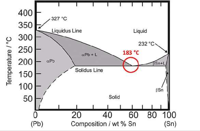
The melting temperature of PCB solder depends on the type of solder. The melting temperature of lead solder ranges from 183°C to 217°C, while the melting temperature of lead-free solder is usually between 217°C and 257°C.
Lead solder has a lower melting point, usually between 183°C and 217°C. During the reflow process, the preheating temperature of lead solder is controlled at 80°C to 120°C, the holding temperature is 150°C to 180°C, the reflow temperature is 210°C to 240°C, and the cooling rate decreases by 4°C to 6°C per second.
The melting point of lead-free solder is higher, usually between 217°C and 257°C. During the reflow process, the preheating temperature of lead-free solder is controlled at 100°C to 150°C, the holding temperature is 180°C to 220°C, the reflow temperature is 240°C to 260°C, and the cooling rate decreases by 3°C to 5°C per second.
What is the melting point of PCB material?
The melting point of PCB material depends on its specific composition and type, usually between 1064℃ and 900℃. For PCB substrate materials, such as FR-4, its temperature resistance is measured by the Tg value (glass transition temperature). Ordinary FR-4 sheets have lower heat resistance, while high TG FR-4 sheets have better heat resistance and can withstand higher temperatures.
Different types of PCB materials have different melting points and heat resistance. The long-term working temperature of ordinary FR-4 sheets is generally between 130℃ and 140℃, and the instantaneous temperature resistance can reach 150℃ to 260℃. In contrast, PCBs made of special materials such as polyimide can withstand higher temperatures, even up to 280℃.
In addition, the surface treatment layer material of the PCB will also affect its heat resistance. For example, the melting point of the gold plating layer depends on the composition of the metal material used.
Which solder is best for PCB?
Choosing a solder suitable for PCB requires comprehensive consideration of multiple factors. The following solders have their own advantages and disadvantages:
- Tin-silver-copper (SAC) alloy: good mechanical and electrical properties, high reliability, suitable for a variety of welding processes, and environmentally friendly. But the cost is high and the welding process requirements are high.
- Tin-copper (Sn-Cu) alloy: low cost, good solderability, and environmentally friendly. The disadvantage is that the mechanical properties are slightly worse in high-demand scenarios.
What type of solder should not be used with electronics?
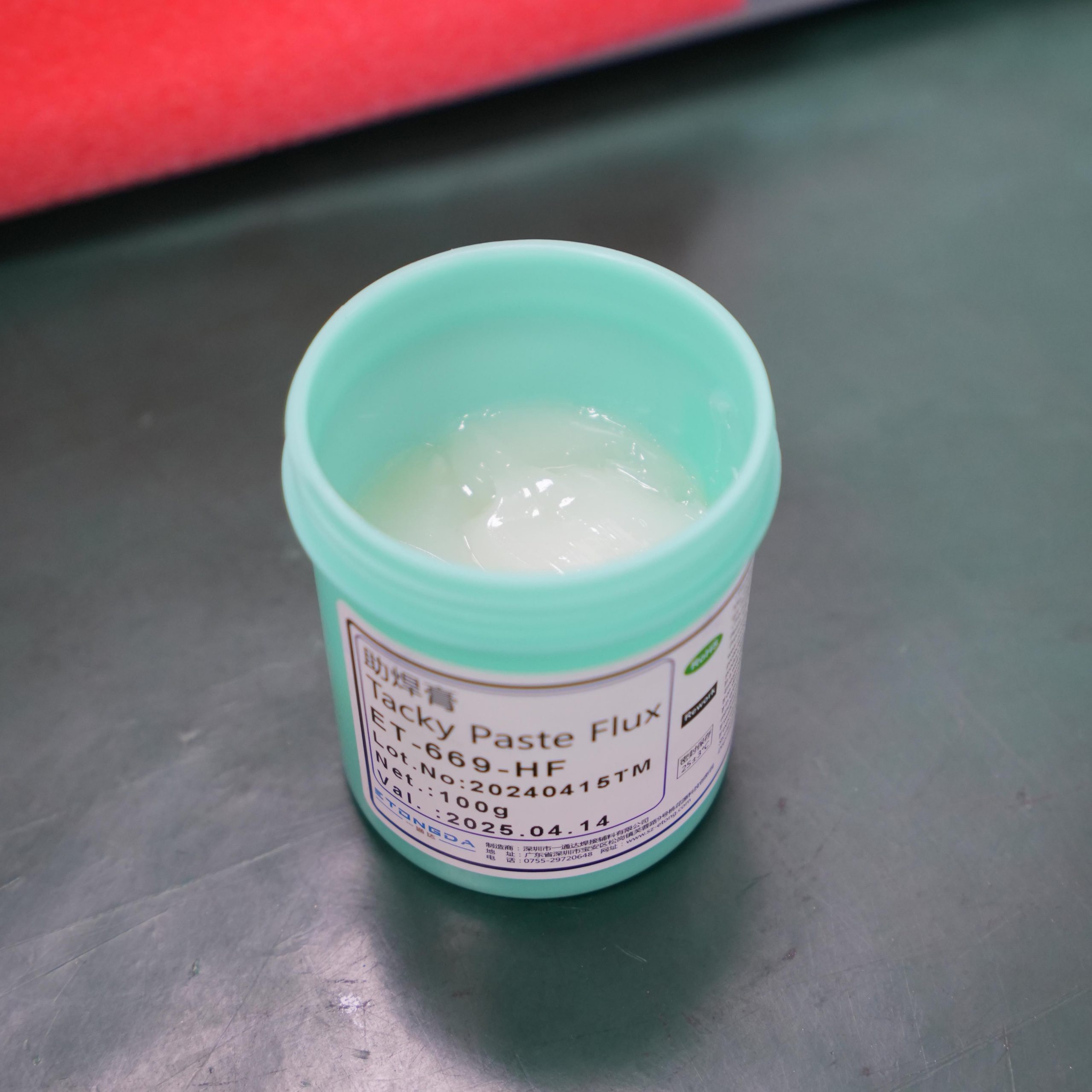
Electronic products should not use strong alkali, rosin grease, coconut oil, and neutral flux as flux.
In the soldering process of electronic products, it is very important to choose a suitable flux. The main function of the flux is to remove the oxide film, prevent oxidation, and improve the quality of soldering.
However, some substances are not suitable for use as flux. Strong alkali and rosin grease will corrode the soldering joint and affect the quality of soldering. In addition, the use of acidic flux will also corrode the soldering joint, so acidic flux should be avoided.
In order to ensure the smooth progress of the soldering process and ensure the quality of soldering, some measures can be taken.
First, choose lead-free solder materials that meet ROHS standards to reduce environmental pollution. Second, use high-brightness soldering iron tips, reduce the use of soldering oil and rosin, and reduce smoke generation. Finally, select appropriate welding materials and processes according to specific needs, such as solder wire, solder paste, solder sheet, etc., to ensure the mechanical and electrical performance of welding.
In short, solder is a key element in the PCB assembly process. Its quality is directly related to whether the electronic equipment can operate normally, and the characteristic of solder melting point plays a decisive role in the welding process. I must deeply study and understand the characteristics of solder to ensure that every solder joint can meet the highest standards.