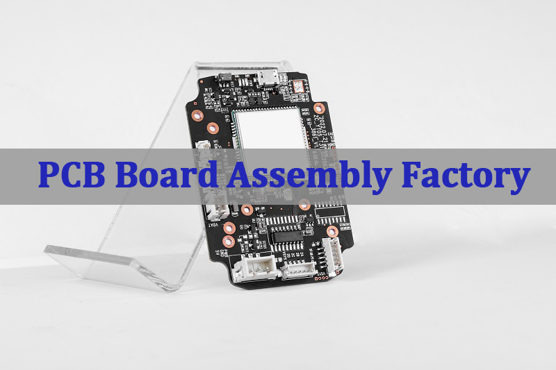
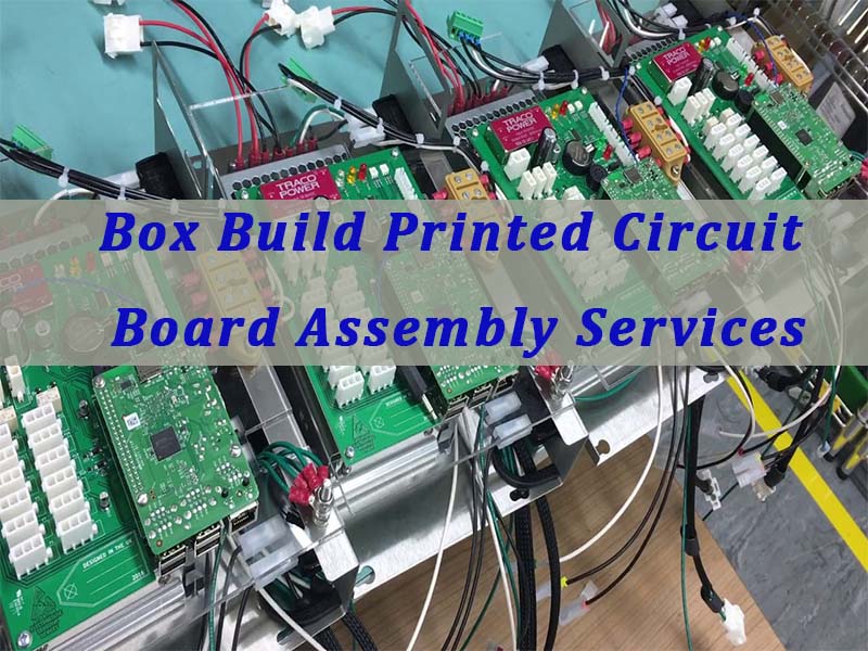
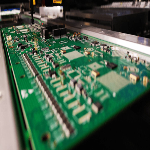
Box build printed circuit board assembly services play a critical role in modern electronics manufacturing by integrating PCB fabrication, component assembly, mechanical enclosure installation, wiring harnesses, and system testing into a single streamlined production process. This article explains how box build PCBA works, what technologies and engineering parameters are involved, and how to choose a reliable manufacturing partner for complete electronic product integration.
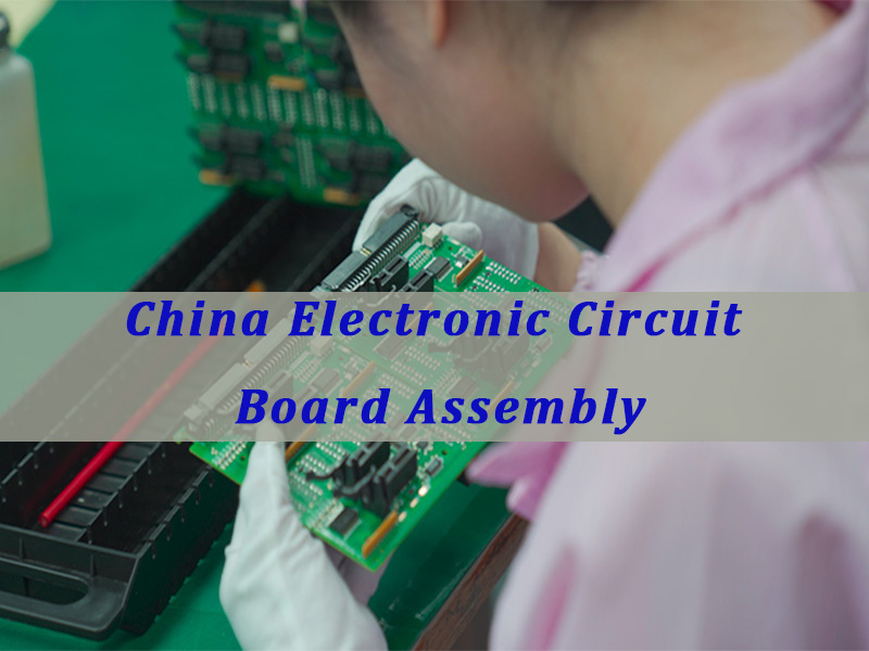
EBest Circuit (Best Technology) is an experienced provider of box build printed circuit board assembly services, offering a one-stop solution that covers PCB fabrication, component sourcing, PCBA manufacturing, wiring harness assembly, and full product integration. With more than 20 years of industry mileage, and certifications including ISO9001, ISO13485, IATF16949, and AS9100D, EBest supports demanding projects from industries such as medical devices, industrial control, and aerospace. If you are looking for reliable box build printed circuit board assembly services to support your next electronics project, feel free to contact our engineering team at sales@bestpcbs.com for professional assistance and a fast quotation.
What Are Box Build Printed Circuit Board Assembly Services?
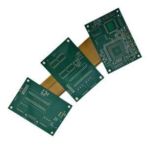
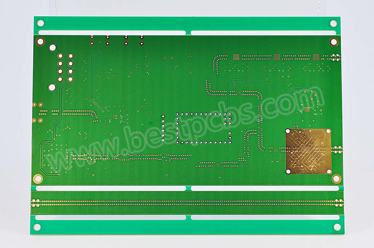
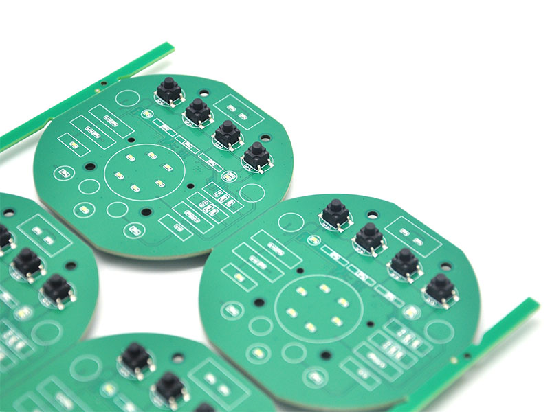
Box build printed circuit board assembly services refer to a complete manufacturing process that integrates PCB fabrication, component assembly, wiring, enclosure installation, and final product testing.
Unlike standard printed circuit board assembly services, which only assemble electronic components onto a PCB, box build services deliver a fully integrated electronic system.
Typical processes involved in box build manufacturing include the following stages.
| Manufacturing Stage | Key Function |
|---|---|
| PCB Fabrication | Bare PCB manufacturing |
| Component Procurement | Authorized component sourcing |
| SMT Assembly | Automated surface-mount placement |
| Through-Hole Assembly | Power and connector soldering |
| Cable Harness Assembly | Wiring and cable integration |
| Mechanical Assembly | Mounting PCBA into enclosure |
| System Integration | Installing modules and subsystems |
| Functional Testing | Electrical and system verification |
| Final Packaging | Labeling and shipment preparation |
This comprehensive workflow allows printed circuit board pcb assembly services to evolve from simple board assembly to complete electronic product integration.
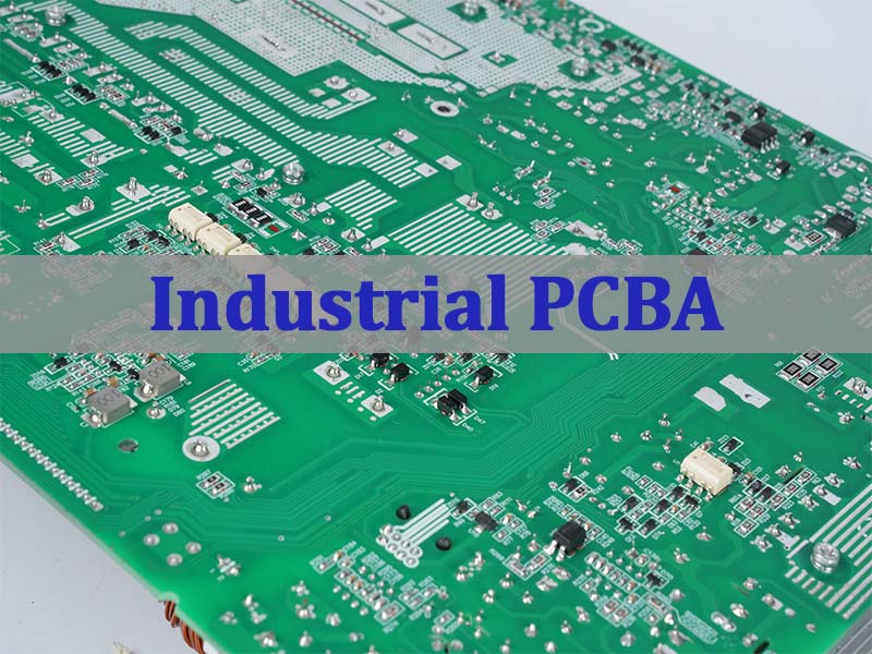
What Processes Are Included in Printed Circuit Board Assembly Services?
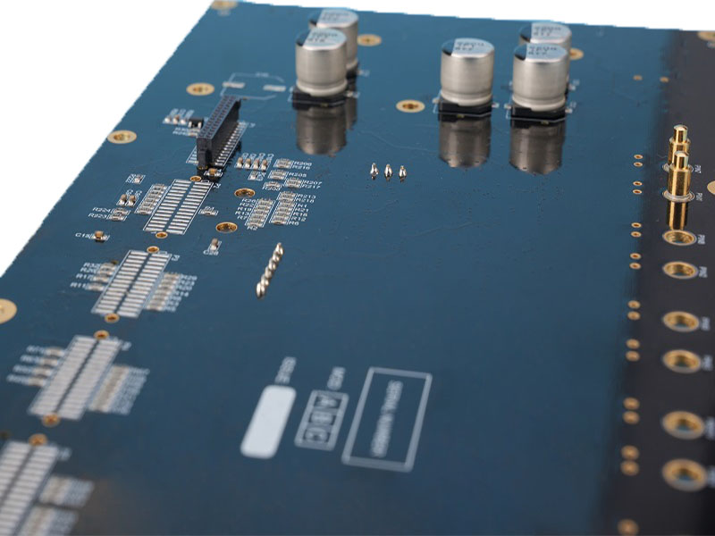
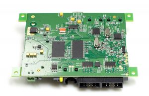
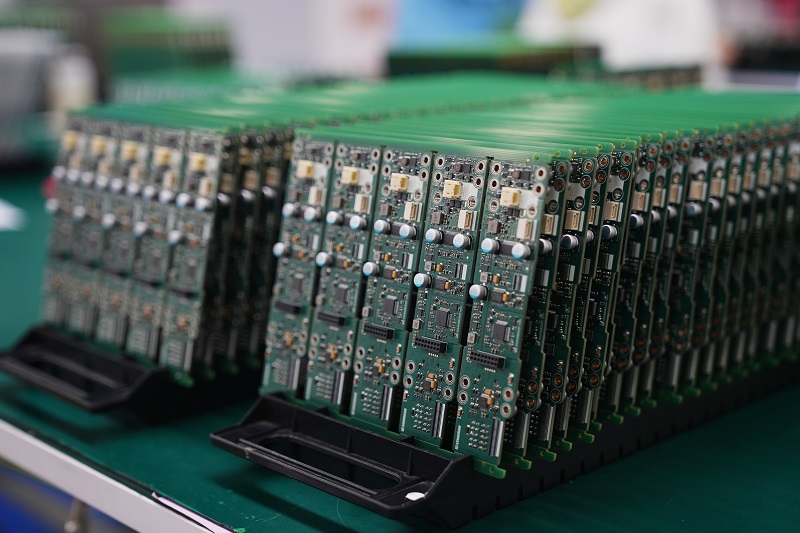
At the core of box build printed circuit board assembly services lies professional PCBA manufacturing. Reliable circuit board assembly services typically include several key production technologies.
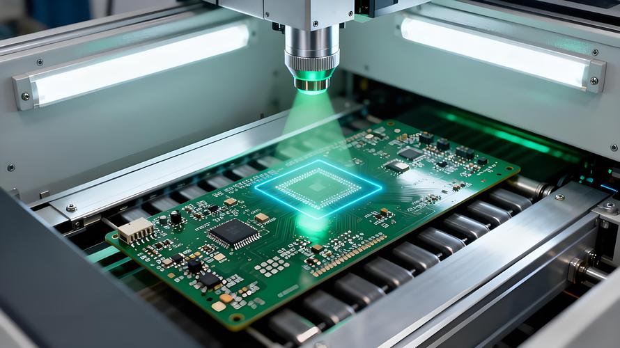
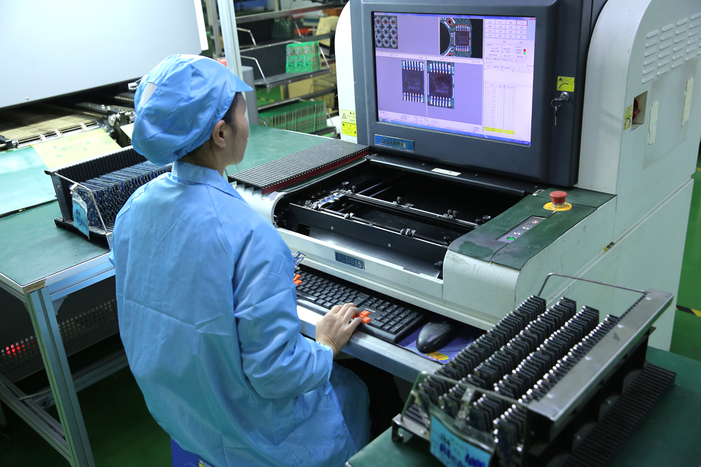
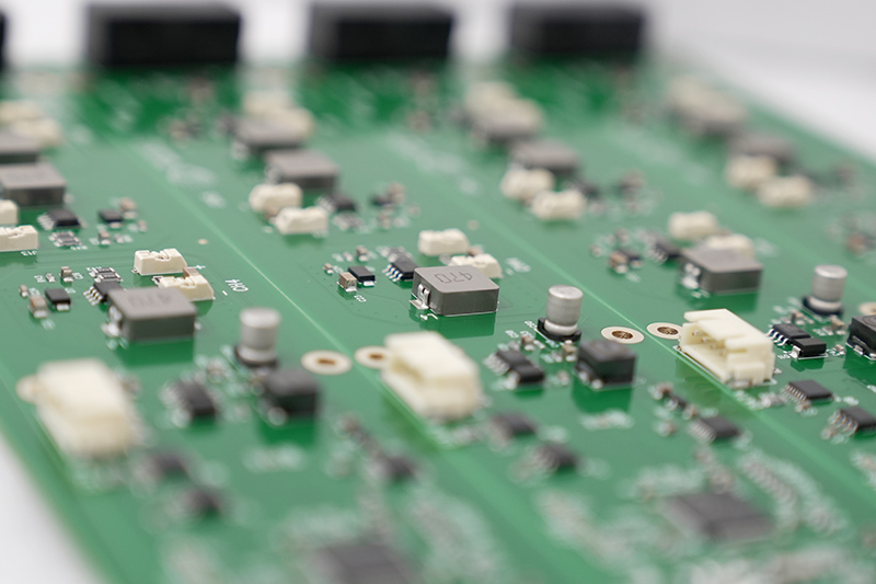
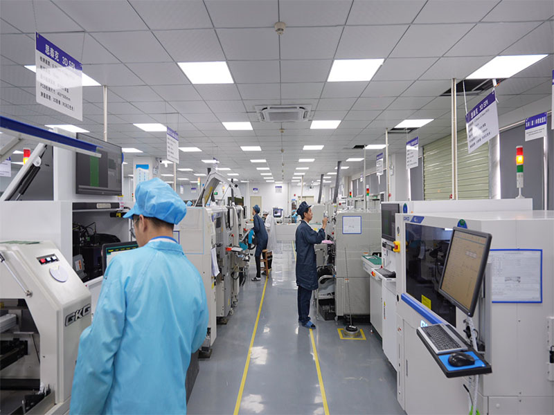
Surface Mount Technology (SMT)
SMT is the primary assembly method used in modern electronics manufacturing. In this process, miniature electronic components are mounted directly onto PCB pads using automated placement machines.
The typical SMT workflow includes:
- Solder paste printing
- High-speed component placement
- Reflow soldering
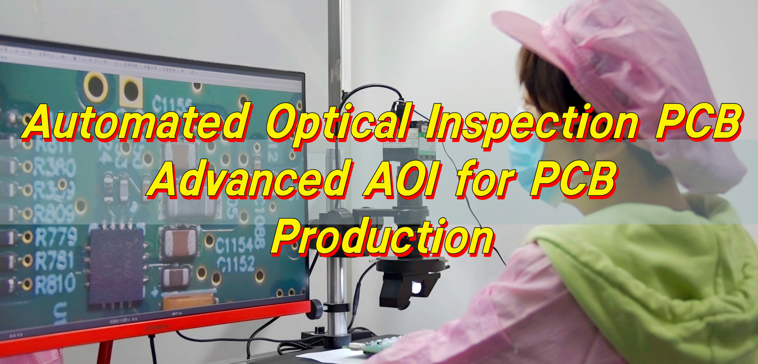
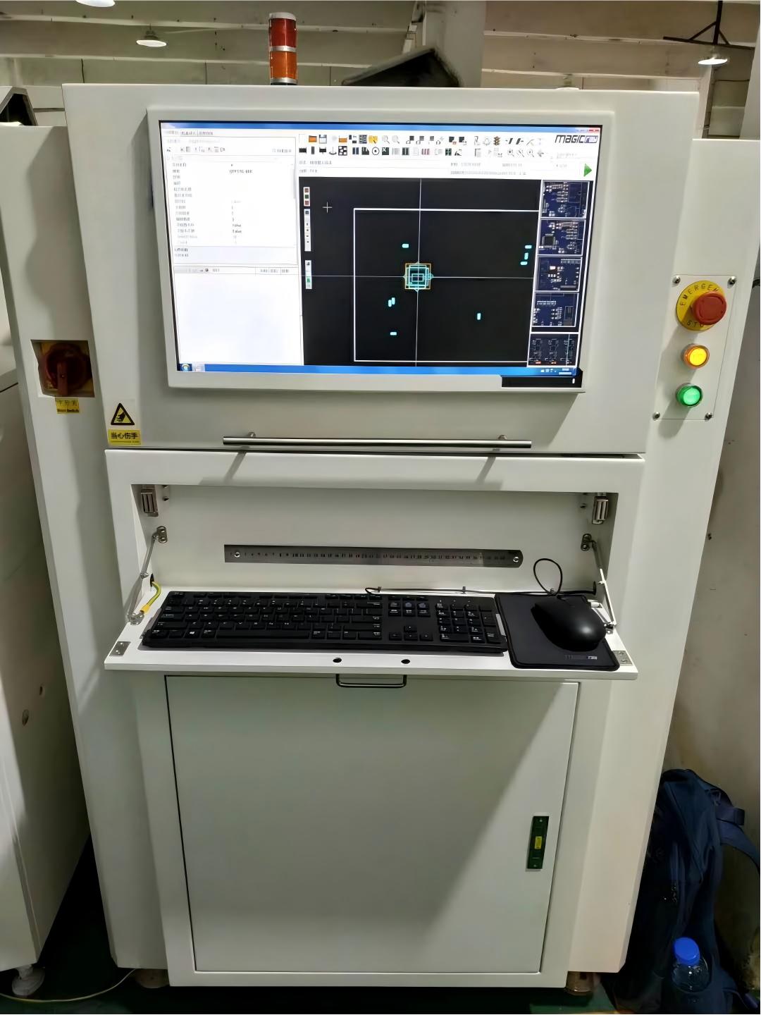
- Automated optical inspection (AOI)
Advanced SMT production lines can place more than 50,000 components per hour, ensuring high productivity and precision.
Typical SMT assembly capabilities are shown below.
| Parameter | Typical Capability |
|---|---|
| Minimum component size | 01005 |
| BGA pitch | 0.3 mm |
| Placement accuracy | ±30 μm |
| Maximum PCB size | 600 × 500 mm |
| Minimum PCB thickness | 0.4 mm |
These capabilities are commonly required in quick turn printed circuit board assembly services for prototypes and small batch production.
Through-Hole Technology (THT)
Although SMT dominates modern electronics manufacturing, many components still require through-hole mounting for mechanical strength or high current handling.
Examples include:
- Power connectors
- transformers
- large electrolytic capacitors
- mechanical switches
These components are soldered using:
- wave soldering
- selective soldering
- manual soldering for complex assemblies
Combining SMT and THT ensures both electrical performance and mechanical reliability in printed circuit board assembly service operations.
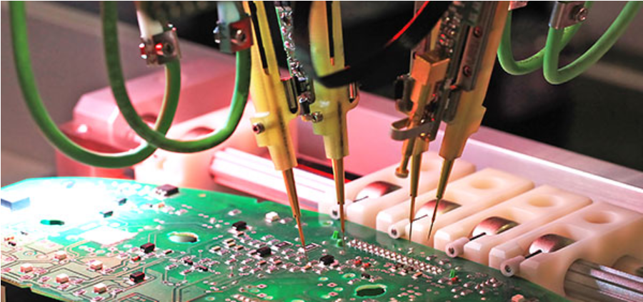
PCBA Testing and Inspection
Testing is critical to ensure the quality and reliability of printed circuit board assembly services.
Common inspection and testing technologies include:
| Test Method | Function |
|---|---|
| AOI | Detects solder bridges, polarity errors, and missing components |
| X-Ray Inspection | Verifies hidden solder joints such as BGA connections |
| ICT (In-Circuit Test) | Checks electrical continuity and component values |
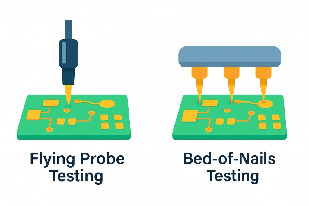
| Flying Probe Test | Used for prototypes without test fixtures |
| Functional Test | Simulates real operating conditions |
Advanced printed circuit board assembly services USA providers often integrate MES systems to maintain full production traceability.
What Technical Parameters Define High-Quality Box Build PCBA?
Beyond assembly processes, several engineering parameters determine the quality and reliability of box build printed circuit board assembly services.
PCB Current Carrying Capacity
The current capacity of a PCB trace depends on copper thickness, trace width, and temperature rise.
A simplified formula derived from IPC-2152 is:
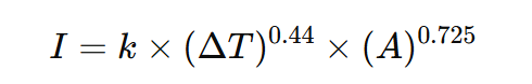
Where:
| Symbol | Meaning |
|---|---|
| I | Current capacity (Amps) |
| ΔT | Temperature rise |
| A | Cross-section area of copper |
| k | Constant depending on layer type |
For example, a 1 oz copper trace with a width of 20 mil typically carries around 2–3 A depending on cooling conditions.
This parameter becomes particularly important in industrial control box build systems where power modules are integrated.
Signal Integrity and Impedance Control
High-speed digital signals require controlled impedance traces to avoid signal reflection and distortion.
Typical impedance targets include:
| Interface Type | Typical Impedance |
|---|---|
| USB differential pair | 90 Ω |
| Ethernet | 100 Ω |
| RF signal lines | 50 Ω |
| LVDS | 100 Ω |
A simplified microstrip impedance equation is:
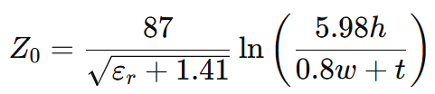
Where:
- (ε_r) is dielectric constant
- (h) is dielectric thickness
- (w) is trace width
- (t) is copper thickness
Professional printed circuit board pcb assembly services verify impedance using TDR testing.
Thermal Resistance of Electronic Components
Thermal performance is another critical engineering parameter.
The junction temperature of a semiconductor can be estimated using:
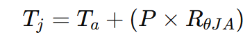
Where:
| Symbol | Meaning |
|---|---|
| Tj | Junction temperature |
| Ta | Ambient temperature |
| P | Power dissipation |
| RθJA | Thermal resistance |
Example:
If a device dissipates 5W, with thermal resistance 20°C/W, and ambient temperature 40°C, then:
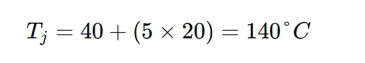
Such temperature levels require improved thermal management solutions.
How Does Box Build Assembly Work in Electronics Manufacturing?
While printed circuit board assembly services focus on electronic boards, box build integrates the entire product.
A typical workflow includes:
| Step | Process |
|---|---|
| 1 | PCB fabrication |
| 2 | PCBA assembly |
| 3 | wiring harness preparation |
| 4 | enclosure installation |
| 5 | power module integration |
| 6 | system wiring |
| 7 | functional testing |
| 8 | final packaging |
A typical box build structure may include the following subsystems.
| Subsystem | Example Components |
|---|---|
| Control board | MCU PCBA |
| Power module | DC-DC converters |
| Interface board | Ethernet or USB modules |
| Mechanical enclosure | Aluminum chassis |
| Cooling system | Heat sink or fan |
| Wiring harness | Signal and power cables |
This integrated approach allows assembly services for circuit boards to deliver complete electronic products.
Thermal Management Design in Box Build Electronics
Thermal management is a key engineering challenge in box build printed circuit board assembly services, particularly when electronics operate in enclosed environments.
Aluminum PCB for Heat Dissipation
Different PCB materials provide different thermal conductivity.
| Material | Thermal Conductivity |
|---|---|
| FR-4 | 0.3 – 0.4 W/mK |
| Aluminum PCB | 2 – 3 W/mK |
| Copper base PCB | 5 – 8 W/mK |
Aluminum PCBs are widely used in:
- LED lighting systems
- power electronics
- automotive electronics
Heat Sink Design
Heat dissipation through convection can be estimated using:
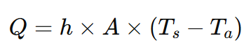
Where:
| Symbol | Meaning |
|---|---|
| Q | Heat transfer |
| h | Heat transfer coefficient |
| A | Surface area |
| Ts | Surface temperature |
| Ta | Ambient temperature |
This formula helps engineers design efficient cooling structures for high-power electronic systems.
Forced Air Cooling
When power density exceeds 10 W per PCB, passive cooling may be insufficient.
In such cases, engineers may integrate:
- cooling fans
- ventilation openings
- heat pipes
These solutions are common in industrial and telecom box build systems.
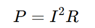
What Industries Need Box Build Printed Circuit Board Assembly Services?
Many industries rely on box build printed circuit board assembly services for complete product integration.
Industrial Automation
Industrial control equipment often includes:
- controller PCBs
- sensor interface boards
- power control modules
- display units
Box build simplifies system integration.
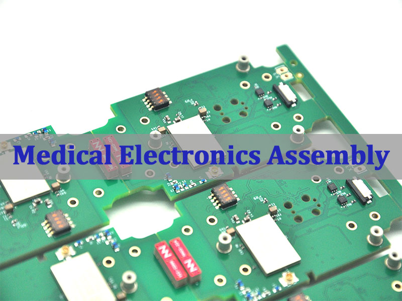
Medical Electronics
Medical devices require:
- strict quality control
- traceability
- reliable electronics
Integrated printed circuit board assembly services ensure regulatory compliance.
IoT Devices
IoT products combine:
- wireless modules
- sensors
- batteries
- compact enclosures
Box build allows these devices to be delivered as fully assembled products.
Automotive Electronics
Automotive modules often integrate:
- multilayer PCBs
- aluminum heat sinks
- sealed housings
- wiring harnesses
Box build assembly ensures these components operate reliably under harsh environments.
What Is the Difference Between PCBA and Box Build Assembly?
The difference between PCBA and box build lies in the level of integration.
| Manufacturing Type | Description |
|---|---|
| PCBA | Assembly of electronic components onto a PCB |
| Box Build | Full product assembly including enclosure, wiring, and system integration |
In many cases, box build printed circuit board assembly services combine both processes to deliver complete electronic products.
How to Choose a Reliable Printed Circuit Board Assembly Service Provider?
Selecting a manufacturer for printed circuit board assembly services california, the USA, or overseas requires evaluating several factors.
Important considerations include:
- engineering support and DFM analysis
- advanced SMT manufacturing capability
- strong component sourcing network
- complete testing and inspection systems
- box build integration capability
A supplier capable of providing quick turn circuit board assembly services USA or Asia-based rapid manufacturing can significantly shorten product development cycles.
Why Work With a Professional Box Build PCBA Manufacturer?
A professional partner offering box build printed circuit board assembly services should provide both manufacturing capability and engineering expertise.
For example, EBest Circuit (Best Technology) provides:
- over 20 years of PCB and PCBA manufacturing experience
- free DFM analysis and BOM optimization
- rapid quick turn printed circuit board assembly services
- certifications including ISO 9001, ISO 13485, IATF 16949, and AS9100D
- advanced MES system for full production traceability
These capabilities enable reliable printed circuit board assembly services for industries such as industrial automation, medical electronics, and aerospace systems. If you are looking for reliable box build printed circuit board assembly services, feel free to contact our engineering team at sales@bestpcbs.com.
FAQs About Box Build Printed Circuit Board Assembly Services
What is included in printed circuit board assembly services?
Typical services include component sourcing, SMT assembly, through-hole soldering, testing, and inspection.
How long does quick turn circuit board assembly take?
Prototype quick turn printed circuit board assembly services typically take 3–7 days, depending on PCB complexity and component availability.
Are China printed circuit board assembly services reliable?
Many china printed circuit board assembly services providers operate advanced SMT factories and follow international quality standards.
What industries commonly use box build manufacturing?
Industries such as industrial automation, medical electronics, telecommunications, and IoT hardware frequently use box build assembly services.