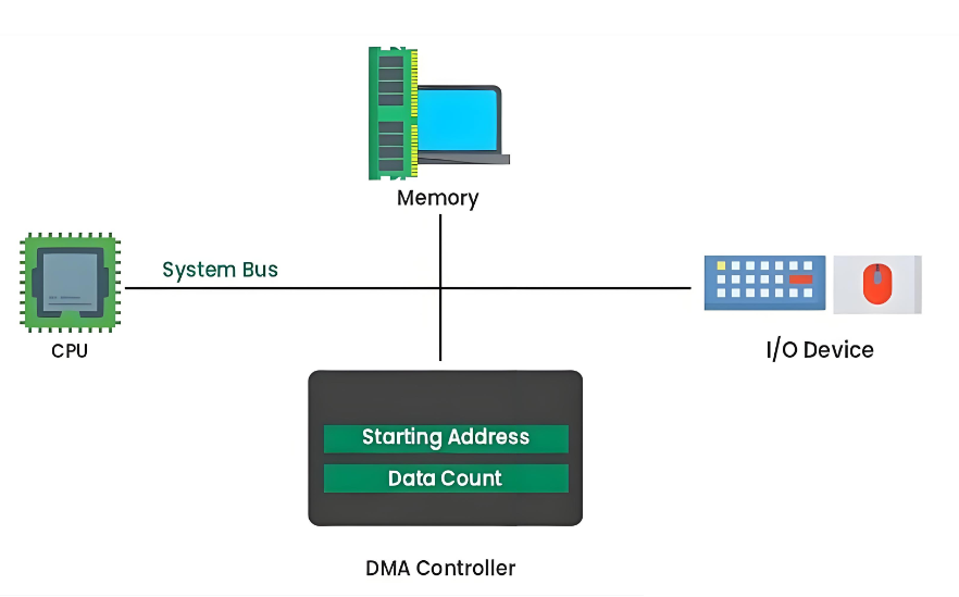
What Is Direct Memory Access (DMA)?
Direct Memory Access (DMA) is a hardware mechanism that moves data between memory and peripherals with minimal CPU involvement. The CPU still orchestrates DMA (configures addresses, sizes, modes, and permissions), but the DMA engine performs the bulk transfer over the system interconnect.
For an electronic engineer, the most useful mental model is: DMA is a bus master (or a bus client with granted master capability) that can read/write memory and peripheral registers/FIFOs under strict rules set by software. In a well-designed system, DMA increases throughput, reduces latency jitter, and frees the CPU for control and signal-processing work.
Why DMA Was Introduced in Computer Systems?
DMA exists because CPU-driven I/O is structurally wasteful:
- CPU copy loops burn cycles, create cache pressure, and increase interrupt frequency.
- Peripheral interfaces (ADC, SPI, SDIO, Ethernet MAC, USB, PCIe endpoints) produce/consume data faster than it is efficient for the CPU to babysit.
- Real-time systems require predictable timing; heavy polling or frequent interrupts can destabilize deadlines.
DMA addresses these by shifting “data movement” to dedicated hardware and letting the CPU focus on scheduling, protocol handling, and application logic.
How DMA Works Step by Step?
A typical transfer (microcontroller or SoC) looks like this:
1. Allocate a buffer in RAM and decide ownership rules (who writes, who reads, when).
2. Program the DMA channel: source address, destination address, transfer length, width, burst size, increment modes, and trigger source (timer, peripheral request line, or software trigger).
3. Arm/enable DMA and the peripheral (e.g., enable UART RX DMA, start ADC, enable SPI TX DMA).
4. DMA arbitrates for the bus, then performs reads/writes in bursts.
5. DMA signals completion via interrupt, event flag, or callback; optionally it can trigger a half-transfer event for streaming.
6. Software post-processes data (parse packets, filter samples, enqueue buffers) and re-arms DMA if needed.
If you design embedded firmware, the real craft is not the register writes; it is the buffer lifecycle, coherency, and error handling.
What is DMA used for?
DMA is used whenever data volume, rate, or determinism makes CPU-driven transfers inefficient. It is widely used in:
- ADC sampling into circular buffers for DSP, FFT, or control loops
- UART/SPI/I²C continuous RX/TX without byte-by-byte interrupts
- Audio I²S/SAI streaming with ping-pong buffers
- Storage (SDMMC, NAND, QSPI) block moves into RAM
- Networking (Ethernet MAC) RX/TX descriptor rings
- Display pipelines (LCD/DSI) frame buffer fetch
- FPGA or high-speed sensor capture where sustained bandwidth matters
A practical heuristic: if you are handling sustained streams above a few tens of kB/s (platform-dependent) or you need tight jitter bounds, DMA is usually worth it.
What are the three types of DMA?
These three “types” are commonly taught because they map well to bus usage and CPU impact.
- Burst Mode DMA
DMA takes the bus and transfers a block (or large burst) with minimal interruption. Throughput is high, but CPU and other masters may be stalled or delayed depending on arbitration priority.
- Cycle Stealing DMA
DMA transfers one unit (or small burst), then releases the bus, interleaving with CPU cycles. This improves responsiveness at the cost of peak throughput.
- Transparent DMA
DMA transfers only when the CPU is not using the bus (or during “idle slots”). It minimizes CPU interference but can starve the transfer if the CPU is busy.
DMA vs CPU-Based Data Transfer
When the CPU handles data transfer directly, it must read and write every data unit. This process consumes clock cycles and reduces overall system efficiency.
DMA eliminates this bottleneck by enabling parallel operation. While the DMA controller moves data, the CPU continues executing other tasks, improving throughput and multitasking capability. Here is a detailed comparison between them:
| Dimension | CPU Copy | DMA |
| CPU utilization | High | Low–Medium (setup + ISR) |
| Peak throughput | Limited by CPU + bus | Limited mostly by bus + DMA |
| Jitter in real-time tasks | Often worse | Often better (if designed correctly) |
| Complexity | Low | Medium–High |
| Failure modes | Obvious | Subtle (alignment, coherency, ownership) |
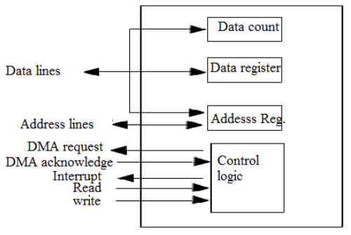
Key Components of a DMA Controller
Most DMA implementations (MCU or SoC) contain:
- Channels/streams: independent transfer engines (or time-sliced engines)
- Request routing: connects peripheral request lines to channels
- Address generators: increment/fixed addressing, wrap/circular modes
- Transfer sizing: byte/halfword/word, burst length
- Descriptors/LLI (linked lists): scatter-gather, chained transfers
- Status/interrupt logic: half-transfer, complete, error, FIFO threshold
- Arbitration/QoS: priority levels, bandwidth caps, fairness rules
On higher-end SoCs, DMA is often split into specialized blocks: PDMA (peripheral DMA), XDMA (general), GPDMA, MDMA, or dedicated engines for Ethernet, USB, and display.
DMA in Embedded Systems and Microcontrollers
DMA is a staple in embedded design because it turns “interrupt-per-byte” into “interrupt-per-buffer.”
1) Circular buffers for streaming
A common pattern is circular DMA into a ring buffer, with half-transfer and full-transfer interrupts:
- Half-transfer ISR: process first half while DMA fills second half
- Full-transfer ISR: process second half while DMA wraps to first half
This provides steady throughput and predictable CPU load.
2) Ping-pong buffers
For bursty traffic or strict processing windows (audio frames, sensor blocks), use two buffers:
- DMA fills Buffer A while CPU processes Buffer B
- Swap on completion
Ping-pong is often simpler to validate than a large ring, especially when you must guarantee “no overwrite before consume.”
3) UART RX DMA for robust logging and protocols
UART is notorious for ISR overhead at high baud rates. RX DMA into a ring buffer plus an “IDLE line” interrupt (common on many MCUs) is a strong combination:
- DMA continuously writes bytes
- IDLE interrupt fires when line quiets
- CPU reads DMA write pointer and parses frames
Practical guidance: treat your DMA write index as the source of truth; avoid “guessing” byte counts.
DMA in Modern Operating Systems
In modern OS environments, DMA is not optional—it is foundational.
Descriptor rings and zero-copy paths
Network drivers, NVMe, and many high-speed devices use descriptor rings:
- Driver posts buffer descriptors (physical addresses, lengths, flags)
- Device DMA-writes received data directly into buffers
- Driver later hands buffers to the stack or application
The most performance-critical paths aim for zero-copy, where data is not copied again in software unless necessary.
IOMMU and protection
On PCs/servers, devices can DMA into memory. To control this safely, platforms use an IOMMU (Intel VT-d / AMD-Vi style conceptually):
- It maps device-visible addresses to physical memory
- It prevents devices from DMA-reading/writing arbitrary memory
- It enables safe virtualization and isolation
As an engineer, the important takeaway is: DMA is powerful enough to be a security boundary, so modern systems gate it with hardware translation and permissions.
Advantages of DMA
- Lower CPU overhead and reduced interrupt pressure
- Higher sustained throughput for streaming I/O
- Better timing stability for control loops and real-time workloads
- Enables architectures like descriptor rings and pipeline processing
Limitations of DMA
- Cache coherency: CPU cache may not match RAM content DMA reads/writes
- Alignment and width constraints: some DMA engines require aligned addresses or specific transfer widths
- Buffer ownership bugs: CPU modifies a buffer while DMA is still using it
- Bus contention: DMA can starve other masters or create latency spikes
- Error visibility: misconfiguration can fail silently until timeouts appear
DMA makes data movement fast, but it makes system correctness a discipline.
FAQs
1. Is DMA always faster than CPU copying?
Often, yes for sustained transfers, but not universally. For very small copies, CPU might be faster due to setup overhead. The crossover point depends on bus speed, DMA engine capability, cache behavior, and interrupt frequency.
2. What is the most common DMA bug in embedded projects?
Cache coherency and buffer ownership. Engineers frequently forget to clean/invalidate caches (on systems with data cache) or accidentally reuse a buffer before DMA completes.
3. Do microcontrollers have cache coherency issues too?
Some do, some do not. Many MCUs lack data cache, making coherency simpler. Higher-performance MCUs and SoCs frequently include caches, which makes coherency a first-class design concern.
4. What is scatter-gather DMA and why do engineers use it?
Scatter-gather DMA uses linked descriptors to move non-contiguous memory segments without CPU intervention. It’s essential for networking, storage, and any system that uses buffer chains efficiently.
5. How do I decide between circular DMA and ping-pong buffers?
Use circular DMA for continuous streams where you can tolerate ring semantics and want minimal reconfiguration. Use ping-pong when you need strict “block-by-block” processing with clear ownership boundaries.
6. Can DMA corrupt memory?
Yes, if misconfigured or if address boundaries are wrong. That is why robust drivers validate lengths, alignment, region permissions, and use memory protection where available.
7. Does DMA bypass the CPU in a security sense?
In many architectures, DMA can access memory without CPU executing loads/stores. That is why platforms use IOMMU-like controls, MPU regions, or DMA address filters to limit what DMA can touch.