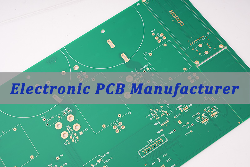
When you’re looking for reliable China PCB assembly and manufacturing factories, EBest is your ultimate choice. With over 20 years of expertise in PCB manufacturing and assembly China, we deliver turnkey solutions that solve your core pain points, ensure top-tier quality, and guarantee on-time delivery. Whether you need small-batch customization, urgent prototyping, or large-scale mass production, EBest stands out among China PCB assembly and manufacturing suppliers as the most trusted partner for global clients.

Are You Facing these Challenges of PCB Manufacturing and Assembly China?
- Inconsistent product quality: Many China PCB and assembly manufacturer cut corners on raw materials or process control, leading to PCB failures (e.g., copper foil peeling, impedance mismatch) that affect end-product performance.
- Unreliable delivery times: Delays due to poor supply chain management or inefficient production processes disrupt clients’ project timelines and increase costs.
- Lack of one-stop service: Needing to cooperate with multiple vendors for PCB design, fabrication, component sourcing, and assembly creates communication gaps and process inefficiencies.
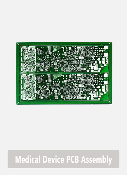
- Inability to handle complex requirements: Most PCB and assembly manufacturer in China fail to meet the strict technical standards for high-precision PCBs (e.g., HDI, extra thin PCB) used in medical, aerospace, and industrial equipment.
- No transparent production traceability: Without a professional tracking system, clients cannot monitor production progress or verify process compliance, leading to quality risks.
- Poor technical support: Lack of professional engineers to provide DFM (Design for Manufacturability) analysis results in design flaws that cause production delays and cost overruns.
- Inability to meet industry-specific certifications: Many suppliers lack the necessary certifications for medical, aerospace, or automotive PCB manufacturing, making their products unqualified for these sectors.
Turnkey Solutions for PCB Manufacturing and Assembly We Offer
When navigating PCB manufacturing and assembly China, you need a strategic partner who understands your challenges and delivers tangible results. As a leading China PCB and assembly manufacturer, EBest’s turnkey one-stop services eliminate inefficiencies common with ordinary China PCB assembly and manufacturing suppliers, delivering cost savings and faster time-to-market while maintaining top quality.
To solve the pain point of fragmented vendor coordination, our integrated turnkey solution covers the entire PCB lifecycle. Key solutions include: end-to-end service from design optimization to final assembly and testing, PCB manufacturing and assembly China consolidating all your needs under one roof, and eliminating communication gaps and wasted time from juggling multiple vendors. This streamlines your process, cuts extra costs and delays, letting you focus on product innovation and business growth.
To fix inconsistent product quality, we implement a rigorous quality assurance system. Our specific solutions: use only high-grade certified raw materials from trusted global suppliers, conduct full-process inspections at every production stage, and deploy advanced testing equipment operated by seasoned engineers. These steps ensure your PCBs meet strict specifications for medical, aerospace or industrial use, with no costly reworks.
For reliable delivery, we’ve built a robust system to avoid project delays. Our solutions include: optimize supply chain management with long-term partnerships with trusted material suppliers, real-time production tracking via our advanced MES system, 24-hour urgent prototyping service for tight deadlines, and flexible scheduling to accommodate both small-batch prototypes and large-scale production.
To enhance your overall PCB manufacturing and assembly China experience, we add value with key support services: free DFM (Design for Manufacturability) analysis to optimize your designs before production, full production traceability to verify compliance at every step, and 24/7 multilingual technical support from our professional engineering team.
Why Choose EBest for China PCB Manufacturing and Assembly Factory?
Our advantages are tailored to your needs, focusing on efficiency, quality, and cost-saving, making us the top PCB fabrication and assembly manufacturer in China:
- One-stop service: Save time and cut communication costs by letting us handle every stage of your PCB manufacturing and assembly China project from PCB design, prototyping, and fabrication to component sourcing, assembly, and testing. You’ll avoid the hassle of coordinating multiple vendors and reduce the risk of delays or miscommunication.
- Free DFM analysis: Protect your budget and keep projects on track with free DFM (Design for Manufacturability) analysis from our professional engineers. We identify design flaws early and optimize for manufacturability, eliminating costly rework, production delays, and wasted resources.
- MES system traceability: Gain full peace of mind with our advanced MES system, which tracks every production step from raw material input to final delivery. This transparency lets you monitor progress in real time, verify process compliance, and mitigate quality risks for your PCB manufacturing and assembly China orders.
- 24-hour urgent prototyping: Keep your project timeline on track even with tight deadlines. Our expedited 24-hour prototyping service ensures your PCB prototypes are shipped within a day, so you can accelerate product development and get to market faster.
- Small-batch customization: No MOQ (minimum order quantity) requirement means you can order as few as 1 piece—perfect for startups, R&D projects, or small-scale trials. This flexibility reduces your initial investment and lets you test ideas without unnecessary costs.
- 20+ years of expertise: Benefit from our deep industry knowledge, gained from serving global clients since 2006. We understand the unique PCB manufacturing and assembly requirements of medical, aerospace, and industrial equipment sectors, ensuring your PCBs meet strict industry standards.
- Multilingual technical support: Get fast, efficient solutions to your technical questions with 24/7 multilingual support from our professional engineers. No more language barriers or long wait times, we’re here to keep your projects moving smoothly.
What Types of China PCB Manufacturing and Assembly Services Can We Provide?
As a reliable China PCB manufacturing and assembly manufacturer, we offer a full range of services to meet diverse industry needs, including:
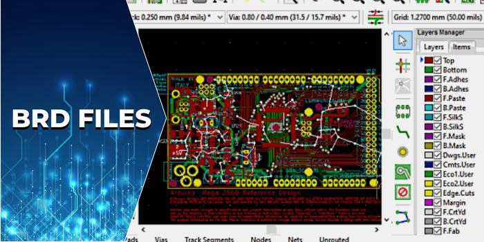
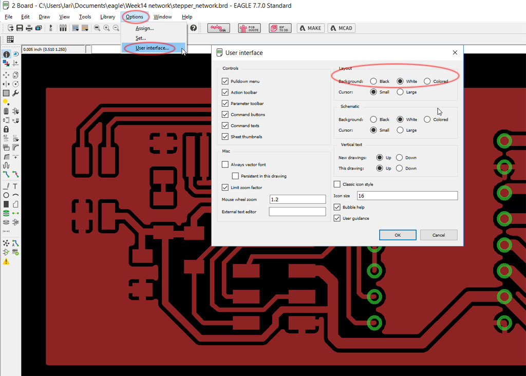
- PCB Design: Custom design services tailored to your product requirements, including schematic design, PCB layout, and DFM optimization.
- PCB Prototype: Rapid prototyping for all PCB types, with 24-hour urgent service and strict quality testing to ensure prototype accuracy.
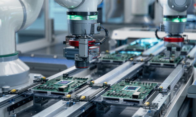
- Mass Production: Large-scale production with stable quality and high efficiency, supporting monthly output of 260,000 square feet.
- Component Sourcing: Reliable component sourcing from certified suppliers, ensuring genuine parts and stable supply.
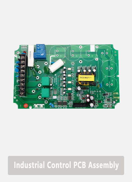
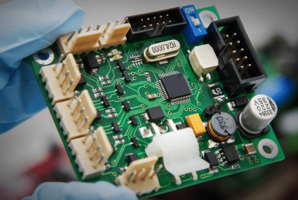
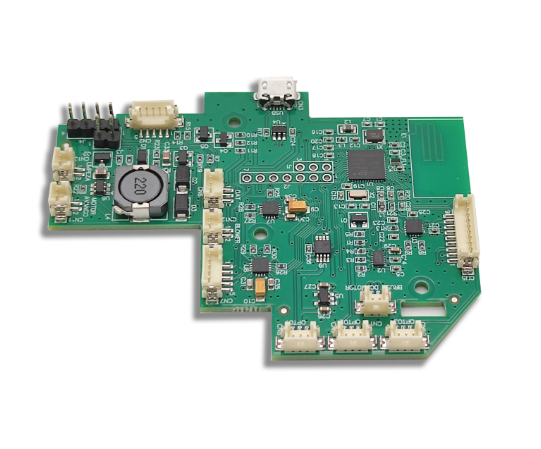
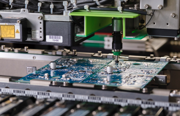
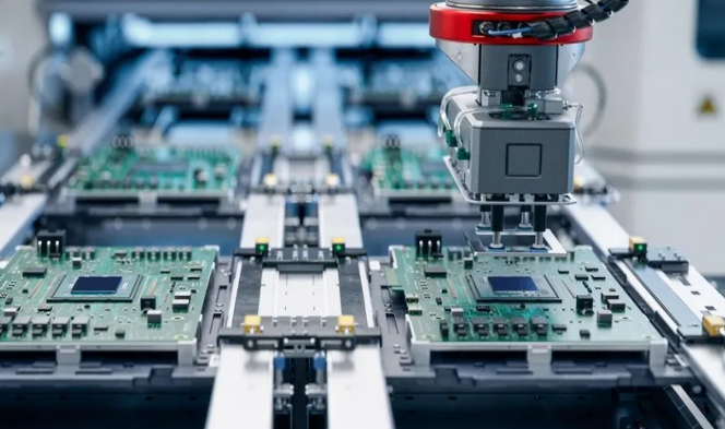
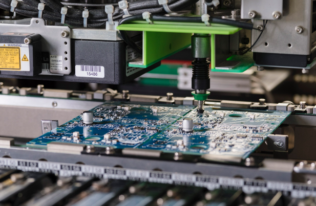
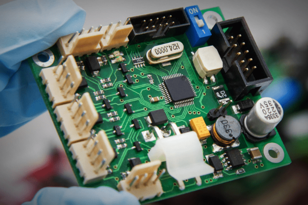
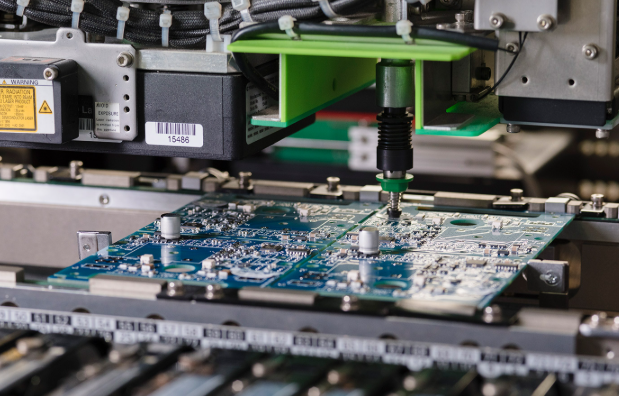
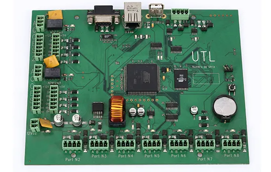
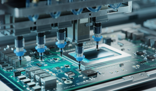
- PCB Assembly: SMT (Surface Mount Technology) and through-hole assembly, with precision placement and soldering to meet industry standards.
- Testing Services: Comprehensive testing, including flying probe testing, functional testing, impedance testing, and thermal testing, to ensure PCB performance.
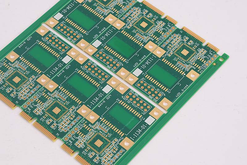
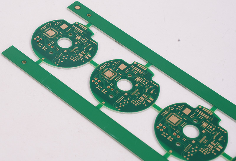
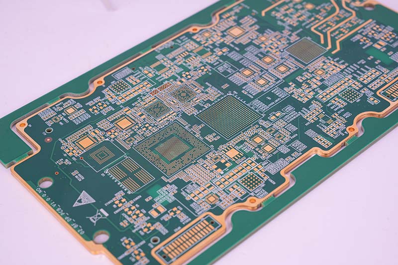
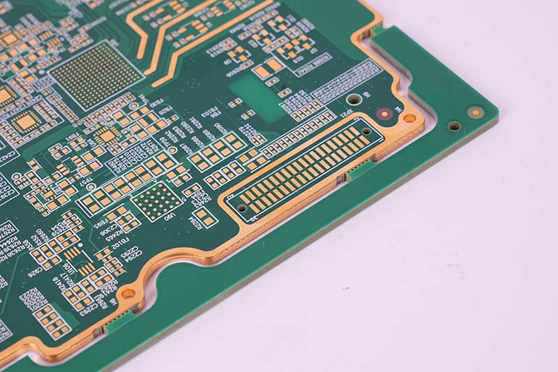
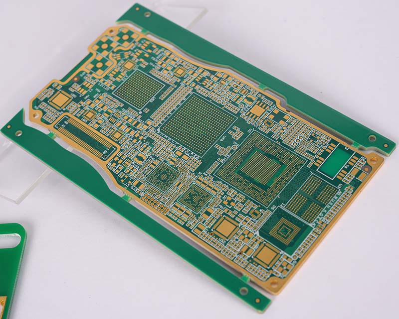
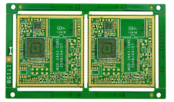
- Custom PCB Fabrication: Specialized fabrication for various PCB types, including HDI, heavy copper, high-frequency, ceramic, and rigid-flex PCBs.
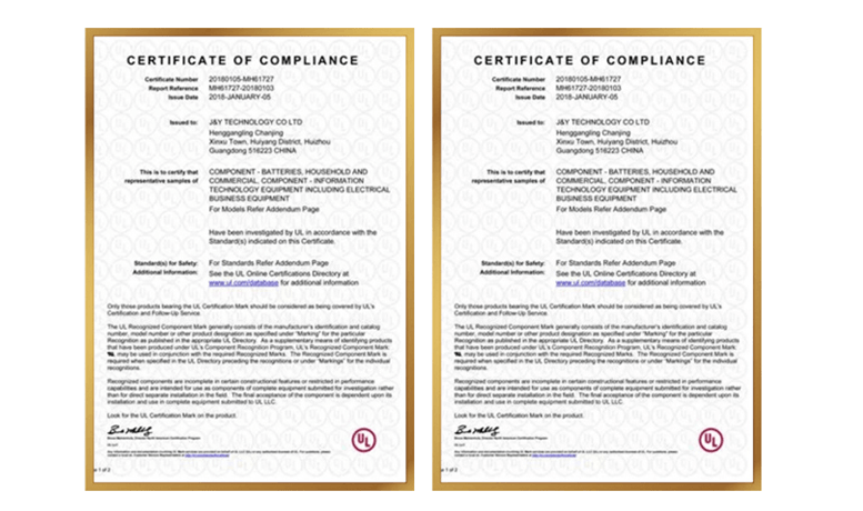
What Quality Certifications Has EBest Obtained for China PCB Manufacturing and Assembly?
Below are quality certifications for China PCB manufacturing and assembly orders we have:
- IATF 16949: For automotive PCB manufacturing, ensuring compliance with automotive industry quality standards.
- ISO 9001:2015: General quality management system certification, ensuring consistent product quality and service.
- ISO 13485:2016: For medical PCB manufacturing, meeting the strict quality requirements of the medical device industry.
- AS9100D: For aerospace PCB manufacturing, complying with aerospace industry standards for reliability and safety.
- REACH: Compliance with EU regulations on chemical substances, ensuring our PCBs are safe for global markets.
- RoHS: Compliance with EU RoHS directives, restricting hazardous substances in electronic products.
- UL: Safety certification for electronic components, ensuring our PCBs meet global safety standards.
Our Quality Inspection Processes for China PCB Manufacturing and Assembly Orders
Incoming Material Inspection (IQC – Incoming Quality Control)
- All raw materials (copper clad laminates, solder masks, solder pastes, components) undergo rigorous testing against international standards (e.g., IPC-4101 for laminates, J-STD-006 for solder).
- Certificates of compliance (CoC) and material safety data sheets (MSDS) are verified.
- Critical parameters like thickness, dielectric constant, and thermal conductivity are measured using precision instruments.
In-Process Inspection (IPQC – In-Process Quality Control)
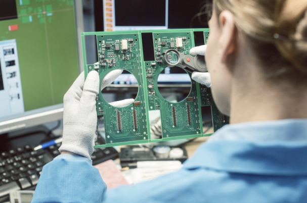
- Automated Optical Inspection (AOI): Post-etching, post-solder mask, and post-soldering stages are inspected for defects (e.g., shorts, opens, misalignment).
- X-ray Inspection: For BGA/QFN components to verify solder joint integrity and void analysis.
- Flying Probe/ICT Testing: Electrical continuity and functionality checks during assembly.
- Process Audits: Regular checks on operator adherence to SOPs (Standard Operating Procedures) and process parameters (e.g., temperature, pressure).
Final Quality Control (FQC)
- Visual Inspection: 100% board-level inspection for cosmetic defects (e.g., scratches, delamination) per IPC-A-600 standards.
- Functional Testing: Full electrical testing (e.g., voltage, current, signal integrity) using automated test equipment (ATE).
- Burn-In Testing: Accelerated life testing to identify early-life failures (e.g., thermal cycling, power cycling).
Reliability and Environmental Testing
- Thermal Shock/Cycle Testing: -40°C to +125°C cycles to simulate extreme temperature changes.
- Vibration/Shock Testing: Compliance with IEC 60068-2-6 (vibration) and IEC 60068-2-27 (shock).
- Humidity/Salt Spray Testing: For corrosion resistance (e.g., 85°C/85% RH for 168 hours, salt spray per ASTM B117).
Packaging and Shipping Inspection
- ESD-Safe Packaging: Anti-static bags, moisture barrier bags (MBBs), and desiccants to prevent electrostatic discharge (ESD) and humidity damage.
- Labeling Compliance: RoHS/REACH compliance labels, part numbers, batch codes, and country-of-origin marking.
- Shipping Audits: Random checks for packaging integrity and documentation (e.g., packing lists, certificates of conformance).
Documentation and Traceability
- Batch Records: Detailed logs of material lots, machine settings, operator IDs, and test results.
- Traceability Systems: Serialization and QR codes for end-to-end traceability from raw materials to finished goods.
- Certificates of Analysis (CoA): Issued for each shipment, detailing test results and compliance with customer specifications.
Continuous Improvement and Customer Collaboration
- Statistical Process Control (SPC): Real-time monitoring of critical process parameters (e.g., Cp/Cpk for capability analysis).
- 8D/Corrective Action Reports (CAR): Root cause analysis for defects and preventive measures.
- Customer Audits: Open access for customer quality audits and joint process improvement initiatives.

How Do We Ensure On-Time Delivery of PCB Manufacturing and Assembly Orders in China?
On-time delivery is critical for your project success, and EBest has established a robust system to ensure 97% on-time delivery rate for PCB manufacturing and assembly China orders:
- Advanced Production Scheduling: We leverage intelligent scheduling software to optimize every production plan. This ensures we use our equipment and personnel efficiently, eliminating bottlenecks and keeping your PCB manufacturing and assembly China order on track from start to finish.
- Robust Supply Chain Management: We’ve built long-term partnerships with reliable raw material and component suppliers. This stable supply network prevents delays caused by material shortages, ensuring your PCB production never gets held up.
- MES System Real-Time Tracking: Our advanced MES system lets us monitor your order’s production progress in real time. We can spot potential delays early and take prompt corrective actions, keeping you informed and your project on schedule.
- 24/7 Production Capacity: Our facilities operate around the clock, 24 hours a day, 7 days a week. This allows us to handle urgent orders efficiently and meet even the tightest deadlines for your PCB manufacturing and assembly China needs.
- Flexible Production Lines: We have dedicated production lines for small-batch, large-scale, and urgent orders. This separation ensures each order is processed efficiently, with no interference, and delivered on time, regardless of size or urgency.
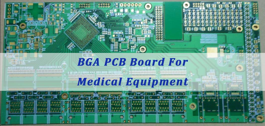
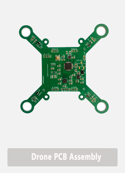
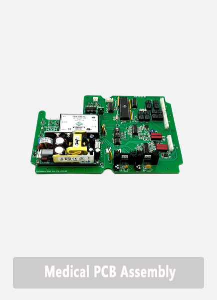
Case Study: Medical PCB Production and Assembly for Cardiac Monitoring Device
Project Background
A leading European medical device manufacturer required high-precision PCBs for a next-generation cardiac monitoring system. The device needed to operate in extreme conditions (-40°C to +85°C) while maintaining 99.9% signal integrity over a 10-year lifecycle. The client chose our China-based facility due to our ISO 13485 certification, IPC Class 3 compliance, and proven track record in medical electronics.
Project Requirements
- Technical Specifications: 12-layer HDI PCB with 0.08mm line/space, blind/buried vias, and ENIG surface finish.
- Reliability Standards: Pass IEC 60601-1 (medical electrical equipment safety), MIL-STD-883 (thermal cycling), and ASTM F1979 (thermal shock).
- Performance Metrics: ≤0.1dB signal loss across 1-10GHz bandwidth, ≤1μV noise floor, and 100% electrical continuity.
Project Challenges
- Microvia Reliability: 0.08mm laser-drilled microvias required <1% voiding in solder joints (measured via X-ray inspection).
- Thermal Management: High-power components demanded thermal conductivity ≥3.0 W/mK in substrate materials.
- ESD Sensitivity: Medical-grade components required <100V ESD protection during assembly.
Our Solutions
Material Selection: Rogers 4350B laminates with optimized dielectric constant (Dk=3.48±0.03) and low loss tangent (Df=0.0037).
Process Innovation:
- AOI systems with 5μm resolution for post-etching defect detection (reduced false rejects by 15%).
- X-ray inspection with 3D CT scanning for BGA solder joint analysis (achieved 99.8% voiding compliance).
- Vacuum reflow ovens with O2 <100ppm for void-free soldering.
Reliability Testing:
- 1,000 thermal cycles (-55°C to +125°C) with <5% resistance change.
- 48-hour salt spray testing (ASTM B117) with zero corrosion.
Project Outcomes
- Quality Metrics: 99.7% first-pass yield (up from client’s previous 92% supplier average).
- Cost Efficiency: 25% cost reduction through optimized material usage and automated testing.
- Delivery Performance: 14-day lead time (vs. industry average of 21 days) with 100% on-time delivery.
FAQs About PCB Manufacturing and Assembly China
Q1: What is the minimum order quantity (MOQ) for your PCB manufacturing and assembly China services?
A1: We have no MOQ requirement. We support small-batch orders (even 1 piece) for prototypes and R&D projects, as well as large-scale mass production. This flexibility helps startups and small businesses reduce initial costs, while meeting the needs of large enterprises for scalable production.
Q2: How long does it take to get a prototype for PCB manufacturing and assembly China?
A2: We offer 24-hour urgent prototyping service for simple PCBs (1-2 layers, FR4). For complex PCBs (multi-layer, HDI, high-frequency), the prototype lead time is 3-5 days. We prioritize urgent orders to ensure your project stays on track.
Q3: Can you handle custom PCB designs for medical and aerospace industries?
A3: Yes. We have rich experience in custom PCB design and manufacturing for medical, aerospace, and industrial equipment industries. Our team of professional engineers can optimize your design for manufacturability, and we hold ISO 13485, AS9100D, and IATF 16949 certifications to meet industry-specific requirements.
Q4: How do you ensure the quality of PCB manufacturing and assembly China orders?
A4: We implement a strict quality control process covering raw material inspection, in-process inspection, post-assembly testing, and final quality audit. We use advanced testing equipment and hold multiple quality certifications to ensure every PCB meets your specifications and global standards. Our MES system also provides full production traceability for transparency.
Q5: Do you provide DFM analysis for PCB manufacturing and assembly China?
A5: Yes, we provide free DFM analysis for all orders. Our engineers will review your PCB design to identify potential flaws (e.g., incorrect hole size, impedance mismatch) and optimize it for manufacturability, reducing rework, delays, and costs.
How to Get a Quote for China PCB Assembly and Manufacturing Service?
Ready to kickstart your pcb manufacturing and assembly china project with a fair, accurate quote—one that saves you time, cuts costs, and aligns perfectly with your goals? Don’t wait to move your project forward, please send your requirements to our dedicated sales team today via email: sales@bestpcbs.com — Your first step toward a seamless, high-quality PCB manufacturing experience.
To get a tailored quote fast (and avoid costly guesswork), include these key details: PCB design files (Gerber, PCB file), PCB type (FR4, HDI, ceramic, etc.), layer count, copper thickness, surface finish, order quantity, and any special requirements (certifications, lead time, etc.). Our expert team will respond within 24 hours with a detailed, transparent solution, plus free technical support to help you optimize your project and maximize value. Let’s turn your PCB vision into reality, together.