If you’re knee-deep in the electronics, PCB, or manufacturing world, you’ve probably stumbled across the acronym “ICT” more times than you can count. But what *exactly* does ICT stand for? Is it the same across different industries, or does it have a specific meaning when you’re talking about printed circuit boards (PCBs), assembly, or quality control? Let’s break it down in plain language—no jargon overload, just the facts you need as a tech professional.
The Core ICT Full Form You Need to Know
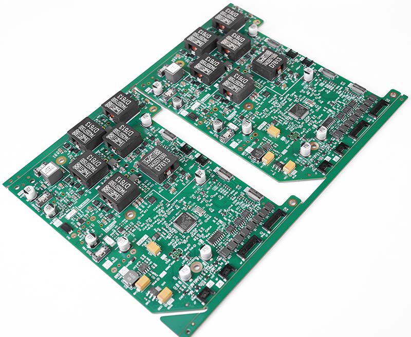
First things first: the most common ICT full form in electronics, manufacturing, and PCB design is In-Circuit Test. This isn’t some vague industry buzzword—it’s a critical process that separates functional products from faulty ones, especially when you’re producing PCBs, assembled components, or complex electronic devices.
While there are other niche meanings (like “Information and Communication Technology” in broader tech contexts), if you’re working with PCBs, component sourcing, or electronic assembly, In-Circuit Test is the ICT definition that matters. It’s the standard term used by engineers, quality inspectors, and manufacturers worldwide—including teams at EBest Technology, where we rely on ICT to ensure every PCB prototype and mass-produced board meets our strict quality standards.
Why ICT (In-Circuit Test) Matters for Your Electronics Projects
You might be thinking: “Do I really need to care about ICT?” The short answer: yes—if you want reliable, high-performance products that don’t fail in the field. Here’s why ICT is non-negotiable:
- Catches defects early: ICT tests individual components and connections on a PCB *before* final assembly. This means you spot issues like soldering errors, missing components, or short circuits early—saving you time, money, and headaches down the line.
- Ensures consistency: For mass production (like our 260,000 square feet monthly PCB capacity at EBest), ICT provides repeatable, accurate testing. No more guessing if a batch of boards is up to spec—ICT verifies every unit.
- Supports compliance: Certifications like IATF 16949 (automotive), ISO 13485 (medical), and AS9100D (aerospace) often require rigorous quality control—and ICT is a key part of meeting those standards.
How ICT Works – A Simplified Explanation
You don’t need a PhD in electrical engineering to understand the basics of ICT. Here’s a quick breakdown:
An ICT system uses a test fixture with pins that make contact with specific points on a PCB (called test points). The system sends small electrical signals through the board to check:
1. If components are correctly placed and soldered.
2. If there are open circuits (broken connections) or short circuits (unintended connections).
3. If component values (like resistors, capacitors) match the design specs.
It’s like giving your PCB a “health checkup” before it’s integrated into a final product. Fast, efficient, and thorough—exactly what you need when you’re dealing with tight deadlines (including our 24-hour expedite service for urgent PCB orders).
ICT vs. Other Common Testing Methods – What’s the Difference?
ICT isn’t the only testing method out there, but it’s one of the most reliable for PCB-based projects. Let’s compare it to two other popular options to help you decide what’s right for your work:
| Testing Method | Key Use Case | Pros | Cons |
|---|---|---|---|
| ICT (In-Circuit Test) | PCB prototypes, mass production, component verification | High accuracy, catches component-level defects, fast for high volumes | Requires test points on the PCB design |
| Functional Test (FT) | Final product validation | Tests how the product works in real-world use | Can’t pinpoint individual component defects |
| Visual Inspection | Quick checks for obvious issues (e.g., missing parts) | Low cost, no special equipment | Misses hidden defects (e.g., internal soldering errors) |
For most PCB projects—whether you’re designing a custom multi-layer PCB or a rigid-flexible PCB—ICT is the best first line of defense against defects.
When to Integrate ICT into Your PCB Project Workflow
Timing is everything when it comes to ICT. Here’s the optimal workflow to maximize its value:
1. PCB Design: Work with your designer to include test points (this is critical—without them, ICT isn’t possible).
2. PCB Prototype: Run ICT on prototypes to validate your design and catch issues before mass production.
3. Mass Production: Implement ICT as part of your quality control process for every batch (we do this for all our PCB assembly and box-build assembly services).
4. Post-Assembly: Use ICT to verify that components are functioning correctly after final assembly.
Common ICT Myths Debunked
There’s a lot of misinformation floating around about ICT. Let’s set the record straight:
- Myth 1: ICT is too expensive for small projects.
Fact: Many ICT systems are scalable—you don’t need a huge setup for prototypes or small batches. At EBest, we offer ICT as part of our PCB prototype and assembly services, so you don’t have to invest in equipment yourself. - Myth 2: ICT slows down production.
Fact: Modern ICT systems test boards in seconds. For mass production, the time saved by catching defects early far outweighs the testing time. - Myth 3: If a PCB passes visual inspection, it doesn’t need ICT.
Fact: Visual inspection misses hidden issues like cold solder joints or faulty components. ICT is the only way to ensure electrical functionality.
FAQ – Your Most Pressing ICT Full Form & Testing Questions Answered
1. What is the most common ICT full form in electronics?
The most common ICT full form in electronics, PCB design, and manufacturing is In-Circuit Test. Other meanings (like Information and Communication Technology) are used in broader tech contexts but aren’t relevant for PCB or assembly work.
2. Do I need to include test points on my PCB for ICT?
Yes—ICT relies on test points to make electrical contact with the board. Work with your PCB designer to include them in the layout; this is a simple step that saves time later.
3. Can ICT test all types of PCBs?
ICT works for most PCB types, including standard FR4 PCBs, multi-layer PCBs, metal-based PCBs (MCPCBs), ceramic PCBs, and rigid-flexible PCBs. We use ICT for all these PCB types at EBest.
4. How long does an ICT test take?
For a single PCB, ICT tests take 10–30 seconds. For mass production batches, the process is automated, so you can test hundreds or thousands of boards per hour.
5. Is ICT required for PCB certifications like ISO 9001 or IATF 16949?
While the certifications don’t explicitly “require” ICT, they do mandate rigorous quality control. ICT is a widely accepted way to meet those requirements, especially for industries like automotive and medical (which require ISO 13485 compliance).
6. Can ICT detect faulty components?
Yes—ICT checks component values, connections, and functionality. If a resistor is out of spec, a capacitor is faulty, or a component is missing, ICT will flag it.
7. Do you offer ICT as part of your PCB services at EBest?
Absolutely. We integrate ICT into our PCB prototype, mass production, and PCB assembly services to ensure every product meets our quality standards and your specifications.
How EBest Technology Uses ICT to Deliver Reliable PCB Solutions
At EBest, we’ve been in the PCB game for over 20 years—so we know that quality starts with rigorous testing. Here’s how we leverage ICT to support our one-stop PCB solutions:
- End-to-end testing: We run ICT on every prototype and production batch, from standard FR4 boards to high-frequency PCBs and custom ceramic PCBs.
- Compliance-focused: Our ICT processes are aligned with global certifications (IATF 16949, ISO 9001:2015, AS9100D) to meet the strictest industry requirements.
- Customized for your needs: Whether you need ICT for a small prototype order or a large-scale mass production run, we tailor our testing to your project’s specs.
- Fast turnaround: Even with ICT testing, we maintain our 24-hour expedite service for urgent orders—no compromise on speed or quality.
Key Considerations When Choosing an ICT-Enabled PCB Partner
Not all PCB manufacturers use ICT effectively. When choosing a partner, look for these red flags (and why EBest checks all the boxes):
- Do they integrate ICT into their workflow? Avoid partners who skip ICT or only offer it as an expensive add-on. We include it as standard for most services.
- Are they certified? Certifications like ISO 9001 and IATF 16949 prove they take quality (and ICT) seriously.
- Can they handle your PCB type? Make sure they use ICT for your specific needs—whether it’s flexible PCBs, MCPCBs, or high-frequency boards.
- Do they offer component sourcing and assembly? A one-stop partner (like EBest) can handle PCB design, prototype, mass production, component sourcing, PCB assembly, and box-build assembly—all with ICT testing built in.
Real-World Example – How ICT Saved a Client’s Project
A few months ago, a client came to us for mass production of 5,000 multi-layer PCBs for an automotive application (requiring IATF 16949 compliance). During our ICT testing phase, we detected a batch of resistors with incorrect values—something that would have caused the PCBs to fail in the field.
Instead of shipping faulty products, we replaced the defective components, re-tested with ICT, and delivered the batch on time. The client avoided costly recalls, maintained their reputation with their automotive partner, and saved thousands in potential damages. That’s the power of ICT—and why we never skip it.
Ready to Work with a PCB Partner That Prioritizes ICT & Quality?
If you’re tired of dealing with faulty PCBs, missed deadlines, or partners who cut corners on testing, it’s time to switch to EBest Technology. We’re a trusted global provider of one-stop PCB solutions with over 20 years of experience, and ICT is at the heart of everything we do.
Whether you need PCB design, a quick prototype, mass production (up to 260,000 square feet monthly), component sourcing, PCB assembly, or box-build assembly—we’ve got you covered. Our team of experts uses ICT to ensure every product meets your specs, complies with global certifications (IATF 16949, ISO 9001:2015, ISO 13485:2016, AS9100D, REACH, RoHS, UL), and performs reliably in the field.
We also offer 24-hour expedite service for urgent orders—because we know deadlines matter. No jargon, no hidden fees, just transparent communication, personalized support, and high-quality PCBs tested with ICT to perfection.
Don’t risk your project with a partner that skips critical testing. Contact EBest Technology today to discuss your PCB needs. Let’s bring your vision to life—with the quality and reliability that only ICT testing can guarantee. We’re ready to be your trusted PCB partner—so reach out now and get started.