Why choose HDI printed circuit board for smart POS? Let’s discover its benefits, applications, technical parameter, how to balance cost and performance, signal integrity optimization solutions for HDI PCB through this blog.
Are you worried about these problems?
- Does your POS mainboard freeze frequently in extreme environments?
- Are traditional PCBs holding back your device’s slim design?
- Poor circuit board reliability driving up after-sales costs?
As a HDI PCB manufacturer, EBest Circuit (Best Technology) can provide you service and solutions:
- High-Stability HDI Stack-up: Materials resistant to low/high temps, reducing failure rates by 60%.
- Any-Layer Interconnect Tech: Enables 0.8mm ultra-thin 8-layer boards.
- Enhanced Surface Treatment: Passes 48-hour salt spray test, doubling product lifespan.
Welcome to contact us if you have any request for HDI printed circuit board: sales@bestpcbs.com.
Why Choose HDI Printed Circuit Board for Smart POS?
Benefits of HDI Printed Circuit Board for Smart POS
- Ultimate Miniaturization: Adopts sub-0.1mm microvias, blind/buried via technology, and thin interlayer dielectric design, boosting wiring density by 30%-50% per unit area. Enables compact integration of multi-modules (processor, communication chip, security chip, etc.) and supports device slimming.
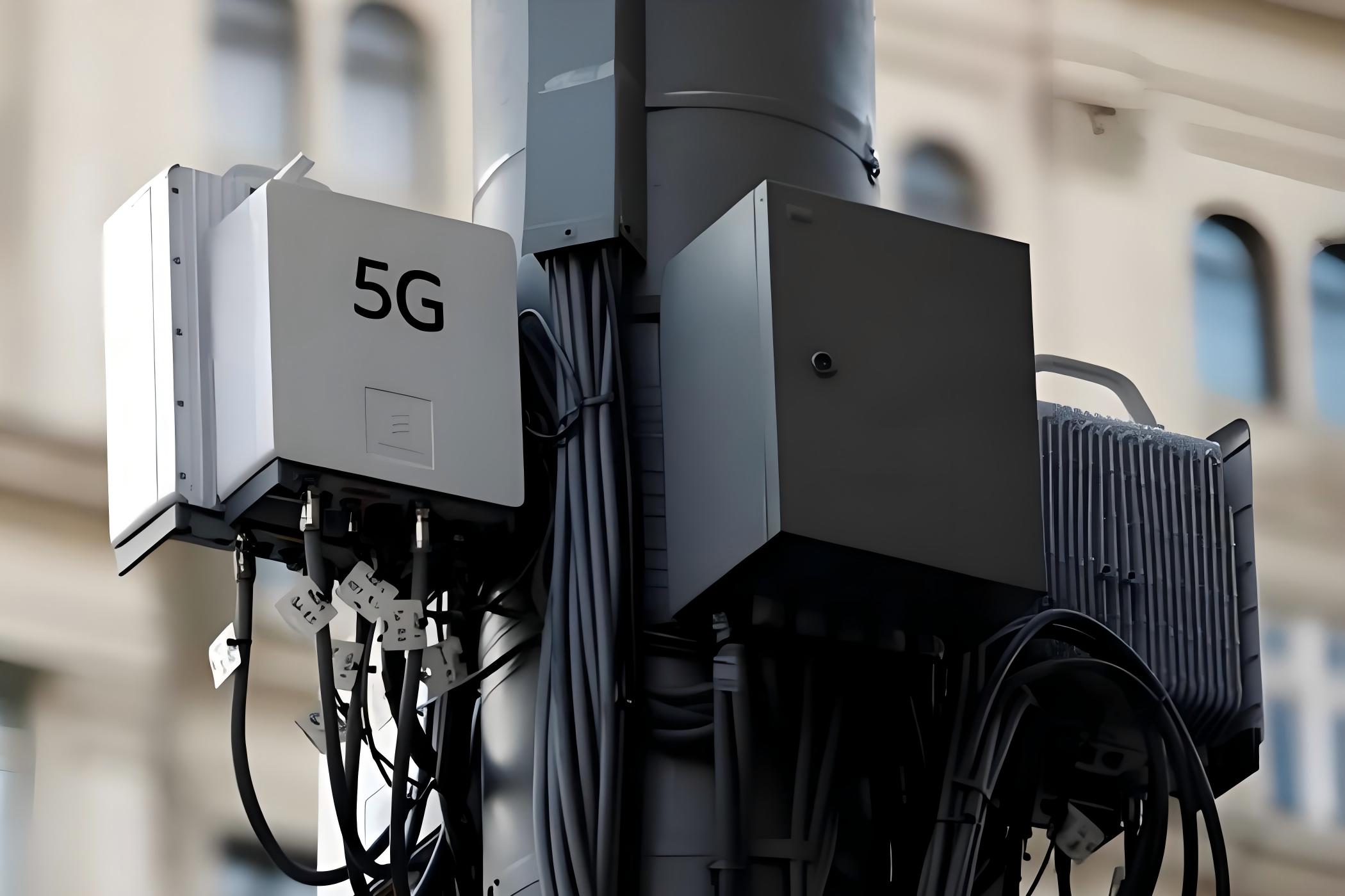
- High-Frequency Signal Integrity: Short-path routing + low-impedance copper layer reduces signal transmission delay by 40% and crosstalk by 50%. Ensures zero data loss in high-frequency interactions (5G/4G, NFC payment) and error-free transaction processing.
- Multi-Function Integration & Scalability: 8+ layer fine routing directly integrates processor, memory, biometrics, power management modules. Embedded capacitors/resistors cut external components by 30%. Reserved interfaces support AI algorithm/blockchain security module upgrades.
- Efficient Thermal Management: High-Tg substrate + thermal via/layer design doubles thermal conductivity, rapidly dissipates heat from chips/power modules. Reduces thermal stress risk by 50% for 24/7 operation, extending device lifespan by 20%.
- Cost-Benefit Optimization: Higher per-board cost offset by 15% reduction in overall materials (connectors, cables). Automated production (laser drilling, precision lamination) improves efficiency by 30%, shortens time-to-market by 20%, and lowers lifecycle cost by 10%.
- Future-Proof Tech Compatibility: Naturally compatible with 5G high-frequency RF circuits (low-loss microstrip transmission), AI chip high-density computing needs, and biometric module fine routing. Maintains device adaptability to rapid payment scenario evolution.
Applications of HDI Printed Circuit Board in Smart POS
- Integrate processor, communication module, security chip, touchscreen driver.
- Optimize 5G/4G, NFC, Wi-Fi high-frequency signal transmission.
- Integrate fingerprint recognition and facial recognition modules.
- Carry financial-grade security chip and encryption module.
- Dissipate heat from processor and power module.
- Integrate power management module and reduce power impedance.
- Reserve interfaces to support AI algorithms and blockchain module expansion.
- Each point directly maps to the core application scenarios of HDI PCB in smart POS devices, ensuring technical accuracy and concise expression.
Technical Parameter for Smart POS HDI Printed Circuit Boards
| Parameter | Specification |
| Substrate Material | High-frequency FR4 or polyimide materials; Tg value ≥170°C; Low dielectric constant (Dk ≤3.8) |
| Layer Count | 4-12 layer HDI structure with blind/buried via design |
| Line Width/Spacing | Minimum line width: 50μm; Minimum line spacing: 50μm |
| Drilling Specifications | Mechanical drilling: ≥0.15mm; Laser drilling: 0.05-0.1mm; Aspect ratio ≤10:1 |
| Surface Finish | ENIG (chemical nickel gold); Optional immersion silver/tin; Thickness: Nickel 3-5μm, gold 0.05-0.1μm |
| Impedance Control | Single-ended impedance: 50Ω±10%; Differential impedance: 90Ω±10% |
| Copper Thickness | Outer layer: 1/2oz-2oz (17-70μm); Inner layer: 1/3oz-1oz (12-35μm) |
| Solder Mask | LPI liquid photoimageable solder mask; Thickness: 15-25μm; Minimum opening: 75μm |
How HDI PCB Optimize High Frequency Signal Transmission Performance in Smart POS?
1. Precision Low-Loss Substrate Selection
- Material Specifications: Utilize high-frequency low-loss substrates such as Rogers RO4350B (Dk=3.48, Df=0.0021) and Panasonic MEGTRON 6 (Dk=3.7, Df=0.002), ensuring Dk ≤ 3.5 and Df ≤ 0.0025.
- Performance Enhancement: Achieves 70%+ reduction in 60GHz signal loss compared to FR-4, maintaining signal attenuation ≤2.5dB/cm for 5G/Wi-Fi 6/4G modules.
- Application Compatibility: Specifically designed to meet the high-frequency requirements of smart POS modules, ensuring robust anti-interference capabilities and stable communication links.
2. Stackup Structure Optimization
- Layer Configuration: Implement alternating “signal-ground-power” stackup (e.g., L1: Signal, L2: GND, L3: Power, L4: Signal) to minimize return path discontinuity.
- Noise Mitigation: Grid-like power plane design reduces power noise fluctuations to <50mV, while avoiding cross-split routing preserves signal integrity for DDR4/PCIe interfaces.
- Structural Advantage: Maintains unbroken reference planes under high-speed traces, critical for minimizing electromagnetic interference (EMI) and crosstalk.
3. Hierarchical Blind/Buried Via Application
- Via Type Selection: Deploy blind vias (1-2 layers) for fine-pitch BGA regions and buried vias (3-6 layers) for internal layer connections, optimizing routing density.
- Innovative Structure: The “1+2+1” blind via stack (top-layer blind via + internal buried via + bottom-layer blind via) increases routing density by >30% while reducing signal path length and transmission delay.
- Space Optimization: Minimizes through-hole space occupation, enabling compact layout design for high-density POS motherboards.
4. Precision Impedance Control & Matching
- Impedance Standards: Strictly control single-ended impedance to 50±10Ω and differential impedance to 100±3Ω via line width/spacing tuning (e.g., 0.1mm/0.1mm differential pairs).
- Verification Method: TDR (Time-Domain Reflectometry) simulations validate impedance continuity, ensuring 60GHz signal return loss ≤ -28dB to minimize reflection losses.
- Design Compliance: Adjusts dielectric thickness and copper weight to meet impedance targets, critical for maintaining signal integrity at high frequencies.
5. Differential Signal & Shielding Design
- Differential Pair Routing: High-speed signals (USB3.0/HDMI) are routed as differential pairs with length matching error <5mil to reduce common-mode noise.
- Shielding Implementation: Ground vias spaced <0.5mm alongside critical signal traces form electromagnetic shielding strips, suppressing crosstalk to <-70dB.
- Anti-Interference Enhancement: Creates a protective barrier against EMI, ensuring signal purity and reliability in dense POS environments.
6. EMI/Thermal Co-Design
- Electromagnetic Isolation: Ground planes segregate digital/analog domains with single-point grounding, while 0.01μF high-frequency decoupling capacitors suppress power noise.
- Thermal Management: Densely arranged thermal vias (0.3mm diameter, 1mm pitch) under power devices (e.g., LDOs/MOSFETs) form heat pathways to bottom-layer thermal pads, reducing single-via thermal resistance by 40%.
- Synergistic Effect: Prevents thermal concentration from degrading signal performance, ensuring system stability and longevity.
7. Simulation Verification & Process Control
- Simulation Tools: HyperLynx/Allegro perform time/frequency domain simulations to validate eye diagram margin (>20%), crosstalk (<5%), and impedance matching.
- Manufacturing Standards: Adheres to IPC-2221 specifications for minimum trace width/spacing (4mil/4mil), blind via diameter (≥0.1mm), and layer alignment tolerance (±50μm).
- Quality Assurance: X-ray drilling inspection ensures blind via positioning accuracy, boosting first-pass yield to >95% and ensuring design manufacturability and reliability for volume production.
How to Balance the Performance and Cost of HDI Printed Circuit Boards in Smart POS?
Layer and Structure Refinement Design
- Adopt symmetric stack-up structures from 1+N+1 to 3+N+3, achieve 0.1mm-level high-density wiring in the BGA region via laser microvia technology, and optimize signal path length.
- PWR/GND pins penetrate 1-2 layers via microvias, freeing up inner layer wiring space, reducing layer count by 20% compared to original design, and minimizing material usage.
- Wiring density increases by 40%, signal integrity improves by 12%, supports multi-layer any-layer interconnection design, and adapts to future functional expansion requirements.
- Optimize interlayer coupling capacitance, reduce crosstalk, enhance high-frequency signal transmission quality, and ensure stable 5G/NFC communication.
Material Grading Selection Strategy
- For high-frequency scenarios, select low Dk/Df materials (Dk ≤ 4.5, Df ≤ 0.005) such as PTFE substrate to reduce 5G signal loss by over 25%.
- For conventional scenarios, use high-Tg FR-4 (Tg ≥ 170℃) to balance cost and heat resistance, preventing substrate deformation under high temperatures.
- Hybrid outer-layer low-loss substrate with inner-layer conventional FR-4, achieving ≤5% performance loss, significant cost optimization, and suitability for mid-range POS devices.
- Select materials with low coefficient of thermal expansion (CTE) to reduce interlayer delamination risk caused by thermal stress and improve long-term reliability.
Manufacturing Process Adaptability Enhancement
- Implement mSAP/MSAP process to achieve 2mil/2mil line width, increasing wiring density by 30% and adapting to high-density wiring requirements.
- Control laser drilling precision to ±0.05mm, plating void ratio ≤3%, ensuring no short/open defects in microvias.
- Achieve 100% AOI inspection coverage, complemented by X-ray inspection, to identify interlayer alignment deviations and microvia filling quality.
- Optimize plating uniformity to avoid excessive copper thickness variation in microvia inner walls, preventing reliability issues and extending product lifespan.
Thermal and Heat Management Co-Design
- Metal substrate + buried copper block technology achieves thermal resistance ≤1.5℃/W, reducing processor area temperature by 20℃ and improving heat dissipation efficiency.
- Thermal via array density ≥20/cm², combined with thermal vias to form efficient heat conduction paths and reduce thermal hotspots.
- Embed liquid cooling microchannels between layers to reduce thermal stress risk by 50%, extend device lifespan by 20%, and support 24/7 high-load operation.
- Use high thermal conductivity (≥2W/m·K) thermal adhesive to enhance interfacial heat conduction efficiency and reduce thermal resistance.
Power and Signal Integrity Optimization
- Control PDN impedance ≤0.5Ω@100MHz and power noise ≤50mV to ensure power stability.
- Ground via spacing ≤0.2mm to form low-impedance return paths, reducing ground bounce noise impact on signals.
- Differential pairs adopt 4mil spacing + 50Ω impedance design, achieving ≥20dB crosstalk suppression and improving signal noise immunity.
- Optimize power plane partitioning to reduce power plane resonance, enhance power integrity, and support high-speed signal transmission.
Extensibility and Maintainability Design
- Reserve standardized interfaces (e.g., ZIF connectors) to support hot-swapping of AI algorithm modules and adapt to future functional upgrade requirements.
- Modular stack-up structure facilitates maintenance and component replacement, reducing total lifecycle cost by 15% and improving maintainability.
- Design DFT (Design for Testability) interfaces to support boundary scan and in-circuit testing, simplifying fault localization and repair processes.
- Adopt removable connector design to reduce on-site repair difficulty and time, improving device availability.
Why Choose EBest Circuit (Best Technology) as HDI Printed Circuit Board Supplier?
Reasons why choose us as HDI printed circuit board supplier:
- 19-Year Expertise for Risk Reduction: Leverage 19 years of HDI technology accumulation to provide expert consultation, reducing customer R&D trial costs by 30% and ensuring one-time certification approval for complex products like smart POS, minimizing rework expenses.
- Full-Inspection Quality Assurance: Implement 100% batch inspection + UL/IPC dual certification with defect rate ≤0.03%, directly safeguarding customer terminal products’ zero-fault rate, enhancing brand reputation, and reducing after-sales recall risks.
- 24-Hour Rapid Prototyping Service: Complete emergency order prototyping within 24 hours, accompanied by free DFM analysis reports to preemptively resolve 90% of potential production issues, accelerating product launch by 40% and securing market opportunities in emerging fields like 5G/mobile payments.
- Custom Material & Process Optimization: Select high-frequency low-loss substrates + ENIG surface treatment combined with laser microvia forming (≤100μm aperture) to boost signal transmission speed by 15% and reduce power consumption by 20% for smart POS, meeting high-speed payment scenario requirements.
- End-to-End Integrated Solutions: Cover full-process services from PCB design to SMT and PCBA assembly, reducing customer supply chain coordination efforts by 15%, expediting product commercialization, and supporting rapid iteration demands.
- Cost Optimization Guarantee: Offer 10%-15% lower custom quotes than industry averages through scaled production and material supply chain integration, while maintaining premium material usage to enhance customer profit margins and product competitiveness.
- Quick-Response Delivery Service: Ensure 7-day delivery for standard orders and 5-day expedited delivery for urgent orders, enabling customers to flexibly adapt to market fluctuations and avoid order loss or market share erosion due to delays.
- Multi-Scenario Reliability Validation: Conduct customized wide-temperature (-40°C~125°C) and humidity (95% RH) tests to ensure stable operation of smart POS in extreme environments, reducing customer return rates and after-sales costs by 30%.
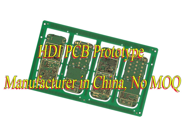
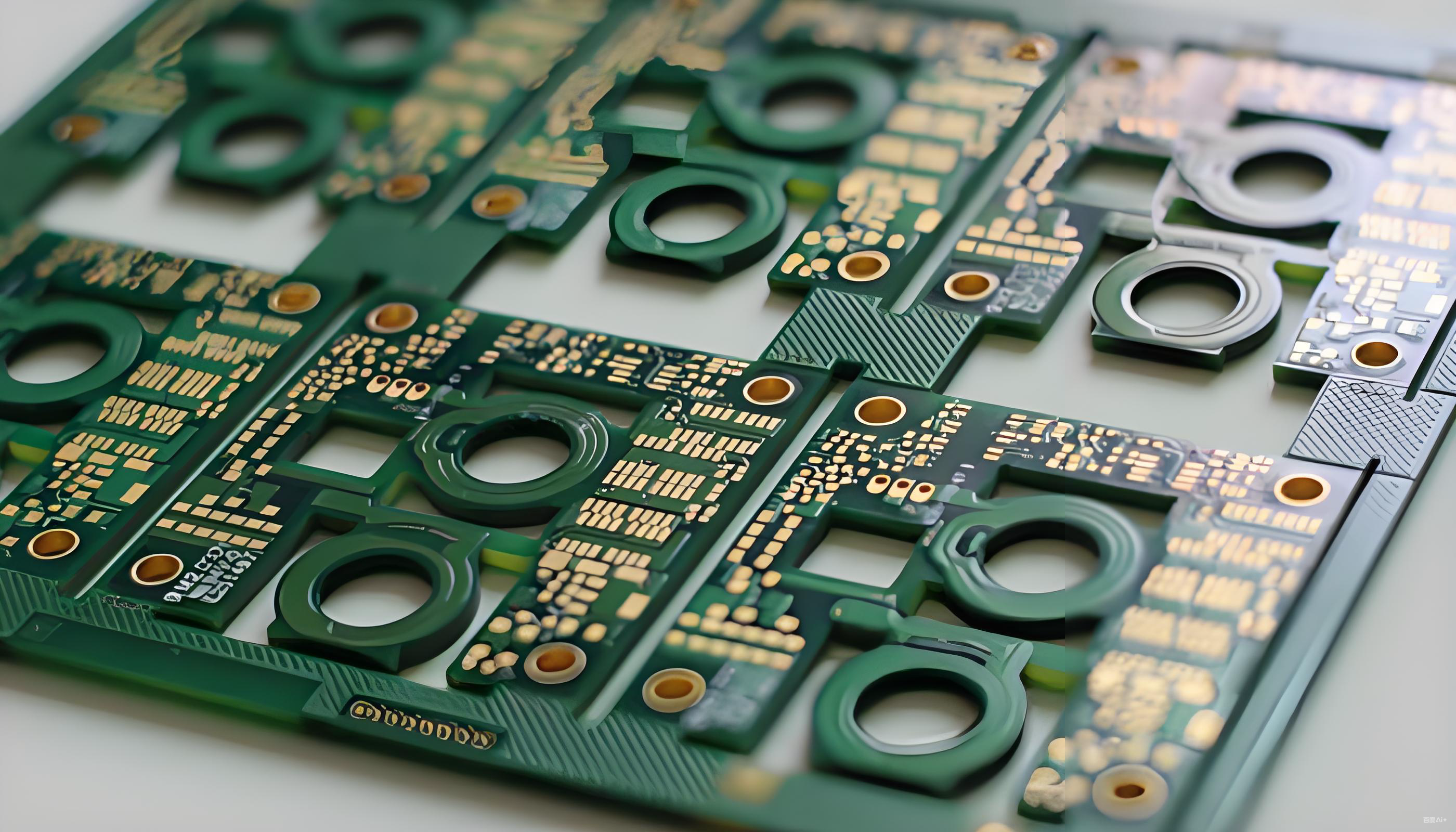
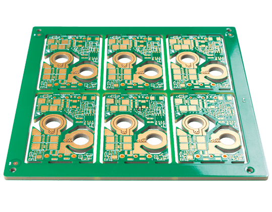
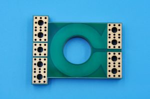
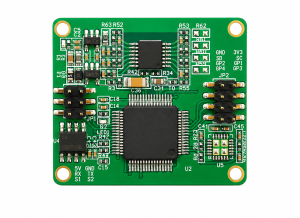
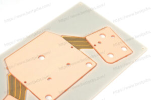
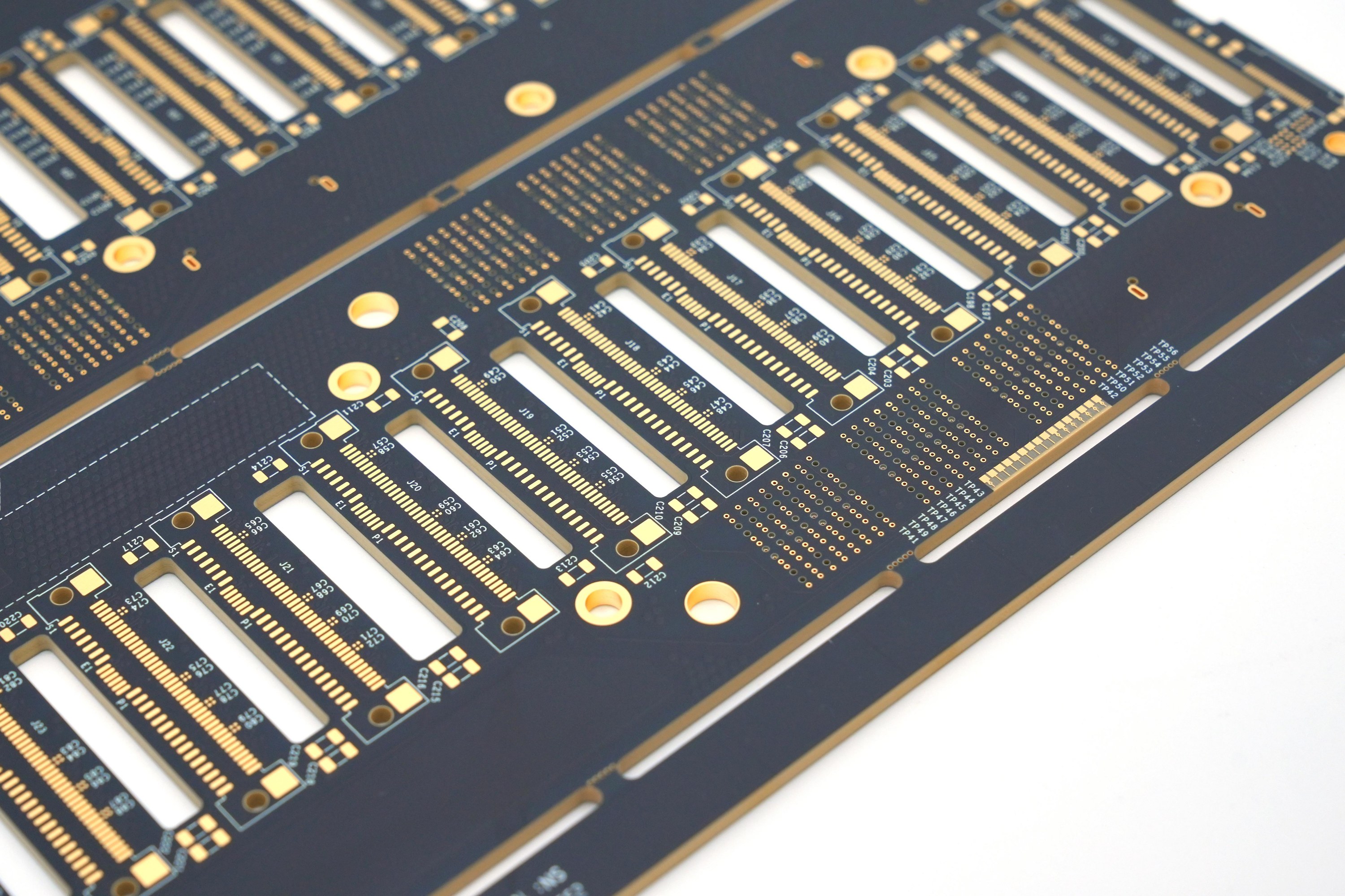
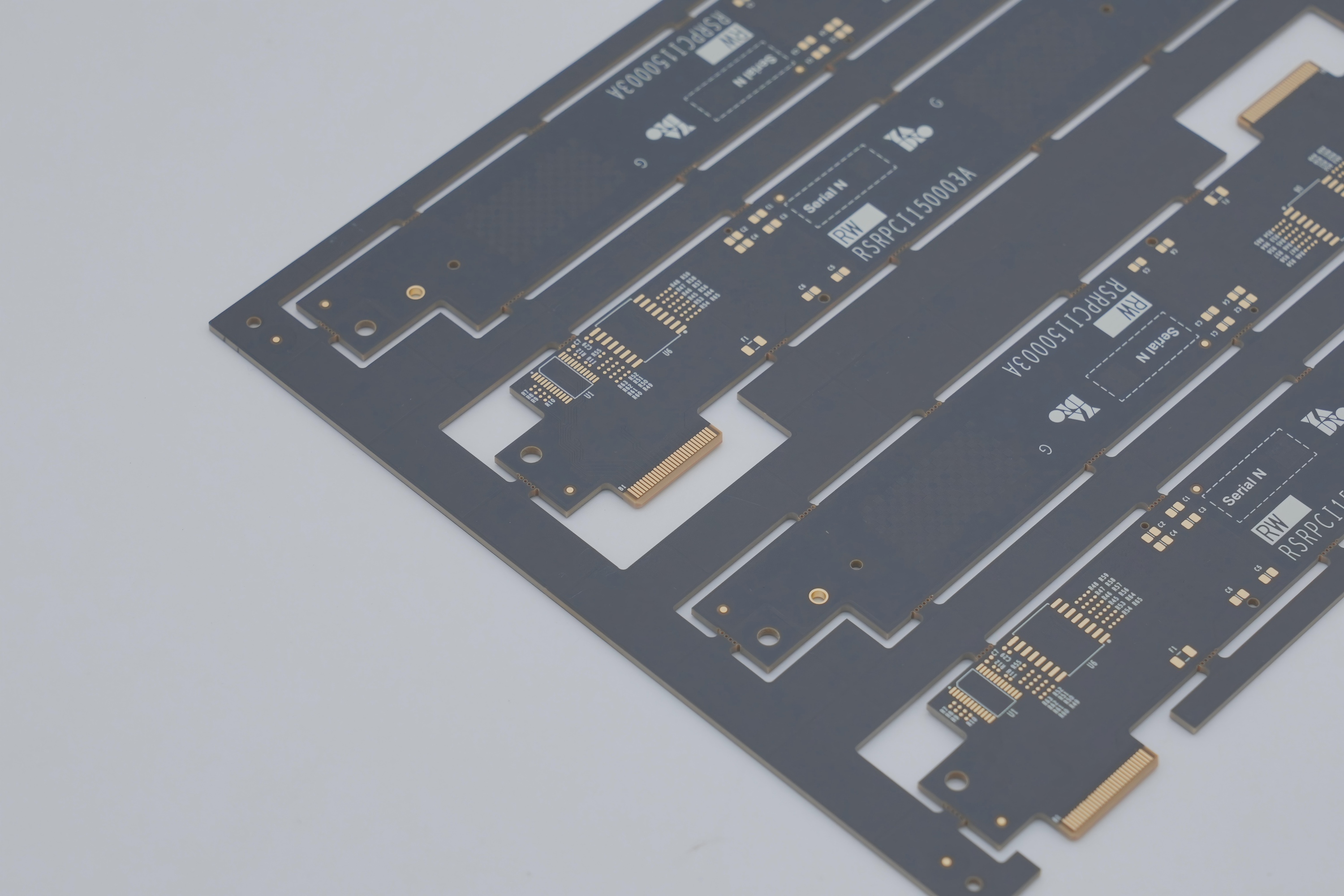
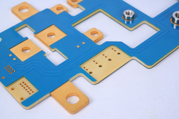
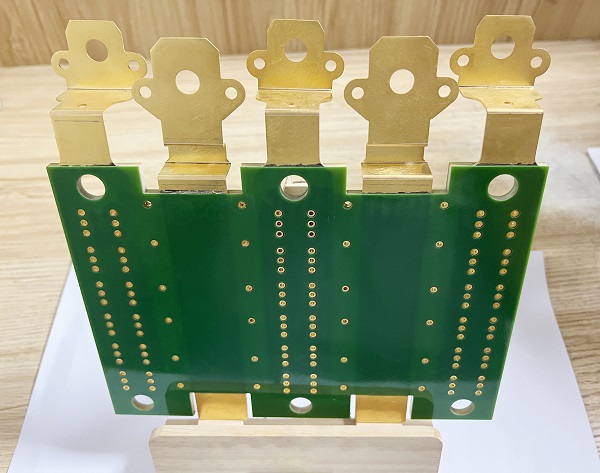
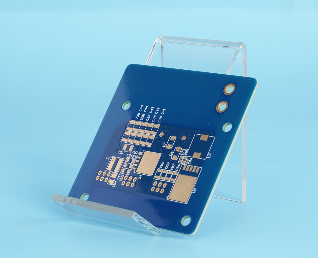
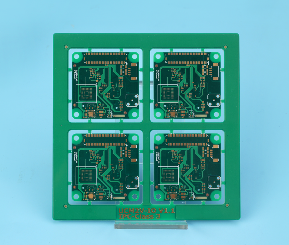
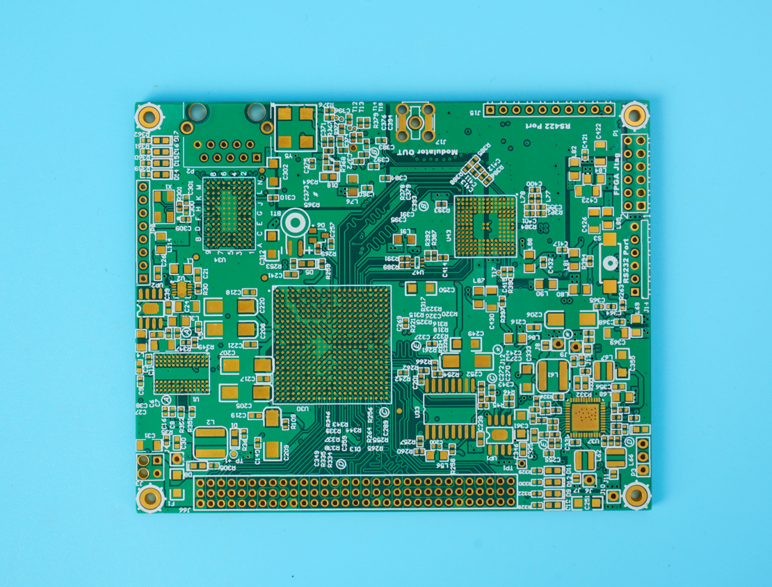
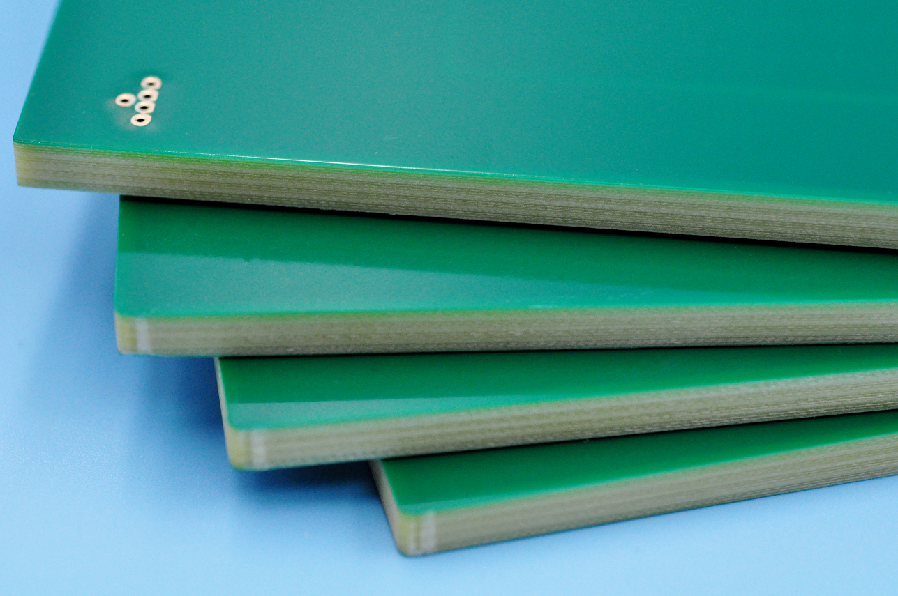
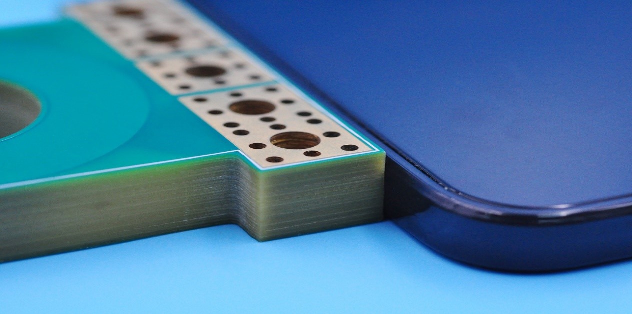
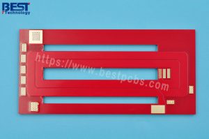
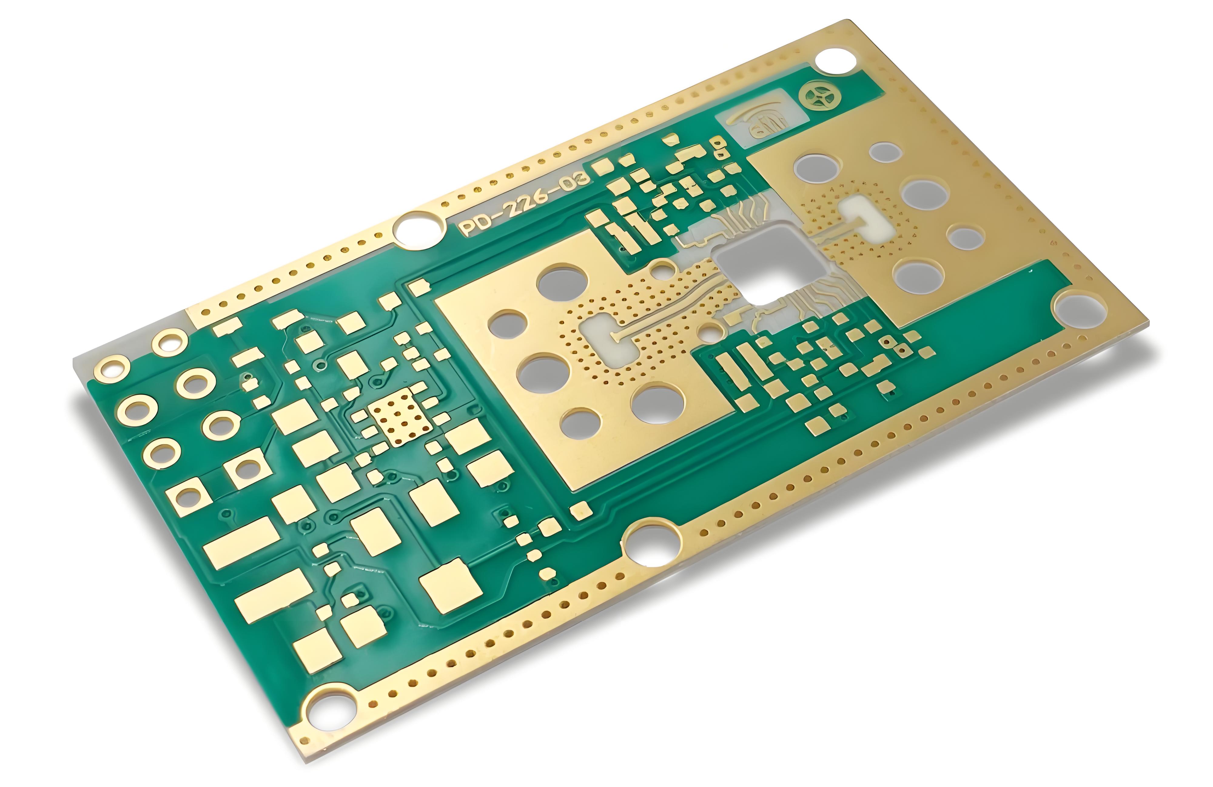
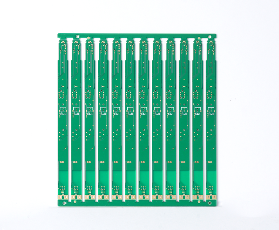
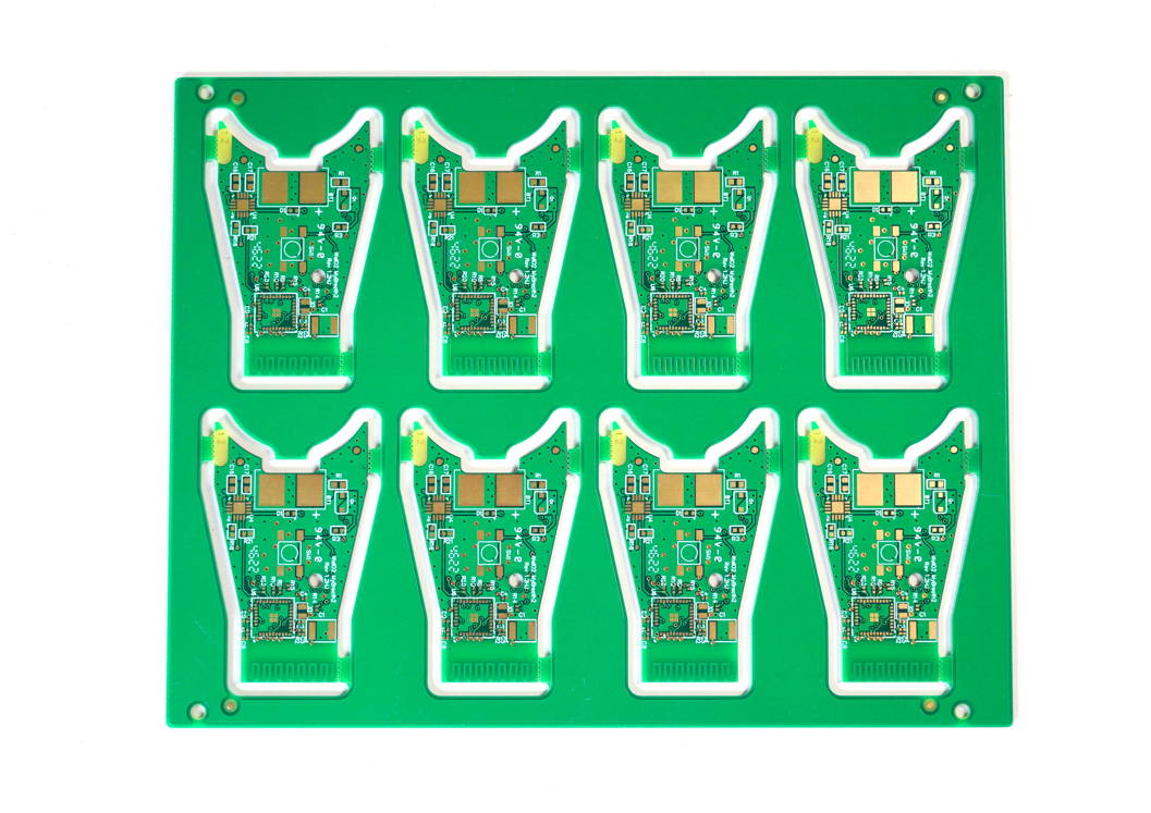
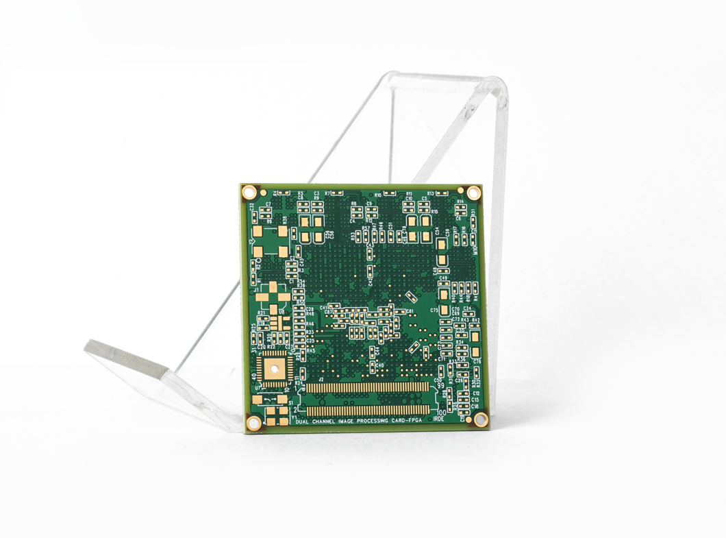
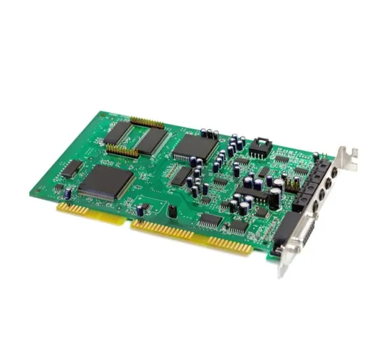
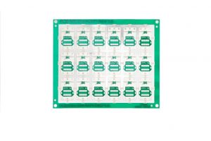
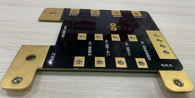
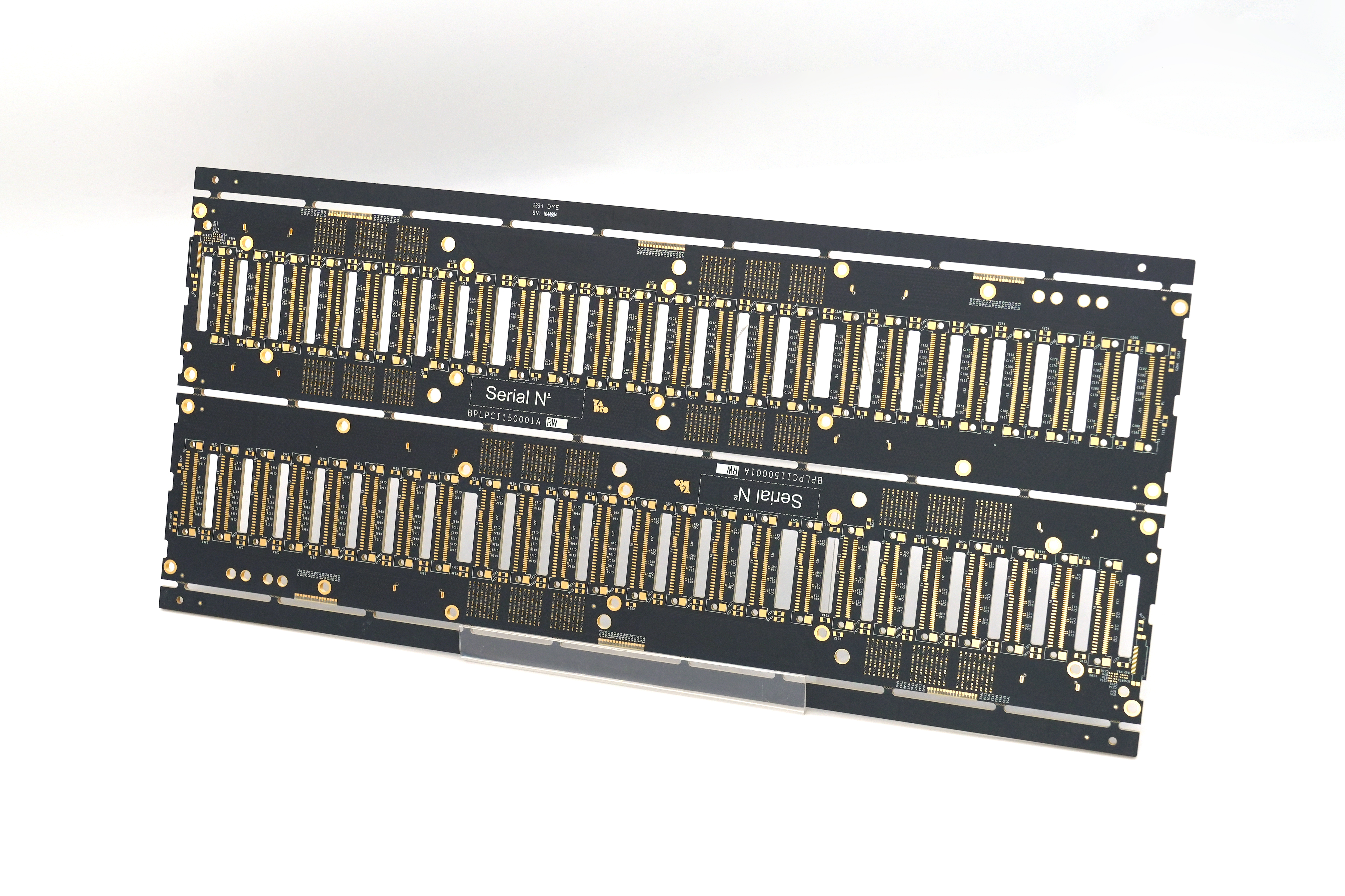
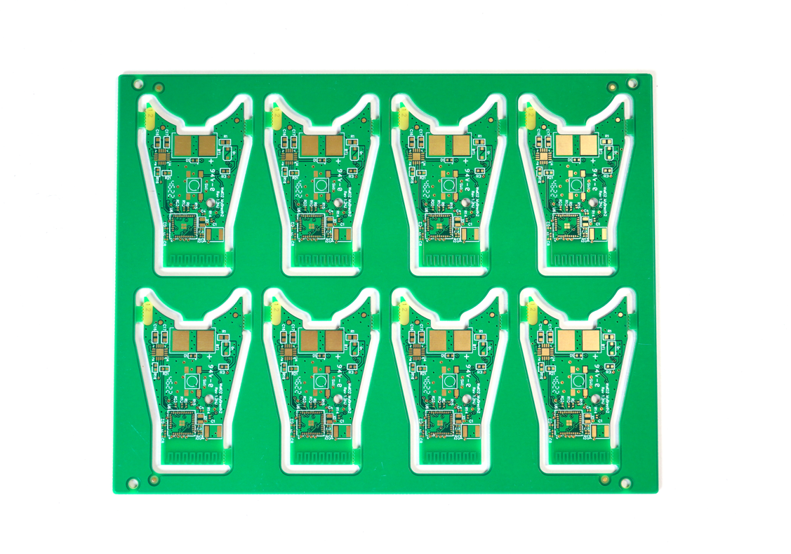
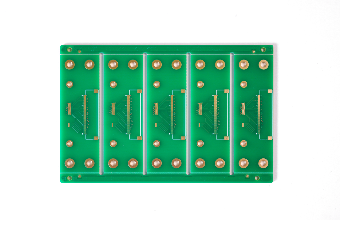
Below is a photo of HDI printed circuit board we did before:
Our HDI Printed Circuit Boards Capabilities
| Parameter | Capabilites |
| PCB Layers: | 1-32L |
| Copper Thickness: | Outer Layer:1oz~30oz; Inner Layer:0.5oz~30oz |
| Min Line Width/Line Space: | Normal: 4/4mil; HDI: 3/3mil |
| Min Hole Diameter: | Normal: 8mil; HDI: 4mil |
| PTH/NPTH Dia Tolerance: | PTH: ± 3mil; NPTH: ±2 mil |
| Surface Treatment: | ENIG(Au 4u’’),ENEPIG (Au 5u’’) Gold finger/Hard Gold Plating(Au 50u’’), HASL /LF HASL, OSP, Immersion Tin, Immersion Silver |
How to Get a Quote for Your HDI PCB Project?
The list of materials required for HDI PCB quotation is as follows:
- Layer count and stack-up configuration.
- Board dimensions and thickness.
- BGA region microvia specifications (0.1mm laser-drilled).
- Material grade selection (low Dk/Df PTFE or high-Tg FR-4).
- Copper weight and surface finish.
- Wiring density and signal integrity requirements.
- Thermal management specifications.
- Power integrity targets (PDN impedance ≤0.5Ω@100MHz).
- Manufacturing process control (mSAP/MSAP, ±0.05mm accuracy).
- Testing protocols (AOI/X-ray 100% coverage).
- Volume requirements and delivery timeline.
Welcome to contact us if you have any inquiry for HDI circuit board: sales@bestpcbs.com.