All works and no play makes Jack a doll. All the guys of EBest Circuit (Best Technology) have worked hard in 2018. In order to reward the members who worked really hard, we had a fantastic banquet on January 18, 2019.
At 7 PM, all the staffs attended the party and the party kicked off with the cheering and applaud. To begin with, our general manager Peter gave a speech which showed the conclusion of 2018 and his ambition for 2019.
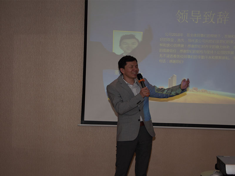
Peter gave a speech
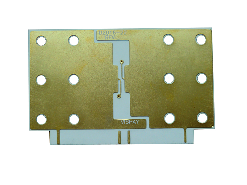
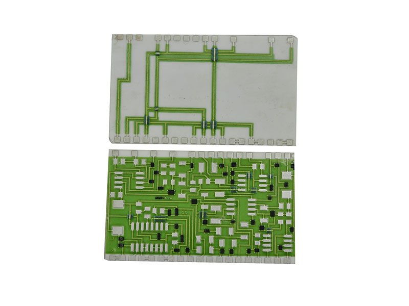
After the speech finished, we began to reward the staff one by one. Compared with the ceramic PCB, FR4 PCB and metal dome, the flex circuits got the first place. Mrs Celine won the sales champion of flexible PCB.
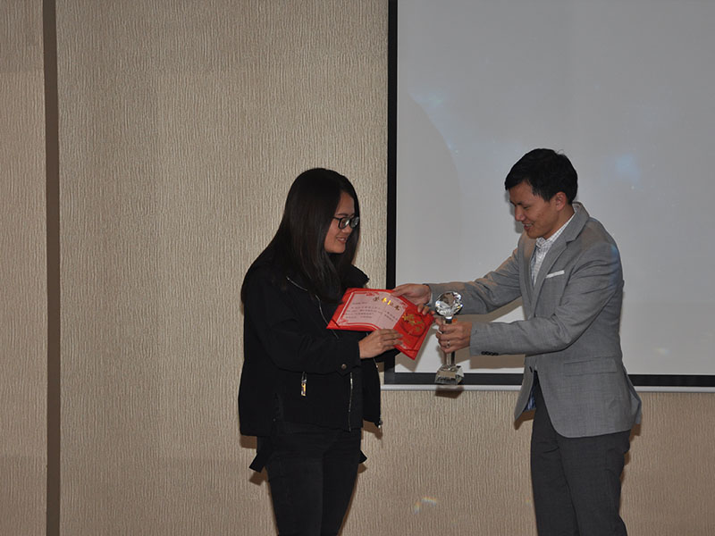
Celin won the champion of sales
Compared with last year, we have more entertainment programs in the banquet of 2018. Dancing, singing and games, all of these programs made us feel relax and forgot the pressure of work.
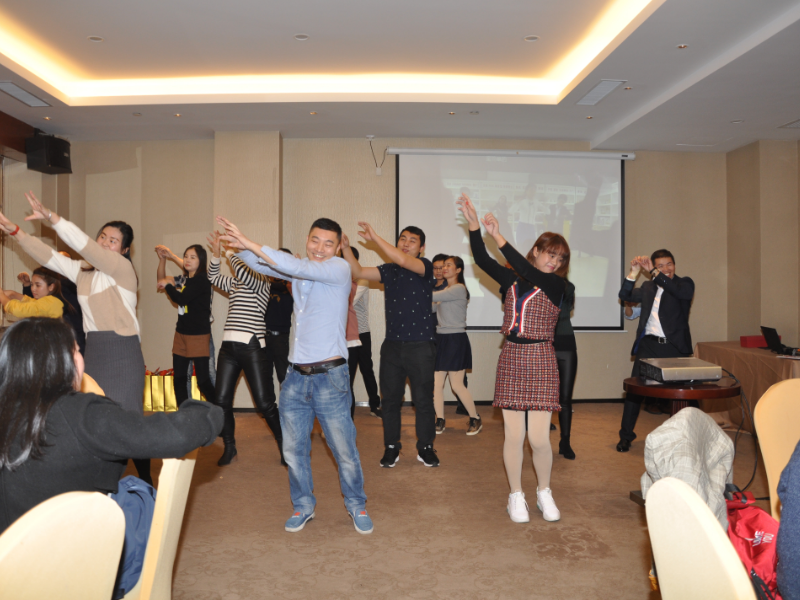
Dacing
What a fantastic banquet we had. Time flies, the beautiful night quickly came to an end and we took a family picture to remember this party.
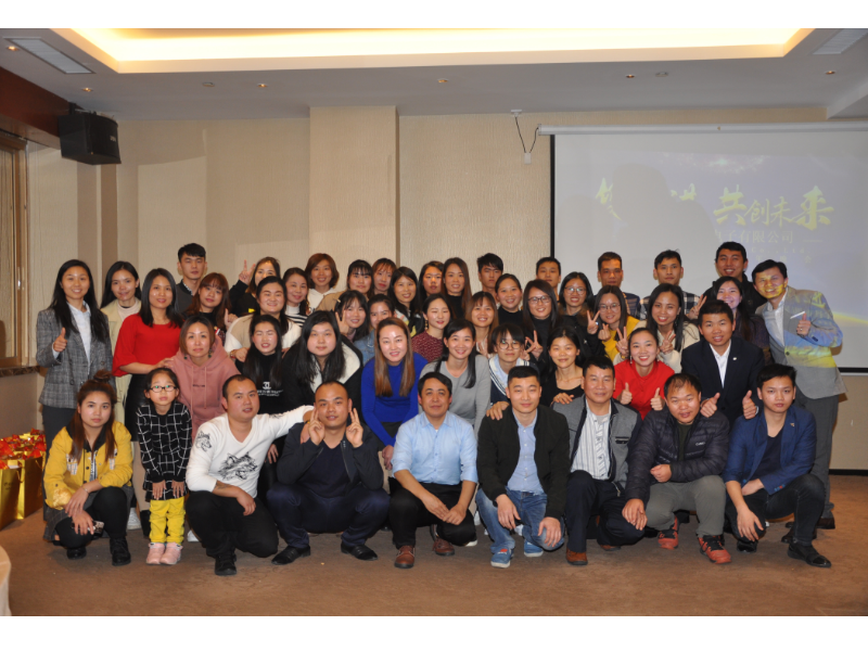
Family picture
2018 has gone, and we will hold hands and work together to achieve the gold of 2019. since throwing his hat into printed circuit board, EBest Circuit (Best Technology) is always dedicated to uphold our mission:to provide the most suitable products and the most satisfying service for our customers. If any interested in rigid PCB, rigid-flex PCB or ceramic PCB, please feel free to contact us at sales@bestpcbs.com or call us at 0755-29091601.