It is widely known that BeO with high thermal conductivity (200-250W/m.k).
High dielectric constant 6-7 (0.1MHz) and dielectric loss tangent is 10-4 (0.1GHz).
It is ideal material for ceramic PCB, lots of engineers want to use it as DBC ceramic PCB substrate.
But it is unfeasible, the powder of BeO is extremely poisonous.
The poison gas is produced by the reaction between oxygen, Cu and BeO under
1065-1085 degrees Celsius, so it is limited to make cooper on BeO substrate,
it has caused AlN (Aluminium Nitride) is becoming more and more popular.
Though BeO is unfeasible for DBC technology, but it is feasible for thick film technology.
Because when doing the conductor (Au or AgPd) on BeO substrate, we use silk-screen printing, no need to under high temperature environment, there is no chemical reactions.
Below the manufacturing process for your reference.
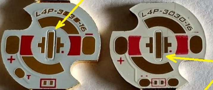
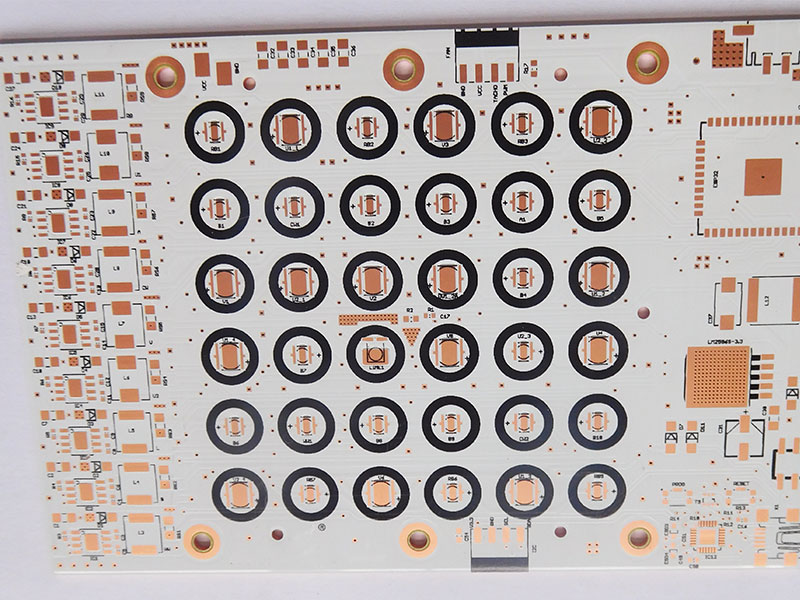
we can know that the high power LED’s thermal pad can touch the convexity area of copper core directly, so the heat of LED will be dissipated into the air much faster and more efficient than conventional MCPCB, but if only the LED pad can be designed as SinkPAD?
Actually the pads of other chips or components also can be designed as SinkPAD, one of the most common is the IC pad. In some designs, IC needs to pass through the large current, so it will emit a lot of heat.
In order to dissipate heat in time, some customers will directly design the IC solder pad as sinkpad to directly contact the copper base, so that the life cycle will be longer.
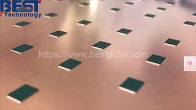
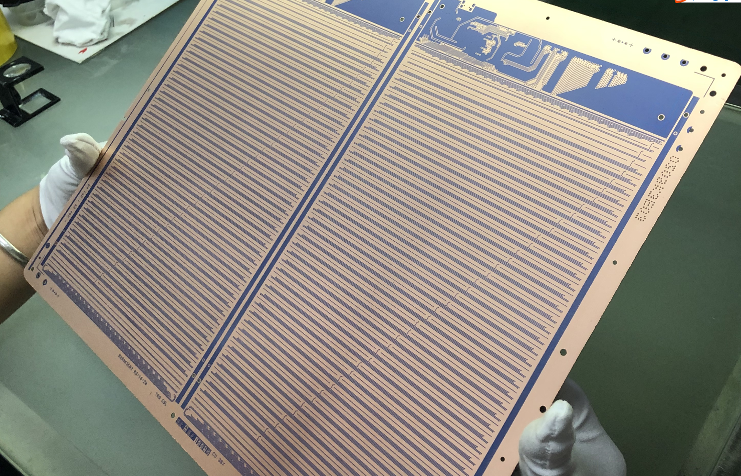
As you can see the following picture, it’s the copper layer after doing Etching, the area with blue film we normally named it as convexity, the thermal pad of IC will touch the convexity directly to achieve the purpose of dissipating the heat very fast.
If you have other questions about SinkPAD, welcome to contact Tammy (Email:sales9@www.bestpcbs.com), she will prove you professional suggestions and solutions.
Everyone may know that PCBs are easy to be bended or warped when get through the reflow process. Do you how to avoid this issue? here are some advices your reference.
Reduce the effect of temperature on PCB board stress
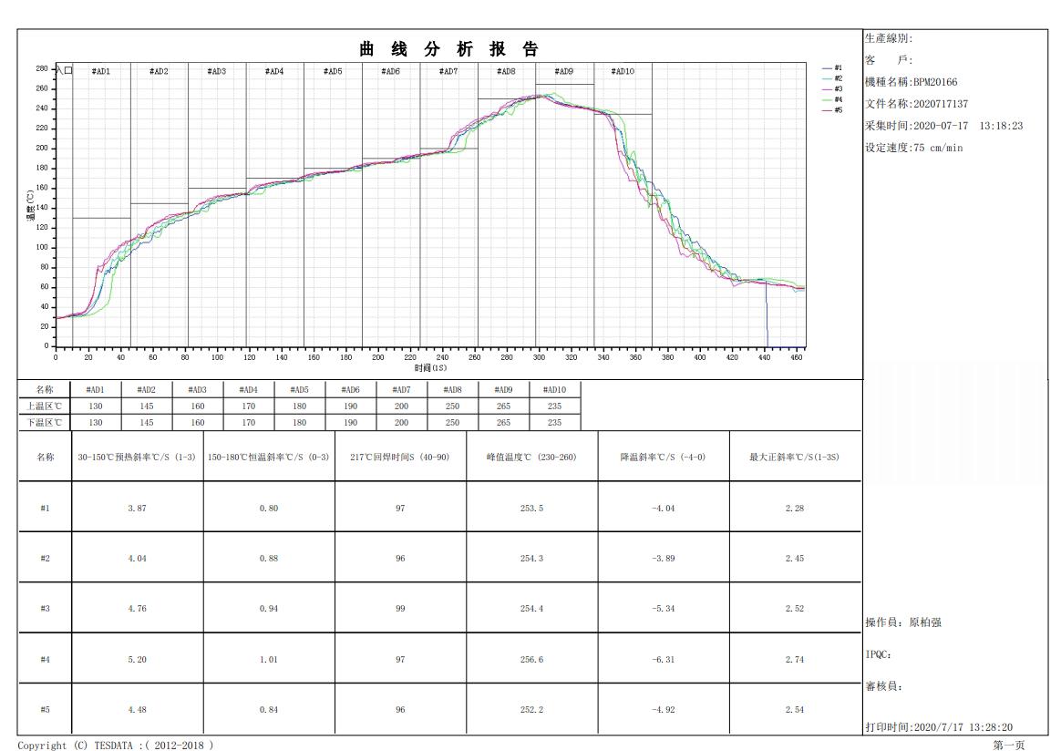
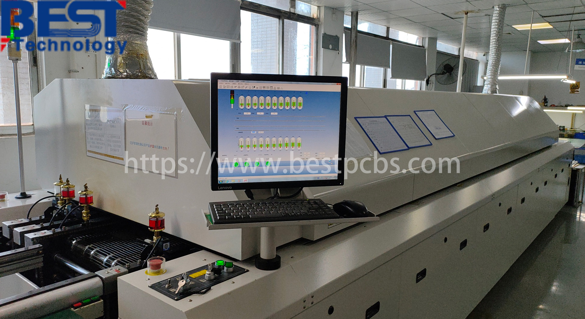
Due to the “temperature” is the main source of stress for board, so as long as the temperature of the reflow oven reduce the temperature or slow the speed of warming up and cooling down in the reflow oven, the board bending and warping issue can be reduced. But it may be occurring other issues, such as short circuit when soldering. See Best Tech make control for the temperature of the reflowing process.
reflow machine
2. Use high Tg plate
Tg is the glass transition temperature. The lower of the Tg value, the faster of board starts to soften after finishing reflowing, and deformed of the board become more serious. if use of higher Tg 170 material can increase the ability to withstand stress deformation, but the price of TG170 material is higher. See the stock of high Tg material from Best Tech.
Use high Tg plate
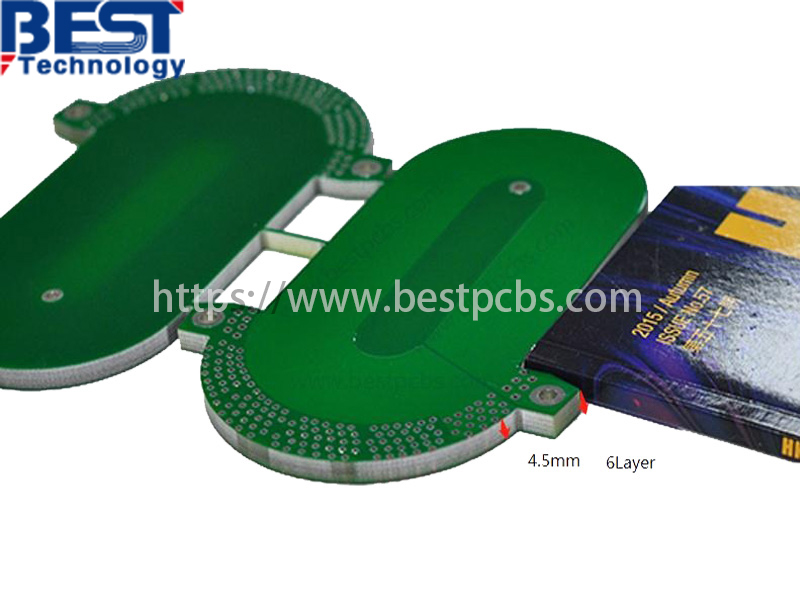
3. Increase the board thickness
If final application allowed, we recommend 1.6mm thickness to prevent the risk of board bending. Best Tech can provide PCB board thickness to 4.5~8.0mm.
PCB board thickness
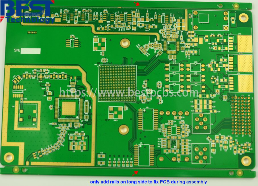
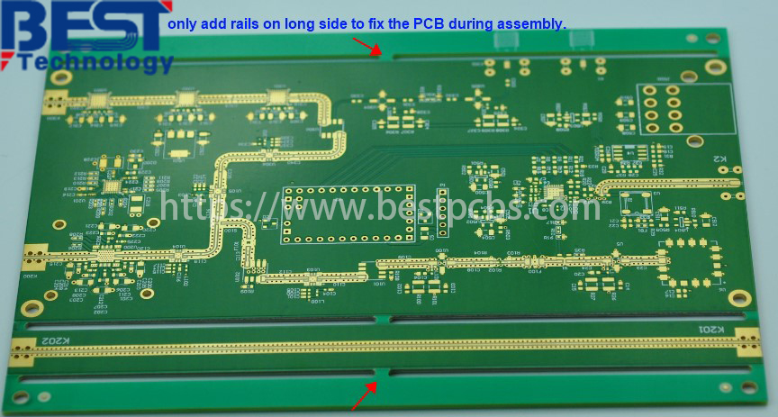
Try to reduce the size of the board and the number of panels during design
Since most reflow oven use chains to driving the board forward, if larger size of the FR4 PCB, the own weight will be deformed in the reflow oven, so during design try to design the long side of the PCB as a board edge, it can reduce the deformed. And
Same reason, if there are many PCBs in a big panel, PCB will be bigger and heavier, when get through the oven, the speed in the oven will be slowly and it will influence the deformed of the PCB. See following PCB board, we only panel 1 single piece into a panel to keep the size of FR4 PCB panel not bigger.
pcb
pcb
5. Use the reflow carrier/tray
If above methods cannot get a good result for deforming, you maybe can use a reflow carrier/tray to reduce the deformation. The reason reflow tray can fix the circuit board, after the temperature of the printed circuit board is lower than the Tg value, it can maintain the original size.
pcb in tray
6. Use Router instead of V-Cut
Since V-Cut will destroy the structural strength of the panels, try to use Router PCB board or just reduce the depth of the V-Cut will helps the deform issue.
pcb
pcb
If you want to know more about how we control the bended and warped for PCB, you are welcome to contact us.
Very few people know that there is AMB (Active Metal Bonding) ceramic PCB.
Do you know what’s the advantage for AMB ceramic PCB compare with other ceramic PCB (Al2O3/AlN/BeO/Si3N4 PCB)?
For AMB PCB, the substrate can be AlN ( Aluminium Nitride) and Si3N4 (Silicon Nitride) normally, AlN is the most popular. It is widely known that AlN with very high thermal conductivity ( Theoretical Value is 320W/m.k).
Using AMB technology to combine the oxygen-free copper and AlN material under high temperature, AlN with smaller thermal resistance, lower coefficient of thermal expansion and more stable partial discharge capability.
Compared with the traditional DBC or other substrate, the Aluminum Nitride copper-clad ceramic substrate made by the AMB technology with higher bonding strength of the copper layer and better cold and hot cycling characteristics.
So it is widely used in the field of IGBT, especially for the high-power device control module.
AMB with competitive price and the copper thickness can be much thicker.
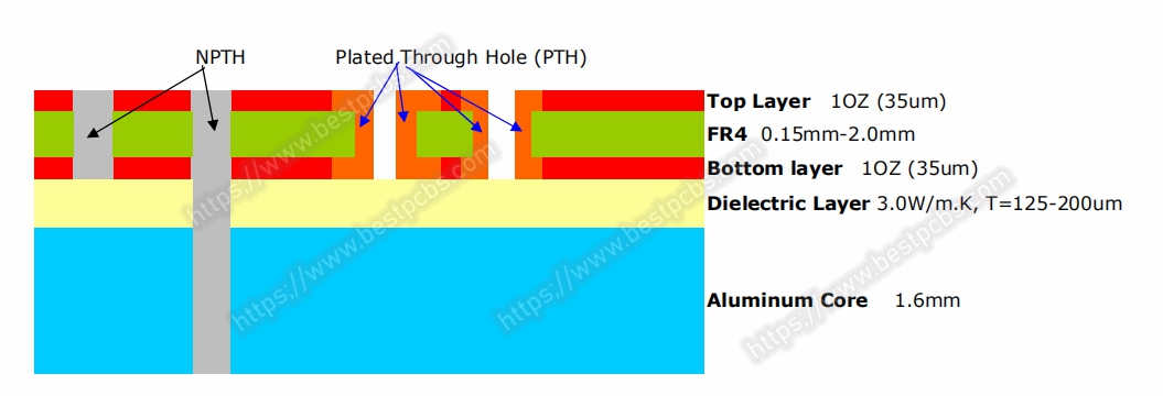
Metal Core PCB are differentiated on the basis of their construction, which can be divided into following types: single layer, double/two layers, double sided, and multi layer. The double sided and double/two layers MCPCB are commonly used in advanced electronic circuits, some people may be confused about them due to their similar names. So in this blog I’d like to share with you the differences between the two types.
Actually the main difference is the double sided and double/two layers MCPCB have different layout due to the positioning of the metal core.
Double/two layers MCPCB
As you can see the following stack up, the metal core is at the bottom, with two copper layers on top side, the dielectric layer is between the copper layer and the bottom metal base. In short, the conductor layers is in same side of the metal core. The components can only be assembled on the top layer.
double/two mcpcb stack up
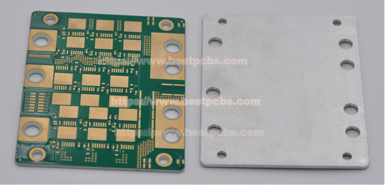
double/two mcpcb
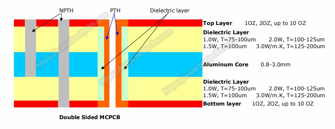
Double sidedMCPCB
As you can see the following MCPCB stack up, the metal core is in the middle of two conductor layers. There is also a dielectric layer between the metal core and a copper layer. The metal core and conductors are connected to each other through PTH (Plated Through Hole). The components can be assembled on both the bottom and top.
double sided mcpcb stack up
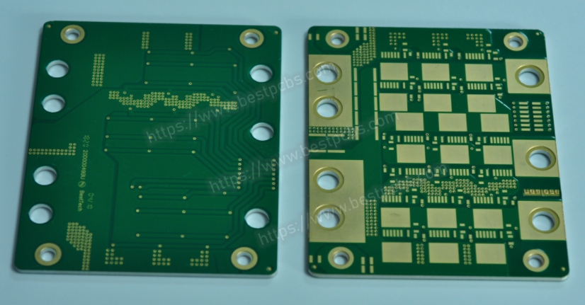
double sided mcpcb
Double sided MCPCB
Both double sided and double/two layers aluminum/copper core have the good heat dissipation, reliable performance at high temperatures and excellent thermal expansibility, according to our experience, for the same design, the heat dissipation on Double Sided MCPCB is a little better than Double Layers MCPCB.
The choice of the either type will depend on customer’s application requirements. If you are still confused about the two types and their benefits for your application, please feel free to contact Tammy (Email:sales9@www.bestpcbs.com), the Metal Core PCB International Sales in EBest Circuit (Best Technology).
Welcome to visit our website to learn more about us, we can provide different types of MCPCB in diverse specifications.
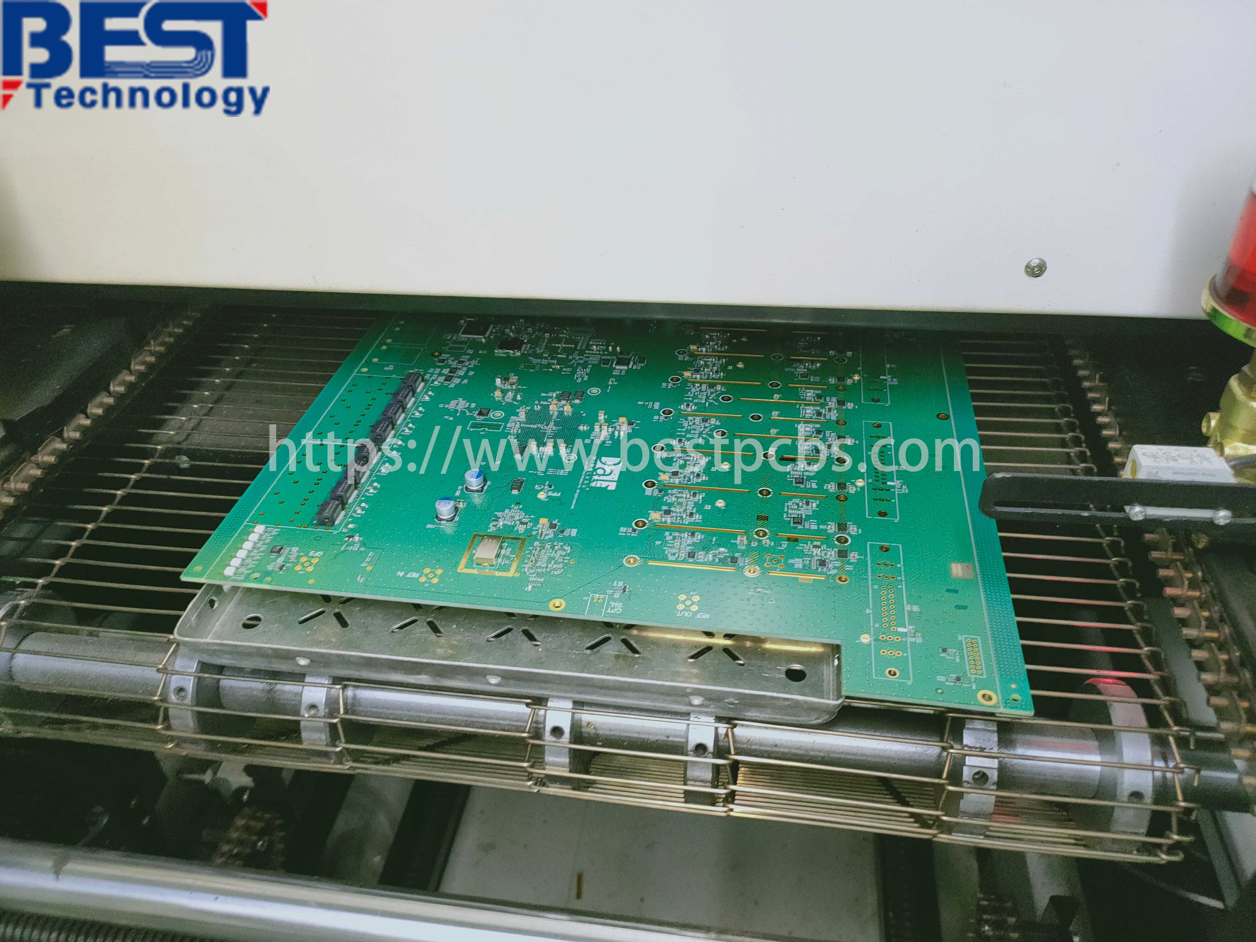
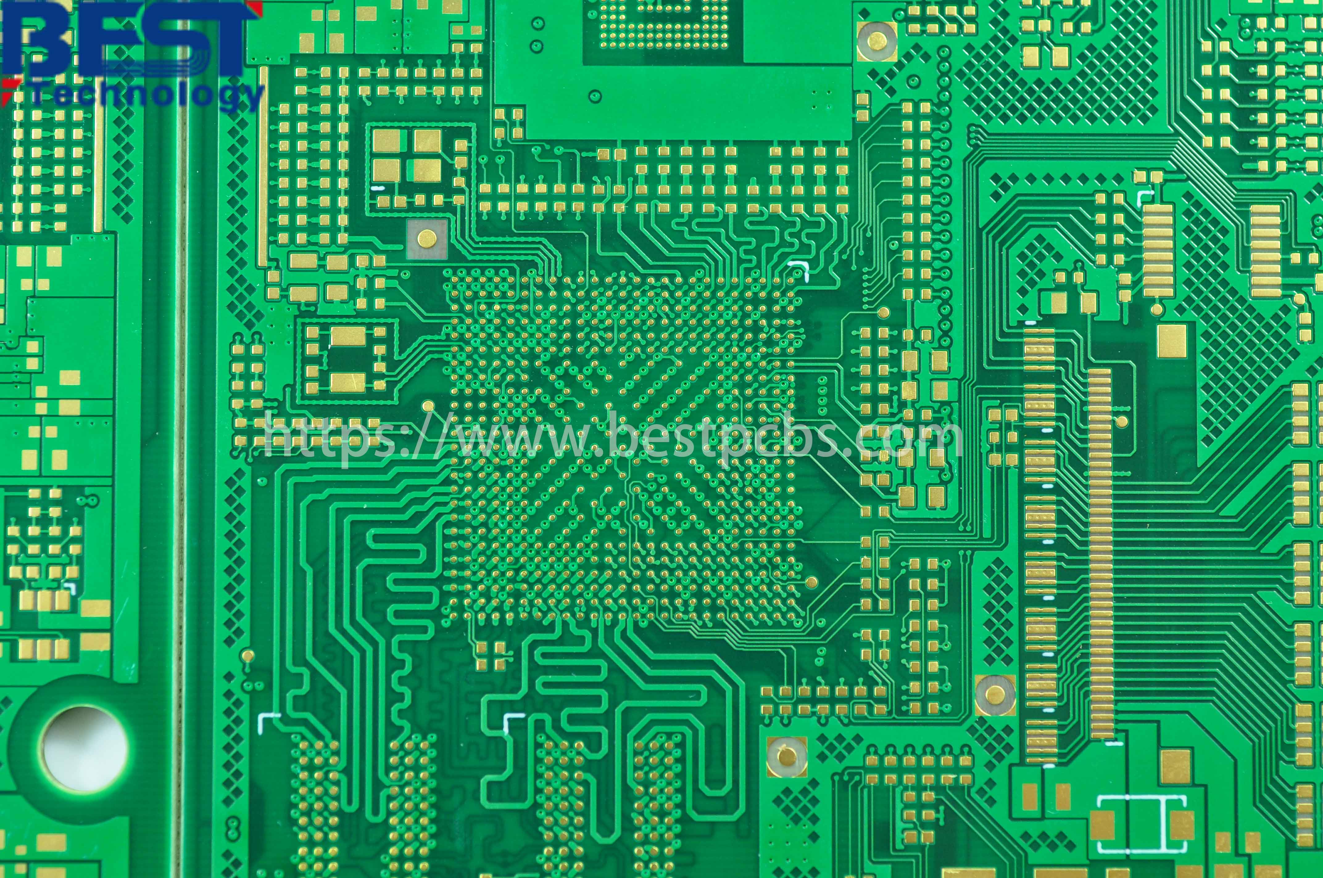
As we all know, the short & open circuits is a very common issues for the Printed Circuits Board, especially for the extra thin PCB, because its substrates thickness are very thin, generally from 0.4mm-0.15mm, so the circuits will be easy to be broken if we didn’t control the production process well.
So, you may want to know, as an experienced PCB manufacturer, what we will do to avoid the circuits issues?
Here let me show you what we do:
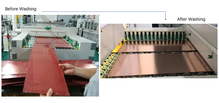
Firstly, after the process of copper plating, we will put the boards into our washing line to remove those drilling burr, surface oxide layer, etc. To make sure the boards are fully clean before start the traces making process.
pcb washing
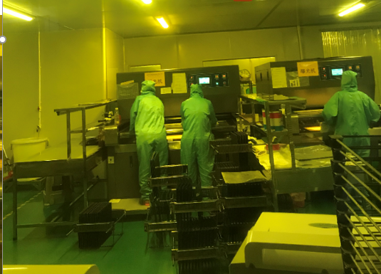
Actually, most of the open and short circuits problem are caused by the film scratching, so each operation while the pattern transfer process is very important.
That’s also why the exposure and developing need to be processed in the dust-free workshop. We will use the rack to place each PCB board separately, to avoid the touching between PCB.
pcb explosure and developing
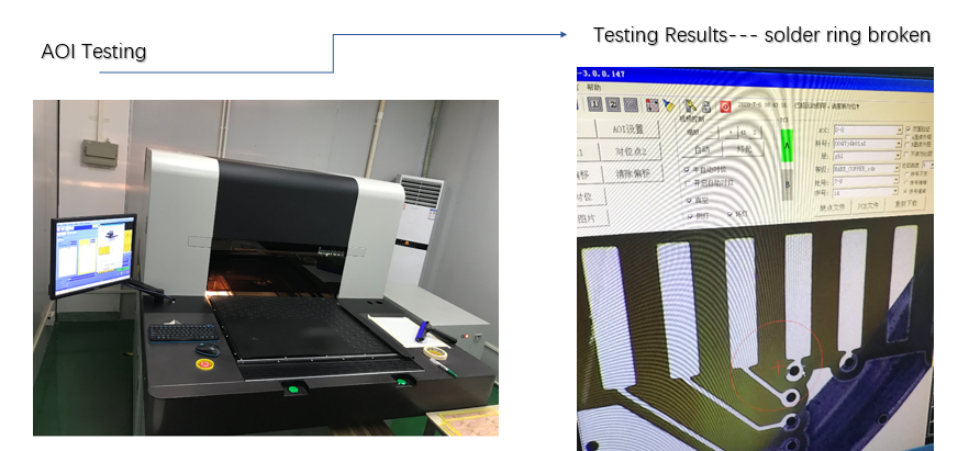
After the circuits etching out, we will take the boards to do the AOI testing, to check if there are any broken circuits, short gaps, protrusions, copper surface garbage and other problems. If there is, our machine will alert the problem, and we will fix the problem or scrap the defectives boards, with this process to prevent the defective boards move to the next step.
Most importantly is that we will do the first article inspection for all the boards, as long as we found the circuits issues while the AOI process, we will not take the whole batch boards go ahead.
aoi testing
Besides, the operation standard while the etching process is also very important for how the traces being. So, our production team will control the running speed of the etching machine very strictly. If it is a PCB with o.5oz bottom copper , only allow walk 1.4 meters at per minute, if 2oz, walk 0.8m one minute.
etching pcb
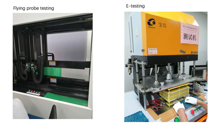
Except above process, all the boards will be required to do a final electrical testing before move to the packing. For prototypes, we will use flying probe testing. For volume, we will open the E-testing fixture to do the testing.
In our company, for the extra thin PCB, if the boards thickness lower than 0.2mm to do the flying probe testing, it needs to be tested before the outline process, because the boards are too thin to support the boards well while the flying probe, it will fall down easily.
flying probe testing and electric testing
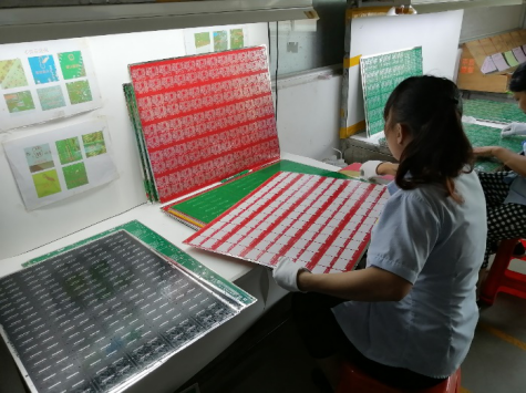
Of course, our QC people will do the double visual inspection to make sure all the boards are being well made.
fr4 pcb inspection
We always try our best effort to prevent any defective boards send to customers.
Quality and Customers Scarification, it is always our company’s pursuit.
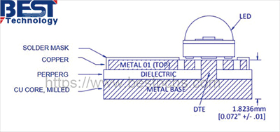
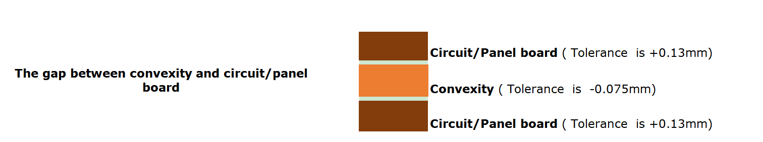
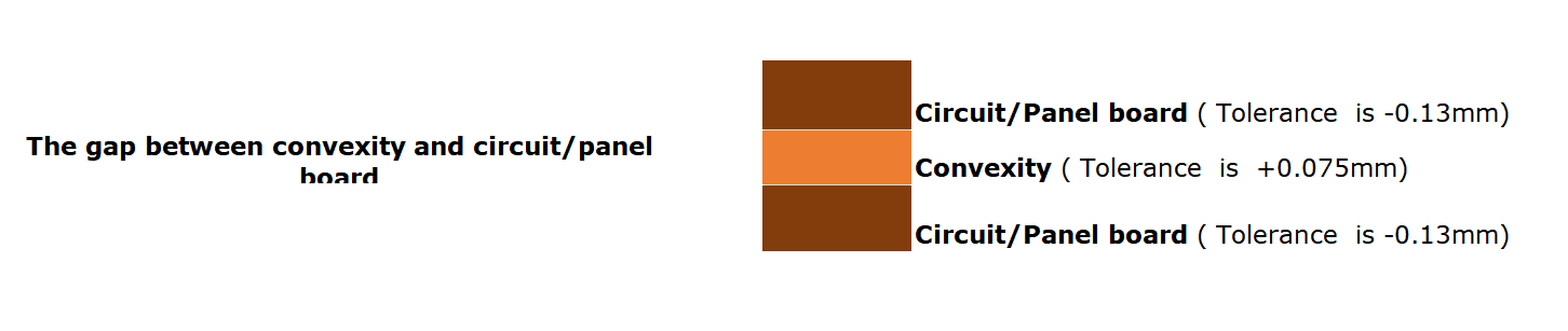
About the SinkPad copper core PCB, all is known that convexity is very important, the height of convexity is about 0.2mm-0.25mm.
We need to know what’s the reasons caused the gap between the convexity and LED pad is big.
We make the copper core with convexity firstly, then make the circuit/panel board (FR4PCB/BT PCB) and finally do the lamination for cooper core and circuit board.
The tolerance for convexity is +/-0.05mm-0.075mm.
The tolerance for circuit/panel board is +/-0.13mm.
If we do negative tolerance for convexity and positive tolerance for circuit/panel board, then it will cause the gap very big.
See below picture and details.
For example, the size of convexity is 0.5mm, after negative tolerance -0.075mm, it will be 0.425mm and each side will be 0.0375mm smaller.
For the circuit/panel board, the gap between convexity is 0.2mm, after positive tolerance +0.13mm, it will be 0.33mm and each side will be 0.065mm bigger.
So finally, the gap will be 0.2mm+0.0375+0.065mm=0.3025mm. It is about 50% bigger than original size.
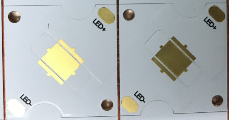
sinkpad pcbBig gap between convexity and LED pad
How to improve that problem?
Making the copper core with convexity according to design.
Measuring the dimension of convexity before making the circuit/panel board, then making the circuit/panel board according to the convexity dimension with compensation design.
Do Positive tolerance for convexity and negative tolerance for circuit/panel board, the gap will be much more smaller.
For example, the size of convexity is 0.5mm, after negative tolerance +0.075mm, it will be 0.575mm and each side will be 0.0375mm bigger
For the circuit/panel board, the gap between convexity is 0.2mm, after positive tolerance -0.13mm, it will be 0.07mm and each side will be 0.065mm smaller.
So finally, the gap will be 0.2mm-0.0375-0.065mm=0.0975mm. It is about 50% smaller than original size.
dtp pcbGood gap between convexity and LED pad
For more information about SinkPad PCB, please click
In high-speed PCB design, the seemingly simple vias often bring great negative effects to the circuit design. In order to reduce the adverse effects caused by the parasitic effects of vias, in the design, you can do as much as possible:
High-Speed PCB Design Principles
1. From the two aspects of cost and signal quality, choose a reasonable size of via size. If necessary, you can consider using different sizes of vias. For example, for power or ground vias, you can consider using larger sizes to reduce impedance. For signal traces, you can use smaller vias. Of course, as the via size decreases, the corresponding cost will increase.
2. The two formulas discussed above can be concluded that the use of thinner PCB boards is beneficial to reducing the two parasitic parameters of vias.
3. The signal traces on the PCB board should not change layers as much as possible, that is to say, try not to use unnecessary vias.
4. The power and ground pins should be drilled through the hole. The shorter the lead between the hole and the pin, the better. You can consider making multiple vias in parallel to reduce the equivalent inductance.
5. Place some grounded vias near the vias for signal changeover to provide the closest loop for the signal. You can even place some extra ground vias on the PCB.
6. For high-density high-speed PCB boards, consider using micro vias.
If you have any questions, or suggestions, welcome to leave your comments.
SinkPad PCB is a type of Copper base PCB used in thermoelectric separation application. It generally used for high power LED, the pad of LED touch the copper base directly, so that the heat generated by LED will dissipate quickly, which can achieve the best heat dissipation and conduction.
sinkpad gerber
sinkpad pcb
In another words, it is a technology that require to increase the path of the LED pad to the copper base to accelerate the heat emission from the base material. The copper base is vital while it also cost higher.
Then in order to lower cost, can SinkPad PCB use aluminum base instead copper base for heat dissipation?
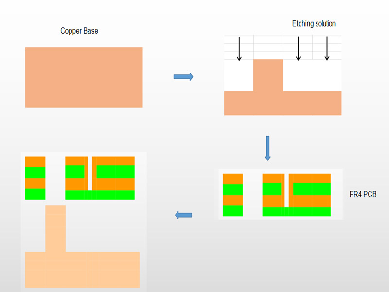
The answer is NO. As you can see the below manufacturing steps, the SinkPad will etch the copper base into convex platform with Copper Etching Solution, then hollow out the Double Layer FR4 PCB, and do lamination with the convex platform.
sinkpad pcb manufacturing steps
However, regarding of current technical conditions, since aluminum or aluminum alloy cannot directly react with acid, the reaction process is too complex and difficult to control, which will increase the difficulty of etching the LED pad platform. Considering the scrap rate, the process of etching LED pad platform with aluminum is more complex and the overall cost is higher.
It is widely known that BeO with high thermal conductivity (200-250W/m.k). High dielectric constant 6-7 (0.1MHz) and dielectric loss tangent is 10-4 (0.1GHz), extremely high working temprature. It is ideal material for ceramic PCB, lots of engineers want to use it as DBC ceramic PCB substrate.
But it is not popular in ceramic PCB market, comparing with Al2O3, AIN, Si3N4, or ZrO2, as the powder of BeO is extremely poisonous.
The poison gas is produced by the reaction between oxygen, Cu and BeO under 1065-1085 degrees Celsius, so it is limited to make cooper on BeO substrate, it has caused ALN (Aluminium Nitride) is becoming more and more popular.
Right now, only few countries are using BeO to make ceramic PCB, such as USA, Russia and China. USA had biggest capability to make BeO , and here in China, there’re still some companies to make BeO raw material and among them, a few companies to produce direct copper bonded (DCB) on BeO because of environment limitation.
Though BeO is not popular for DBC technology, but it is feasible for thick film technology, because when the mentalization of Ceramic PCB, the conductor (Au or AgPd) on BeO substrate was made by silk-screen printing, and drying temperature is only around 850C, no need to under high temperature environment, so there is no chemical reactions, no environment issue.
Below the thick film ceramic PCB manufacturing process for your reference.