In the world of design and manufacturing, precision is paramount. Every detail, down to the placement of a single component, can impact the performance and appearance of a product. This is where the concept of counterbores comes into play, a technique employed in various industries to create recessed areas for components or fasteners.
But firstly, what is counterbore? Today we will show you the definition and applications of the countersink in a PCB design.
Definition and Applications:
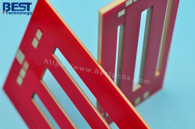
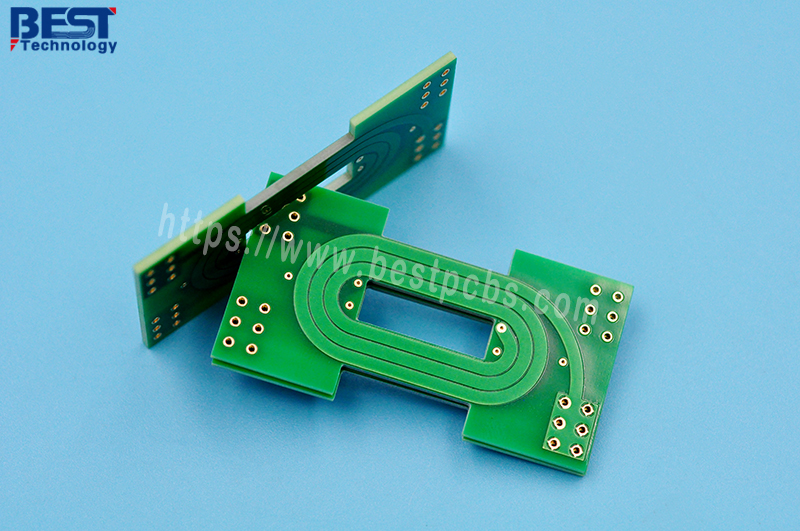
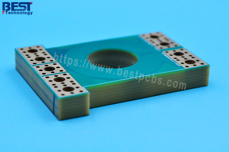
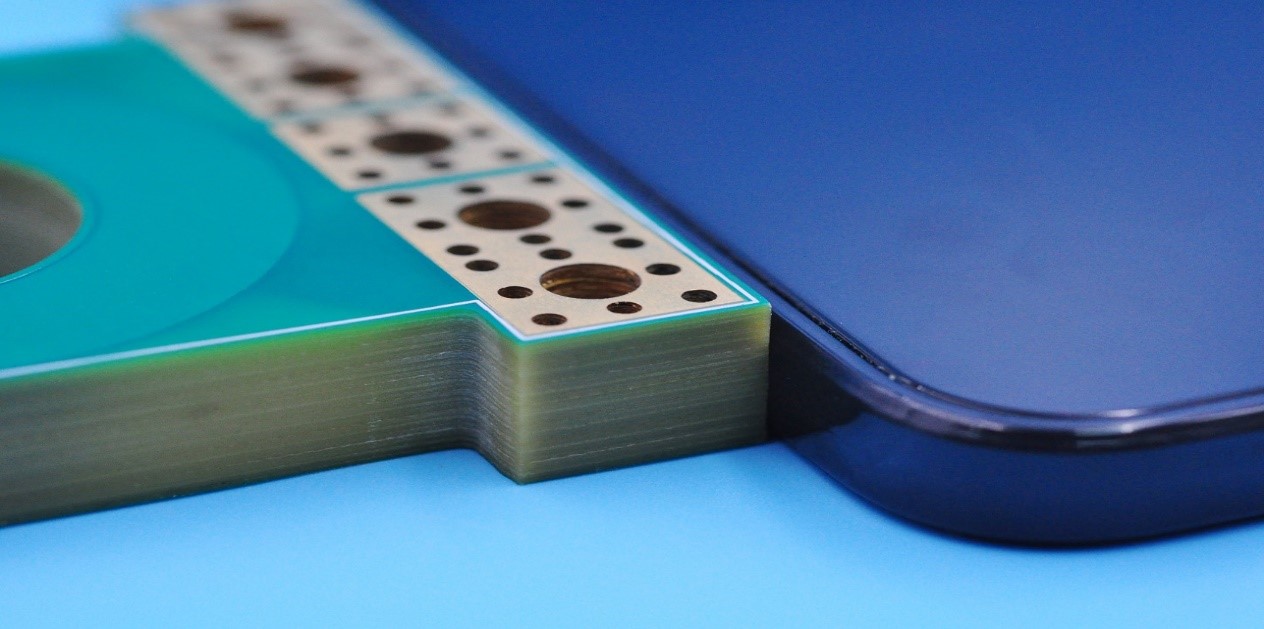
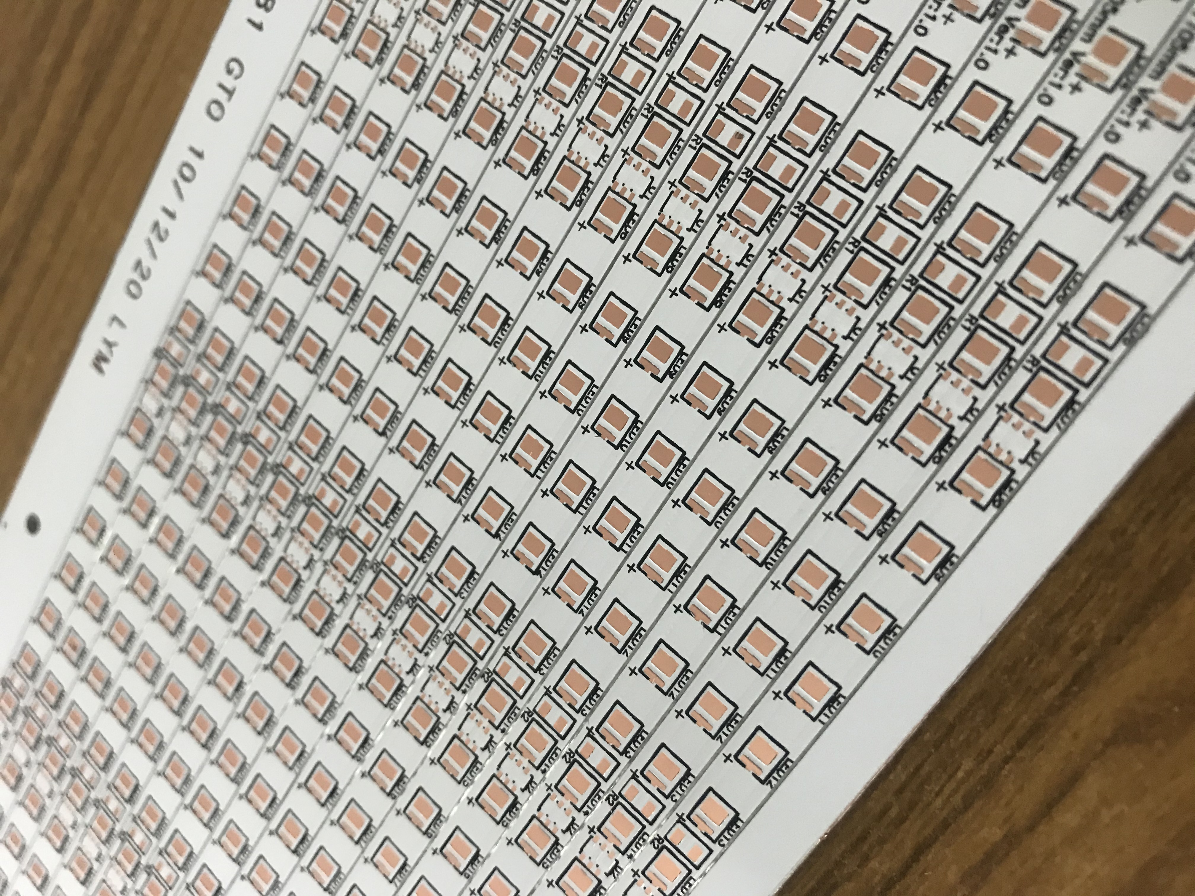
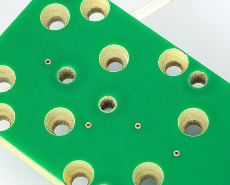
A counterbore is a cylindrical, flat-bottomed hole that is strategically cut into a material to accommodate specific components or fasteners. It is commonly used in various industries, including woodworking, metalworking, and mechanical engineering. The purpose of a counterbore is to create a recessed area where a component, such as a bolt head, nut, or other hardware, can sit flush with or below the surface of the material. This technique ensures a smooth appearance, prevents interference with other components, and provides mechanical stability.

Counterbores in PCB Design and Manufacturing
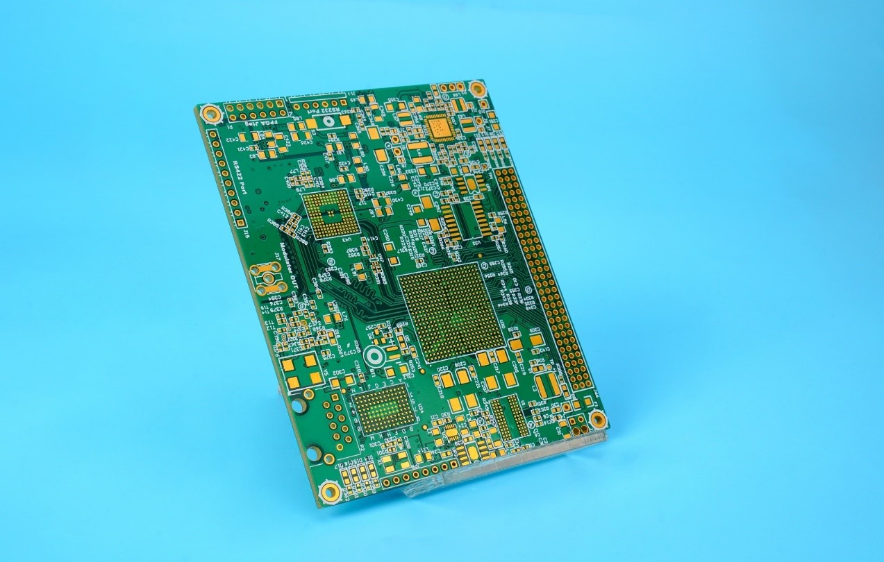
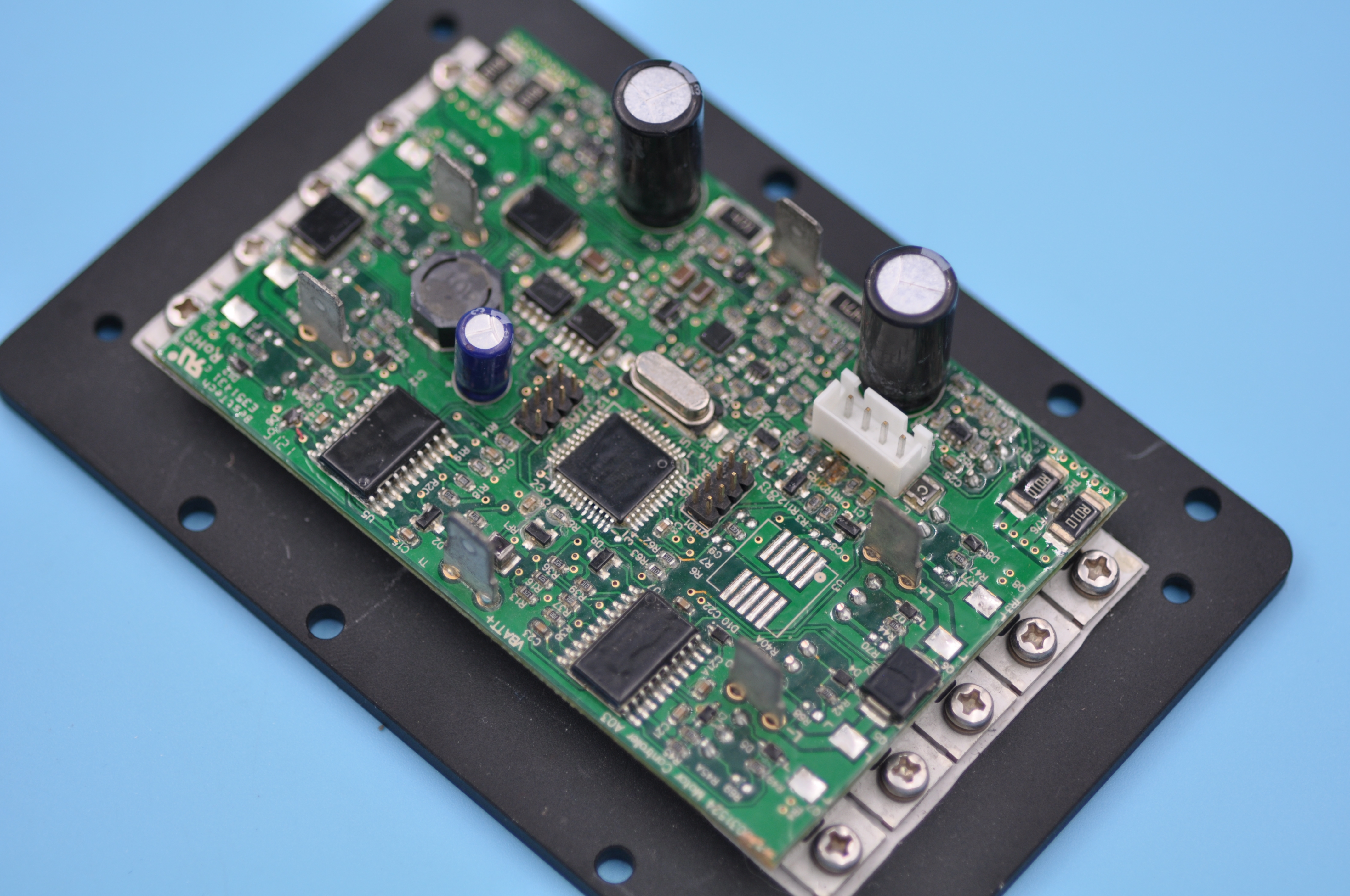
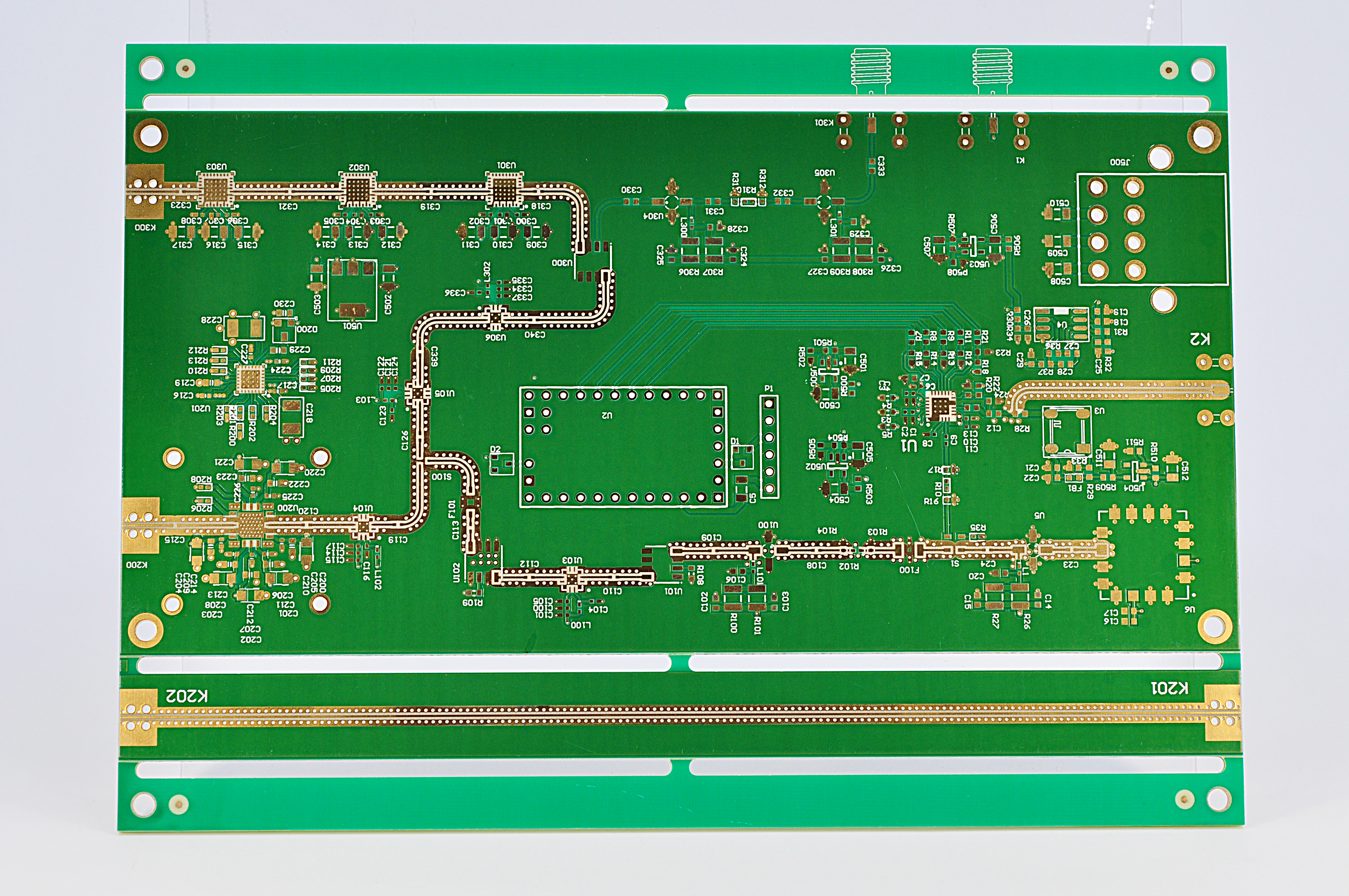
In the realm of printed circuit boards (PCBs), counterbores play a crucial role in achieving efficient and functional designs. PCBs are essential components in electronic devices, and their design requires careful consideration of component placement, connectivity, and mechanical stability. Counterbores in PCBs serve several important functions:
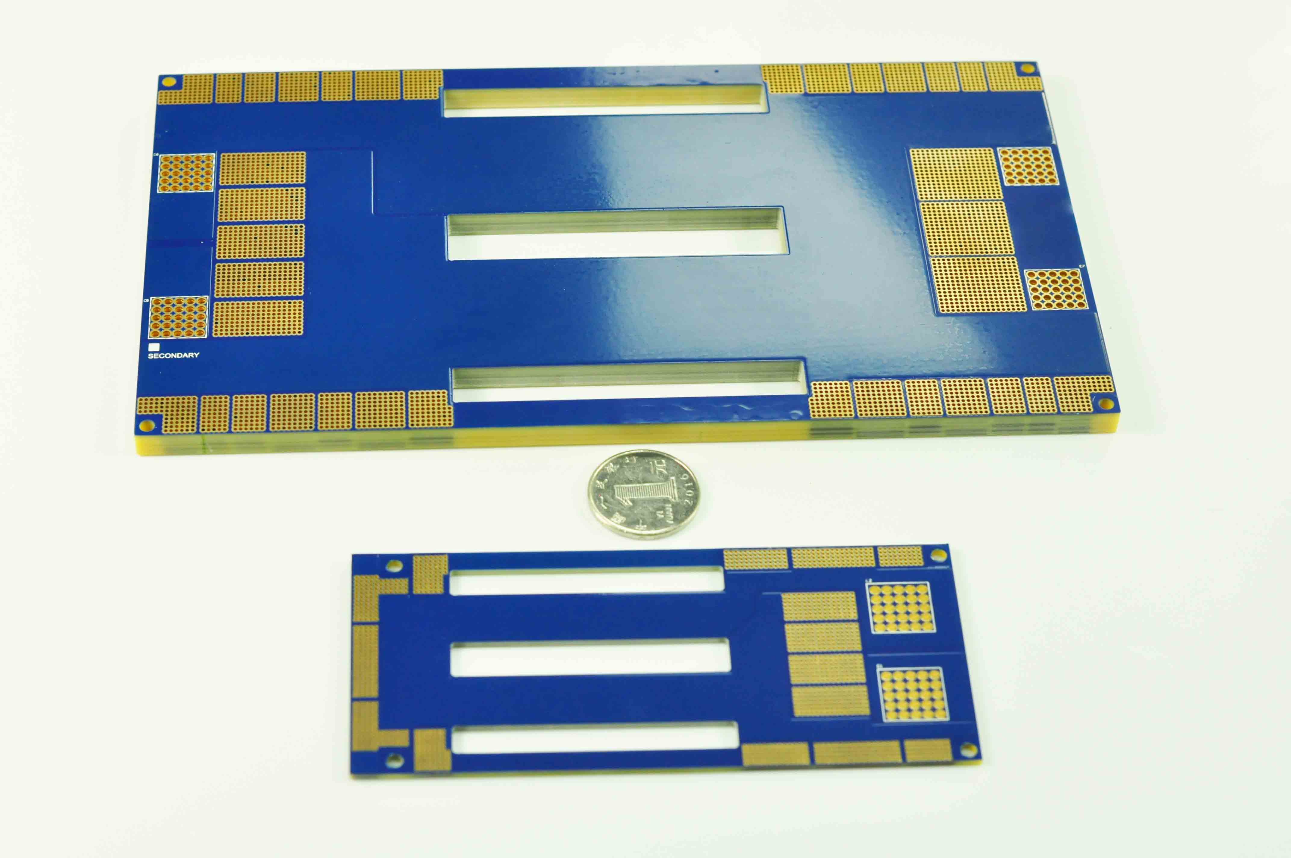
- Component Alignment and Clearance: Certain components on a PCB, such as connectors, switches, or specialized modules, require precise alignment and clearance for optimal functionality. A counterbore can be introduced to create a recessed area that accommodates these components, ensuring proper alignment with neighboring components and minimizing the risk of interference.
- Flush Mounting: To maintain a sleek and compact design, some components need to be mounted flush with the surface of the PCB. A counterbore creates a flat-bottomed recess that allows the component to sit at the same level as the PCB surface, contributing to an aesthetically pleasing and functional layout.
- Mechanical Support: Components that are susceptible to mechanical stress or impact may benefit from additional support. By incorporating a counterbore, the PCB design can provide a more secure location for these components, reducing the risk of damage.
- Heat Dissipation Enhancement: In applications where certain components generate significant heat, such as power amplifiers or processors, heat sinks are often employed to dissipate the heat. A counterbore can facilitate proper alignment and contact between the heat sink and the component, optimizing heat transfer and overall thermal performance.
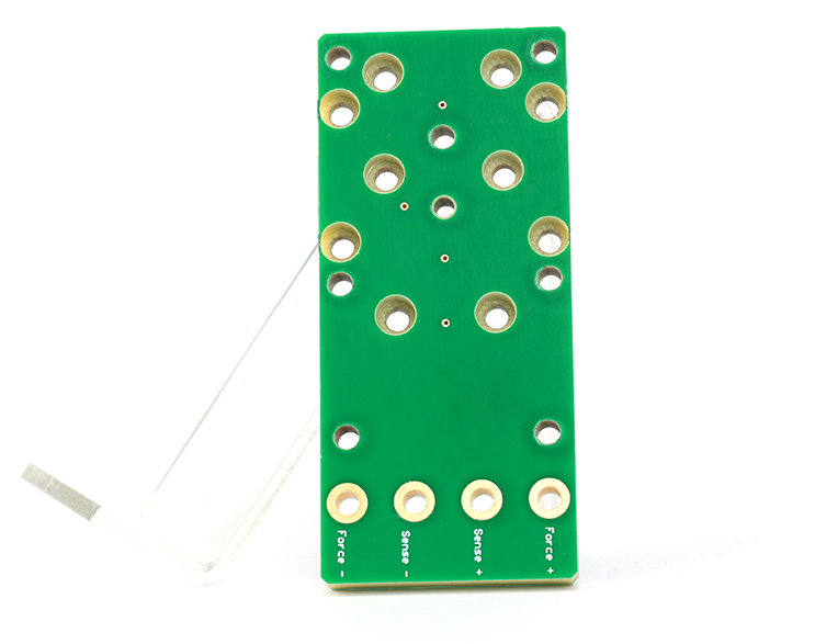
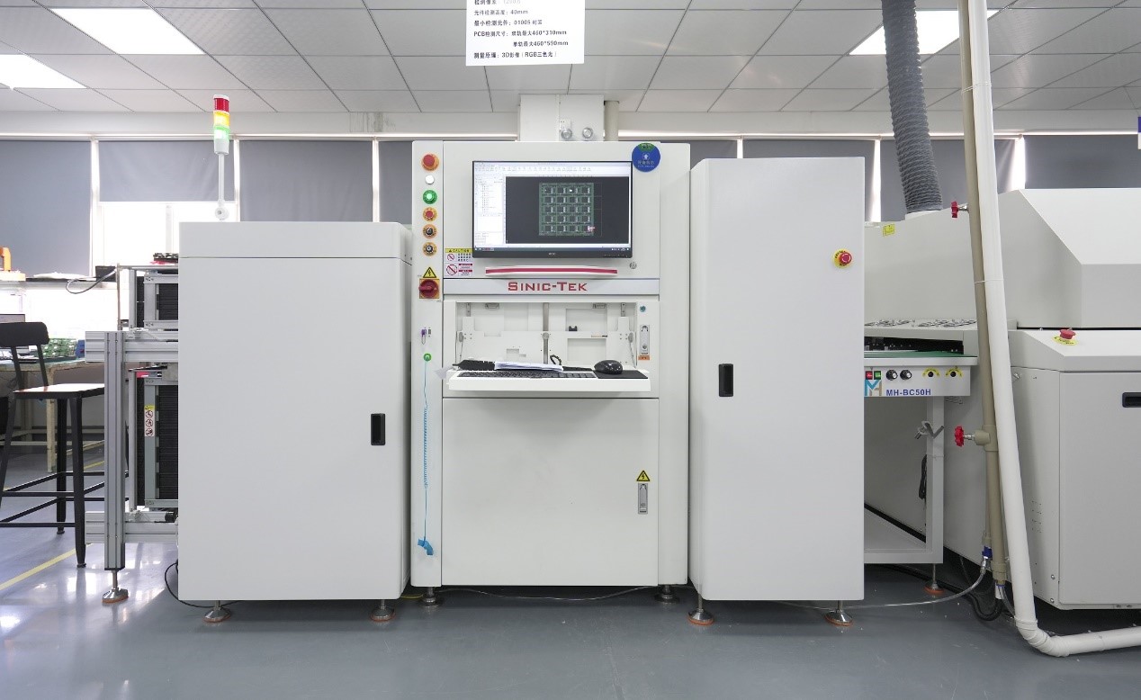
The production of counterbores in PCBs involves specialized manufacturing techniques. BEST Technology as a professional PCB manufacturer, we will use precision drilling and routing equipment to create accurately sized and positioned counterbores.
If you want to know more about the counterbores, welcome to follow our post or contact us.