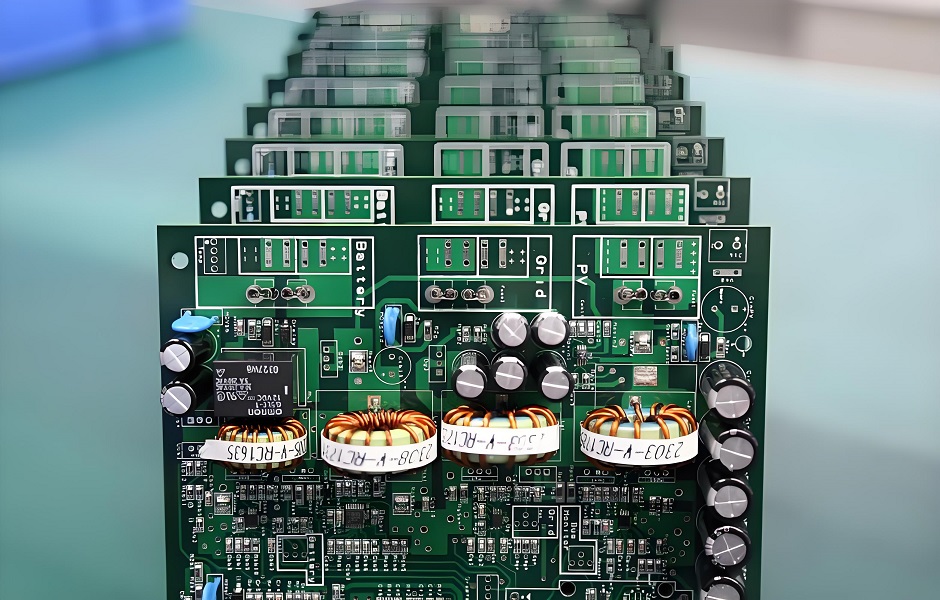
Ceramic printed circuit board is a PCB made with a ceramic base instead of resin. Its main strength is fast heat transfer, which keeps components cooler and more stable. Because ceramic handles high power and tough environments well, it’s used in LEDs, automotive systems, medical devices, and high-frequency electronics.
What Is a Ceramic PCB?
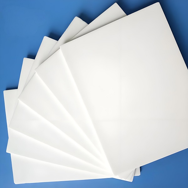
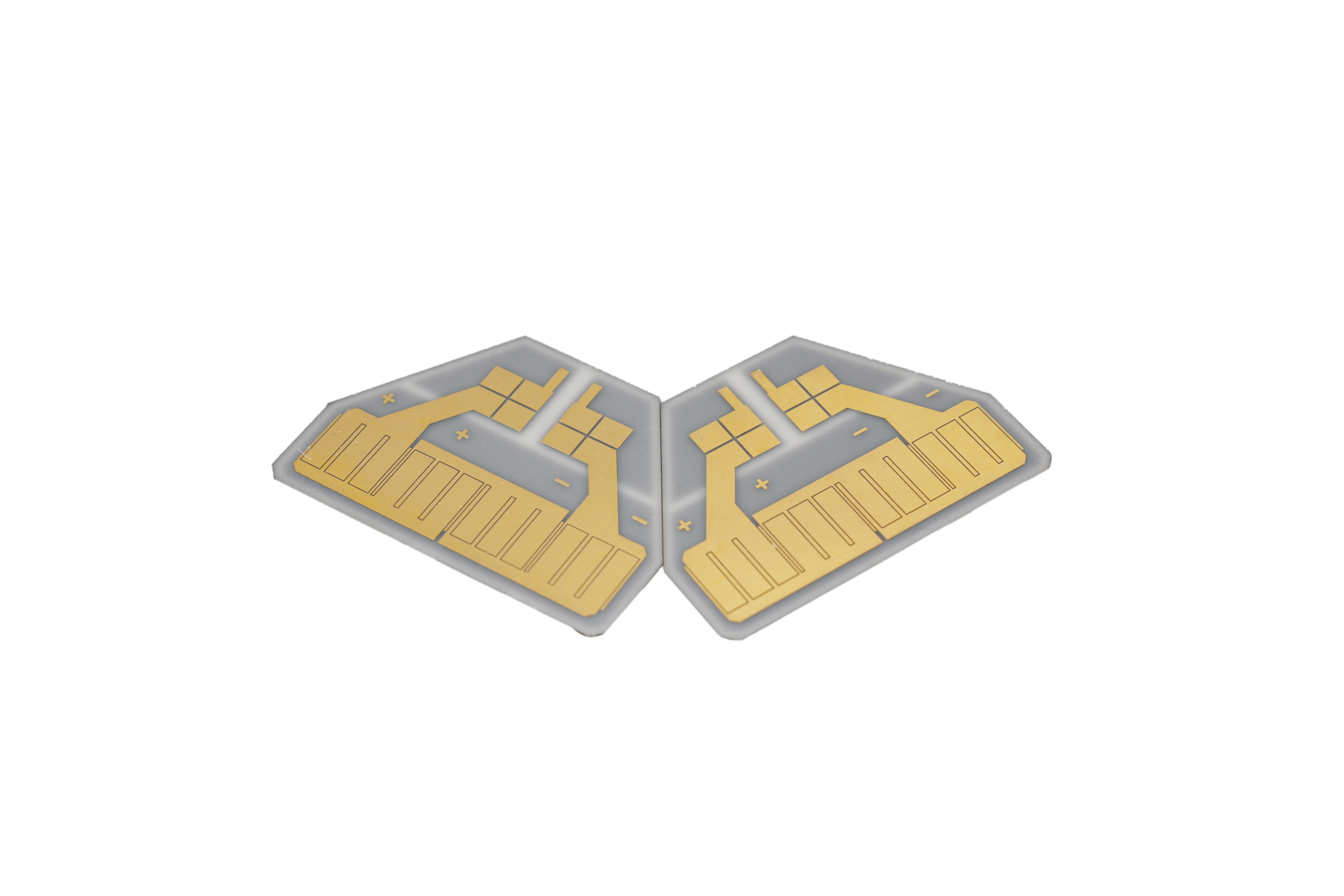
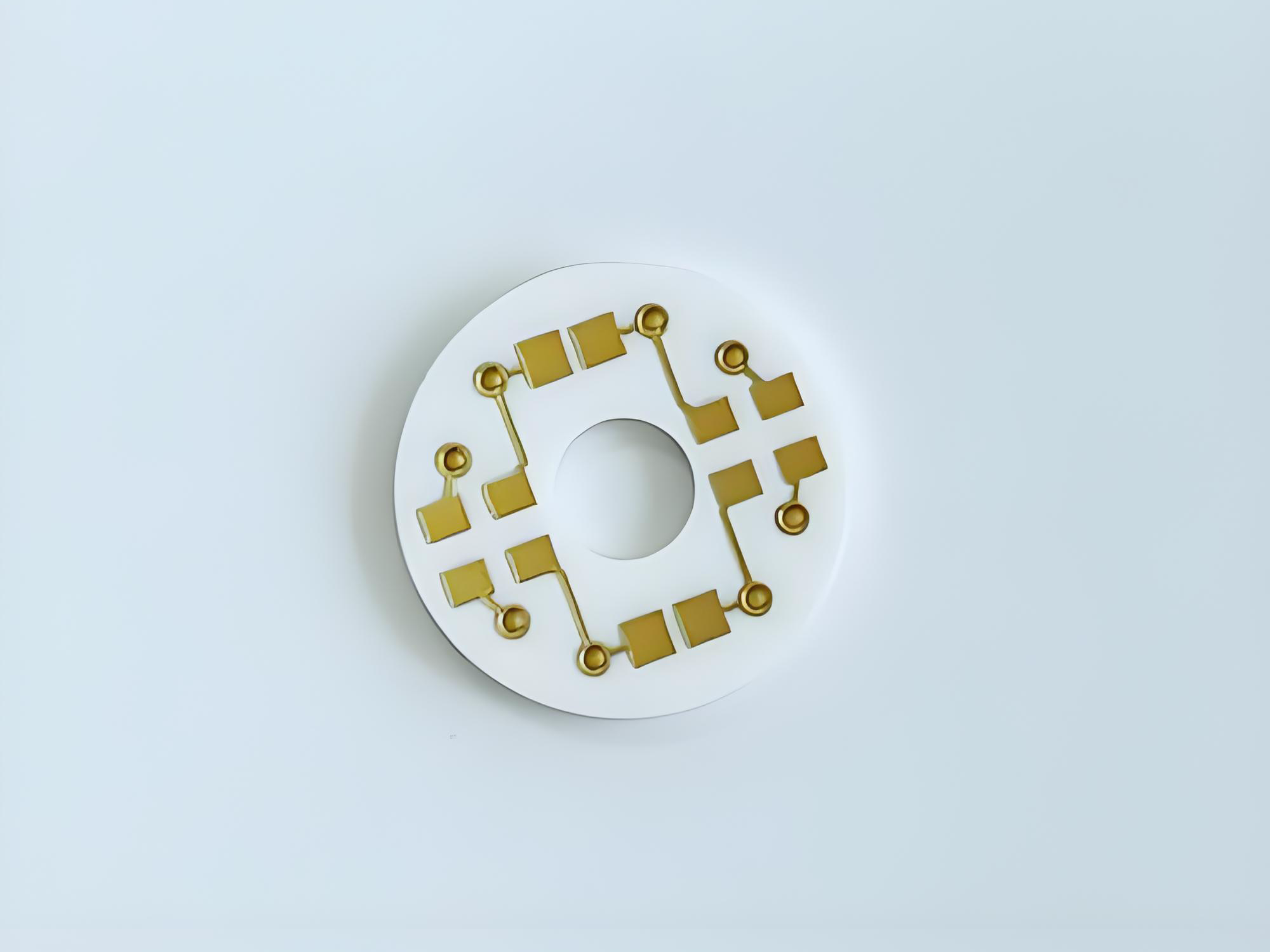
Ceramic printed circuit board is a board made from ceramic materials instead of traditional resin-based laminates. Ceramic materials have a natural ability to handle heat. They move heat away from components fast, which protects sensitive parts during operation.
This type of board uses ceramic as the base. Common ceramic materials include alumina, aluminum nitride, and beryllium oxide. Each type has its own strengths. All of them offer stable performance, steady conductivity, and strong durability.
Ceramic PCBs are built for harsh work. They stay stable even when temperatures climb high. This makes them a top choice for applications that demand reliability.
Ceramic printed circuit boards also carry strong mechanical strength. They resist stress and remain stable when exposed to vibration.
Are Ceramic PCBs Expensive?
Ceramic PCBs have extremely high performance. Because of this, many people assume they cost more. Ceramic board price can be higher than common materials. But this cost comes with advantages that help reduce risks in the long run.
Ceramic boards help lower failure rates. They also support higher power levels. They reduce heat-related damage.
Many ceramic printed circuit board manufacturers now offer cost-effective options. Improved production methods have made ceramic PCBs more accessible. As technology grows, the price gap continues to shrink.
So yes, ceramic PCBs can be more expensive, but the value is strong. They bring stable and safe performance that protects the final product.
What Affects Ceramic Board Price?
Ceramic board price depends on several factors. Each factor influences the final cost.
- 1. Material Type
Different ceramic materials have different costs. Aluminum nitride, for example, offers very high thermal conductivity. Because of this, it often costs more. Alumina is more affordable and works well for many applications.
- 2. Board Thickness
Thicker boards use more material. This increases the price.
- 3. Layer Count
A single-layer ceramic PCB costs less than a multilayer design. Multilayer boards need extra processes and bonding methods. This adds complexity and raises cost.
- 4. Conductive Layer
Ceramic PCBs use thick-film or thin-film metallization. Each method has its own cost. Silver, gold, and copper can also influence the total price.
- 5. Manufacturing Technology
Ceramic PCBs require special equipment. Some boards need laser cutting. Some need advanced firing ovens.
- 6. Design Complexity
A simple design is cheaper. A design with dense pads, small traces, and tight spacing costs more.
- 7. Order Quantity
Large orders usually cost less per unit. Smaller orders can be more expensive.
- 8. Surface Treatment
Extra surface finishes add cost. Gold plating or special coatings improve durability and performance, but they also increase the price.
- 9. Testing Requirements
Some industries need strict tests. These tests help ensure quality. Extra testing adds cost but provides more assurance.
Even with these factors, ceramic board price has become more competitive. Many ceramic printed circuit board factories offer flexible options to fit different budgets.
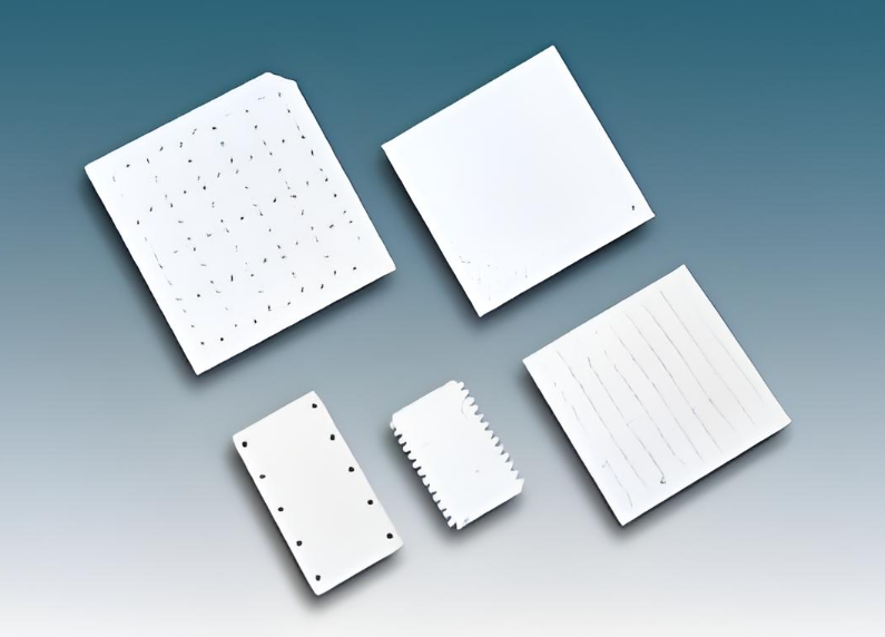
What Are the Types of Ceramic Circuit Board?
Ceramic circuit boards come in several types. Each one supports different needs.
- Thick-Film Ceramic PCB: Conductive paste is printed onto the ceramic surface. It offers stable performance at a reasonable cost.
- Thin-Film Ceramic PCB: Thin-film boards offer high precision. They use vacuum deposition to create fine lines.
- DBC (Direct Bonded Copper) Ceramic PCB: In this type, copper is bonded directly to the ceramic. It offers incredible thermal performance.
- DPC (Direct Plated Copper) Ceramic PCB: DPC boards use laser drilling and plating. They can achieve very fine lines.
- Hybrid Ceramic PCB: This type combines ceramic and other materials. It improves performance while keeping cost flexible.
Each type has its own unique benefits. The specific choice depends on your application and design requirements.
How Does a Ceramic Printed Circuit Board Work?
Ceramic printed circuit boards work by carrying signals and power across conductive layers on a ceramic base. The ceramic material holds the circuit firmly and keeps heat under control.
Heat moves through ceramic at a fast rate. This keeps components cool. The stable base also prevents bending, which helps protect tiny circuit paths.
The conductive layer, whether thick-film or thin-film, passes signals without losing accuracy. Ceramic material supports smooth transmission.
When power increases, ceramic handles the stress. Its high thermal conductivity spreads heat quickly. This helps maintain stable performance even under heavy load.
Because of this balance of temperature management and strong reliability, ceramic printed circuit boards support long-term use without problems.
Why Use a Ceramic Base Print Circuit Board?
Ceramic base print circuit board brings solid benefits. They were chosen because of their good stability, good heat dissipation, and long service life.
Ceramic boards protect components from heat. They keep signals clean. They support high-power loads without losing accuracy. Because they resist chemicals and moisture, they also stay strong in demanding environments.
What Are the Advantages of Ceramic Printed Circuit Boards?
Ceramic PCBs offer numerous advantages because they provide reliable and robust performance.
- 1. Excellent Thermal Conductivity
Ceramic moves heat fast. This helps cool components. It also reduces heat-related problems.
- 2. High Mechanical Strength
Ceramic materials resist stress. They do not deform easily. This helps protect the circuit.
- 3. Stable in Harsh Environments
Ceramic stays strong even when temperatures rise. It also resists chemicals and moisture.
- 4. Long Lifespan
Ceramic PCBs last a long time. They support heavy-duty work without breaking down.
- 5. Low Dielectric Loss
This feature helps improve signal quality. Many RF devices rely on this benefit.
- 6. Strong Reliability
Ceramic printed circuit boards offer stable and predictable performance. They help reduce unexpected issues.
- 7. Compact Design Possibility
They support high-density layouts. This helps shrink overall product size.
What Is the Difference Between Ceramic PCB and FR4?
Ceramic and FR4 have different qualities. Each one serves a specific purpose.
- 1. Thermal Performance
Ceramic handles heat much better. FR4 cannot match ceramic in this area. Devices that generate strong heat prefer ceramic.
- 2. Mechanical Strength
Ceramic has stronger stability. FR4 is easier to bend. Ceramic protects the circuit better in tough environments.
- 3. Electrical Properties
Ceramic has better dielectric performance. It helps support high-frequency signals with lower loss.
- 4. Cost
FR4 is cheaper. Ceramic costs more but offers better performance.
- 5. Application Field
FR4 works well for common devices. Ceramic is used for high-end, high-power, and high-temperature applications.
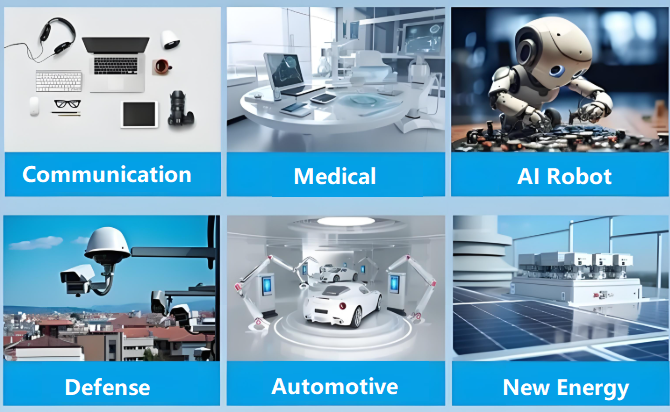
Where Are Ceramic Printed Circuit Boards Used?
Ceramic printed circuit boards are used in many advanced applications. Their strength and heat-handling ability make them ideal for demanding work.
- LED Lighting Systems: High-power LEDs use ceramic boards to stay cool. This helps extend LED lifespan.
- Automotive Electronics: Ceramic PCBs support engine control units, sensors, and power modules. They can handle vibration and heat.
- Medical Devices: Medical tools need stable circuits. Ceramic PCBs support imaging equipment and diagnostic devices.
- Aerospace Systems: Ceramic offers strong reliability. Aircraft and satellites depend on stable performance in extreme conditions.
- Power Electronics: Devices that handle high power depend on ceramic. The material helps reduce heat and improve safety.
- Communication Devices: High-frequency modules use ceramic because of its low dielectric loss.
- Industrial Control: Robotic systems and automation equipment rely on ceramic PCBs for safe performance.
These industries trust ceramic because it delivers powerful and dependable results.
What Materials Do Ceramic Printed Circuit Board Manufacturers Use?
Ceramic printed circuit board manufacturers use several popular materials. Each one supports different needs.
- 1. Alumina (Al₂O₃)
This is the most common ceramic material. It offers balanced cost and performance.
- 2. Aluminum Nitride (AlN)
This material has high thermal conductivity. It handles heat extremely well. It is ideal for high-power devices.
- 3. Beryllium Oxide (BeO)
BeO offers excellent heat performance. It is used less often because of handling restrictions. Some high-end applications still use it.
- 4. Zirconia
Zirconia offers high strength. It is used for certain structural needs.
BEST Technology will select materials based on your requirements. We will consider heat resistance, strength, cost, and performance. This ensures the final product meets your expectations.
How to Manufacture Ceramic Printed Circuit Board?
Ceramic PCB manufacturing involves several steps. Each step ensures quality and stability.
- Material Preparation: Ceramic sheets are prepared in controlled environments. They must be clean and smooth.
- Metallization: Conductive layers are added. This can be done through thick-film or thin-film processes. The metallization forms the circuit traces.
- Printing: For thick-film boards, conductive paste is printed onto the ceramic surface. Precision is important.
- Firing: The board is placed in a high-temperature oven. This step sinters the material and bonds the traces securely.
- Laser Machining: Some designs need small holes or fine cuts. Lasers provide accurate shaping.
- Plating and Surface Finish: Surface finishes improve reliability. They also protect the surface.
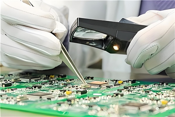
- Testing: Each board is tested to ensure proper performance.
- Final Inspection: We will inspect the circuit boards, including alignment, trace quality, and strength.
Conclusion:
Ceramic printed circuit board offers powerful performance, fast heat transfer, strong mechanical durability, and stable electrical properties. It supports high-power systems, advanced sensors, medical devices, LED technology, and automotive electronics. While ceramic board price can be higher than standard boards, the value is strong.
If you need high-quality ceramic printed circuit boards or want a quote, feel free to contact: sales@bestpcbs.com