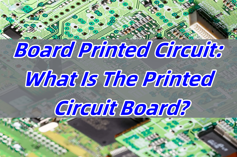
What is pcb sbu technology? SBU technology in PCB refers to “Sequential Build Up”, which is a technology used to manufacture high-density interconnect (HDI) multi-layer PCBs. It achieves higher wiring density and smaller board size by stacking additional conductive and insulating layers layer by layer on the basis of traditional multi-layer boards and using micro-vias (blind or buried vias) to achieve inter-layer connections.
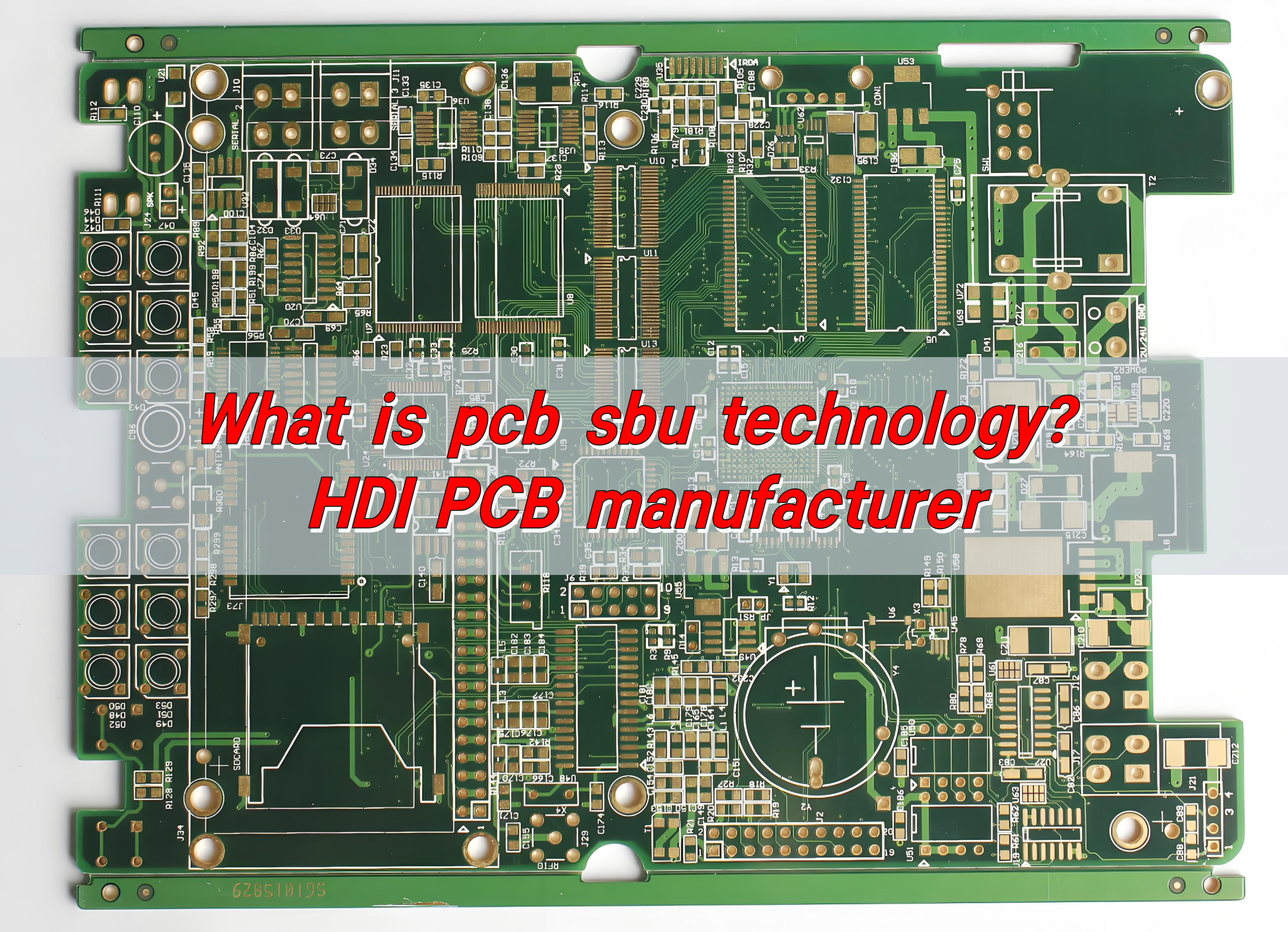
What is pcb sbu technology?
PCB SBU technology stands for Sequential Build Up technology. It is an advanced process used in the manufacturing of high-density interconnect (HDI) PCBs.
This technique involves building up multiple layers of a PCB in a sequential manner, typically starting from the inner layer and adding layers progressively.
Each layer is added using specialized processes that make it possible to create smaller vias, more complex routing, and finer features compared to traditional PCB manufacturing.
SBU technology is essential in HDI PCB production, which is commonly used in devices that require high performance in a compact form factor, such as smartphones, medical devices, automotive electronics, and other modern electronic systems.
By using SBU technology, multiple layers can be stacked with precision while maintaining the electrical performance and signal integrity required by these applications.
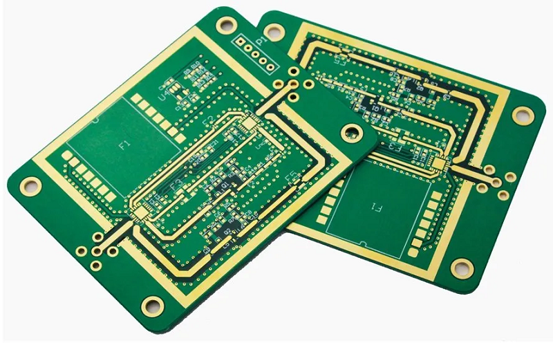
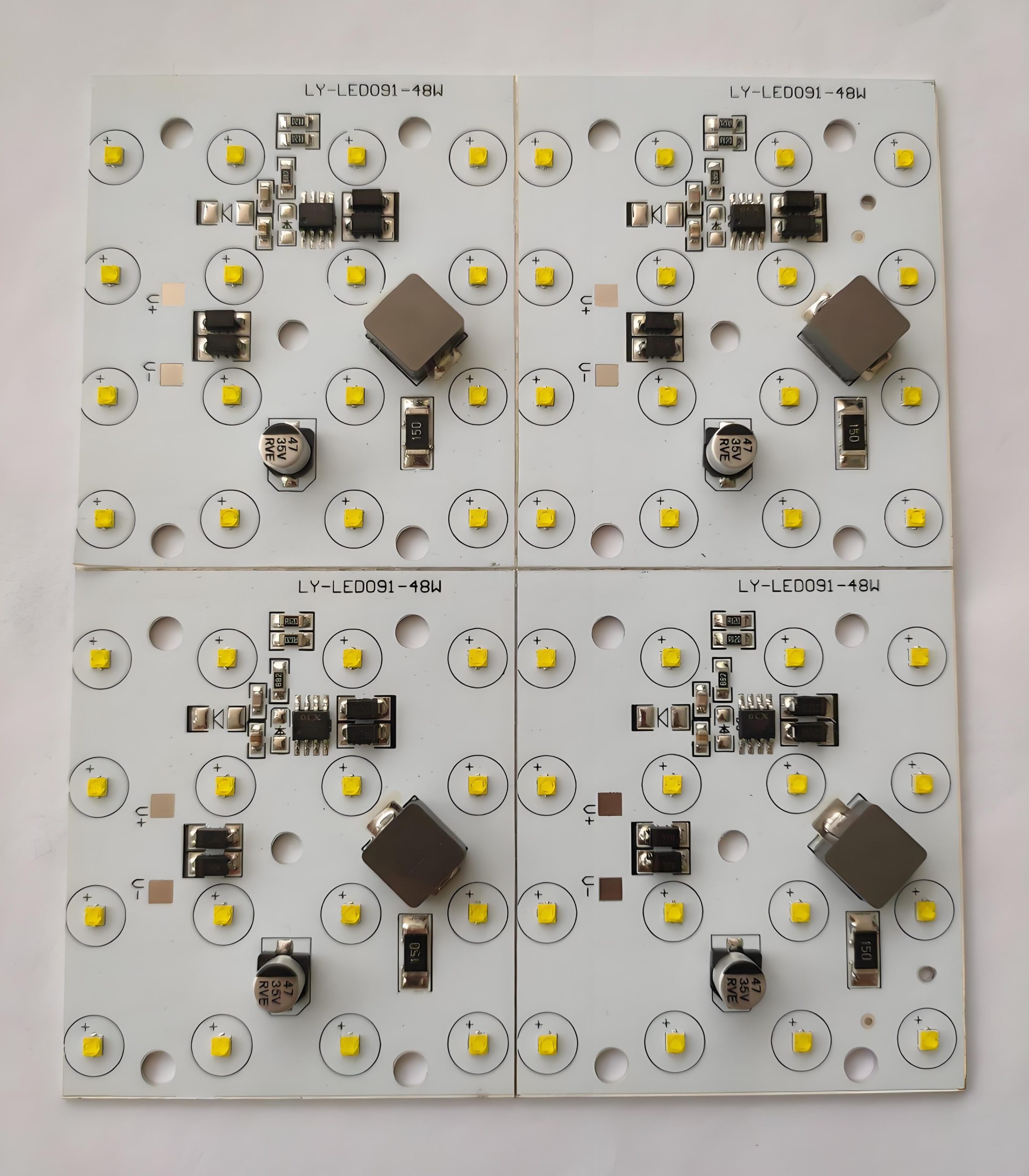
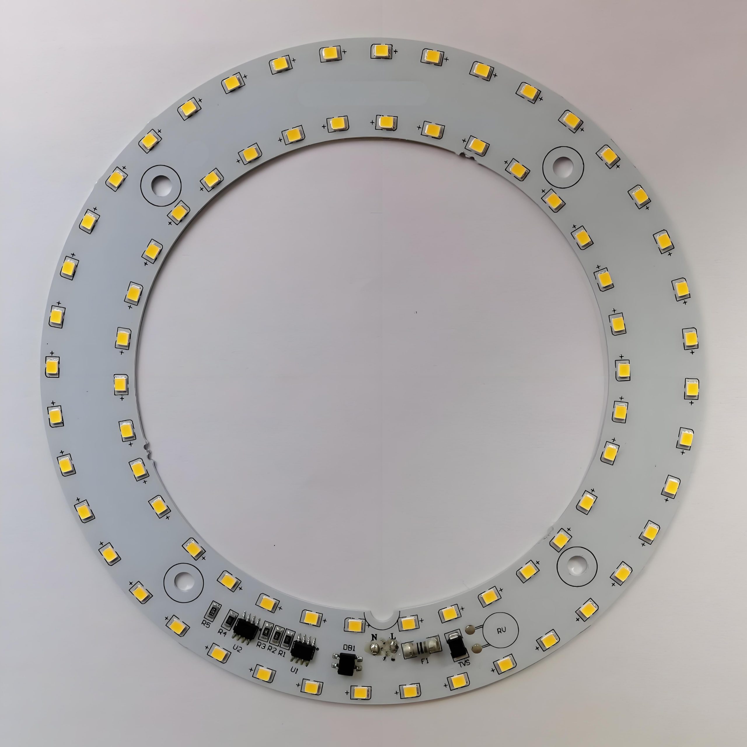
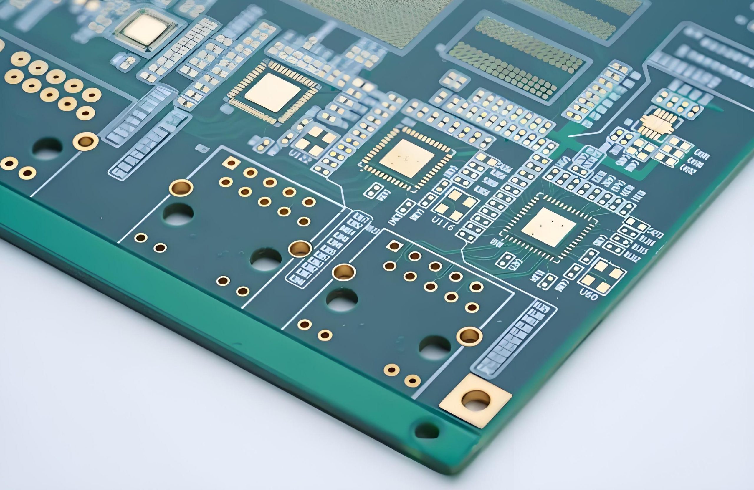
What is HDI PCB?
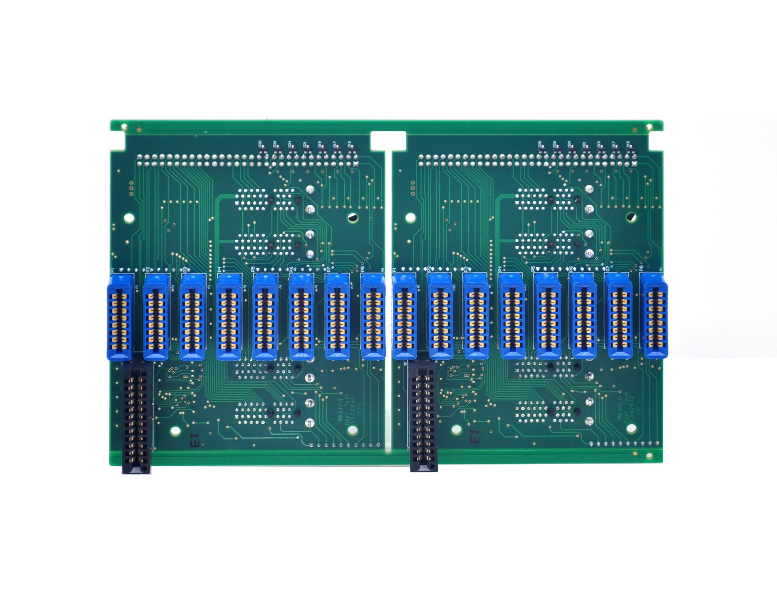
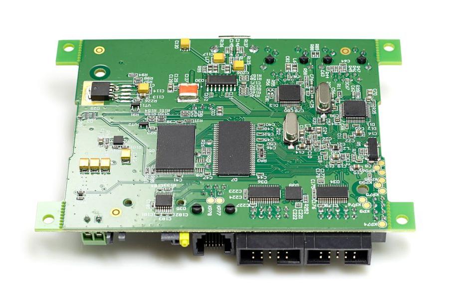
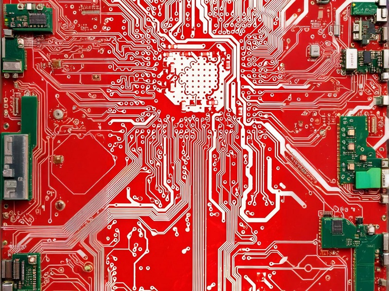
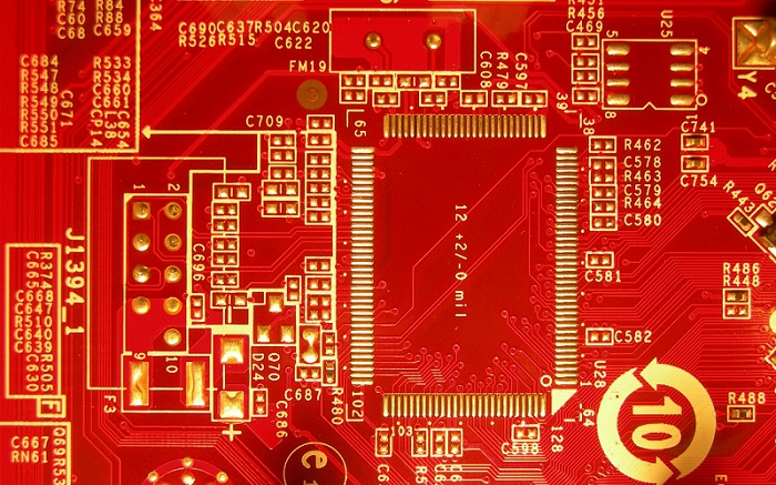
An HDI PCB (High-Density Interconnect PCB) is a type of printed circuit board that offers higher density and more compact designs.
HDI PCBs are designed to handle fine-pitch components, high-frequency signals, and miniaturized electronic devices. They use advanced manufacturing techniques such as microvias, blind vias, and buried vias, making them the preferred choice for high-performance applications.
HDI boards are typically characterized by:
- Smaller and finer traces – Supporting higher component density.
- Microvias – Very small holes used to connect different layers in the PCB.
- Blind and buried vias – Vias that only connect specific layers, improving space utilization.
- Stacked or staggered via construction – For reducing board size and increasing routing flexibility.
By leveraging HDI technology, manufacturers can create more compact and efficient PCBs that perform exceptionally well in the most demanding electronic applications.
What is a buried hole?
A buried hole is a via that connects two inner layers of a PCB but does not go through the entire thickness of the board. These vias are entirely enclosed within the PCB layers and are not visible on the outer surfaces.
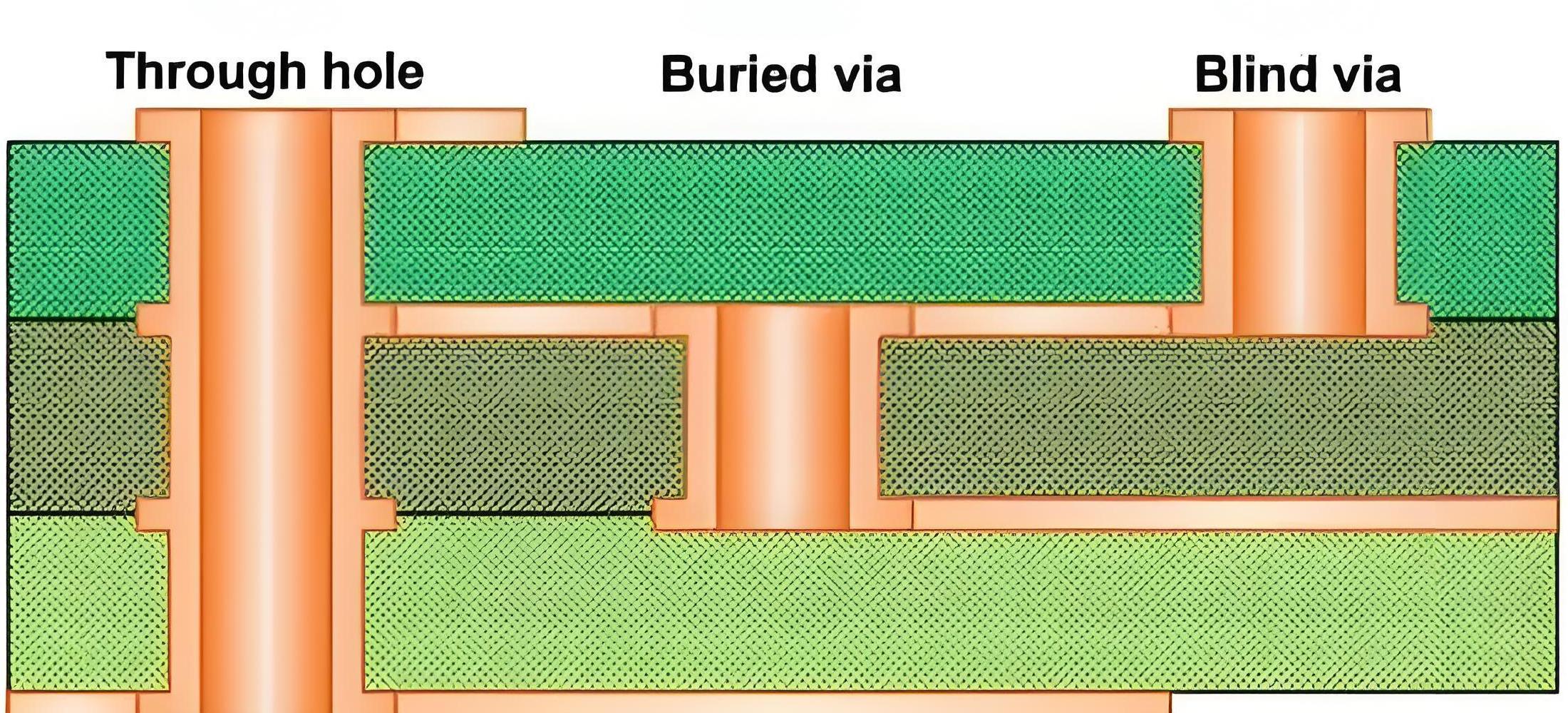
Buried holes are commonly used in HDI designs to enable multi-layer connections while optimizing the space on the outer layers for components and routing.
How Buried Holes Benefit PCB Design:
- Maximized board space – Since they don’t take up space on the outer layers.
- Reduced signal interference – By isolating inner-layer connections from the external surface.
- Improved electrical performance – Essential for high-speed, high-frequency designs.
Buried holes are particularly beneficial in high-performance electronic devices that require dense component placement without compromising the integrity of the signal paths.
What is a blind hole?
A blind hole is a via that connects an outer layer to one or more inner layers of the PCB, but does not extend all the way through the board.
It is “blind” because it doesn’t go all the way through the PCB like a through-hole. These types of vias are often used when connections need to be made between surface components and inner layers without occupying precious outer-layer space.
Benefits of Blind Holes:
- Space-saving – No need for holes that go all the way through the board.
- Enhanced routing flexibility – Allows for more efficient use of the board’s surface.
- Reduced component size – Perfect for designs with high-density components that need a compact form.
Blind vias help ensure that HDI boards can be designed with multiple layers, allowing for more complex circuits without increasing board size. They are ideal for devices with multi-functional, high-density circuit layouts.
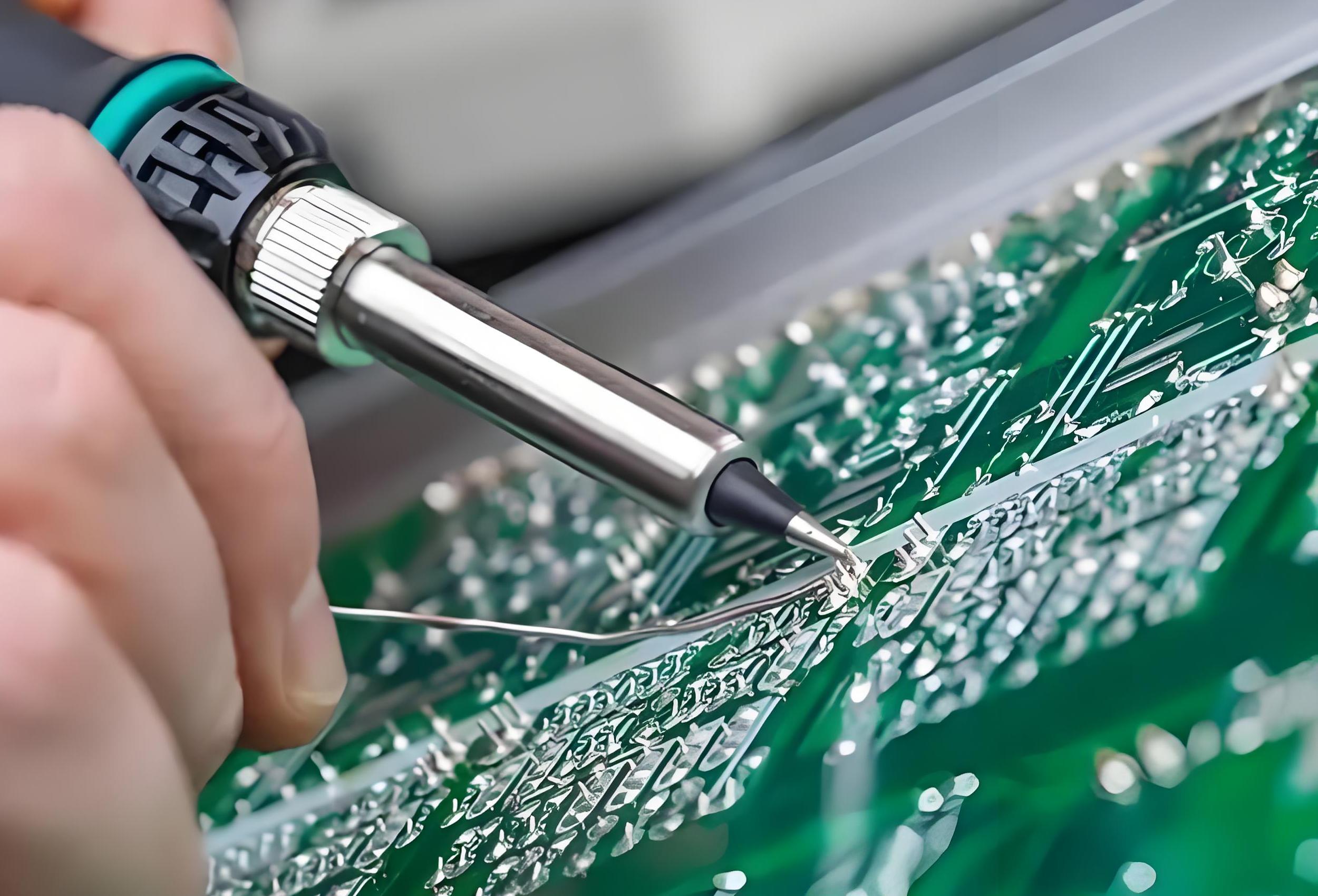
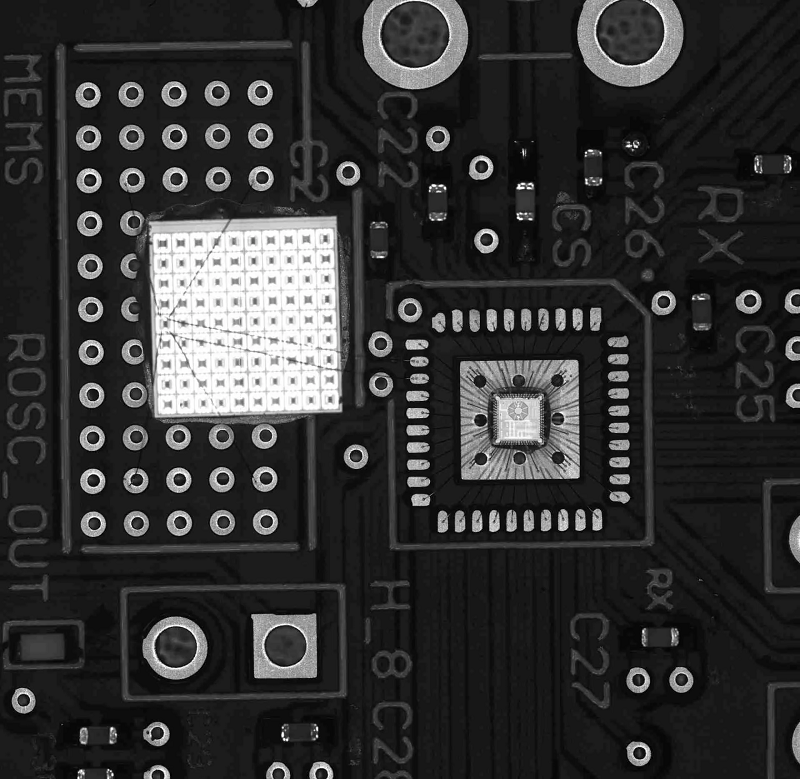
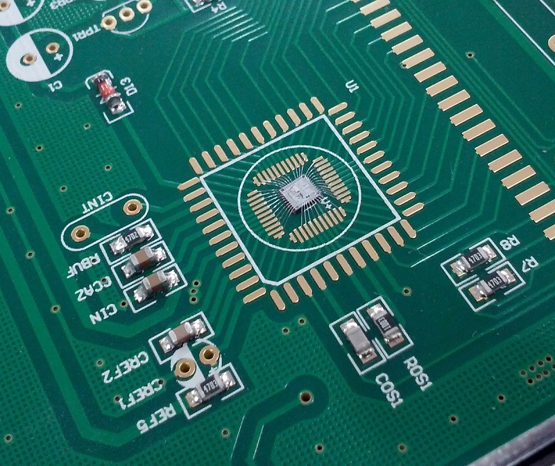
What is a microvia?
A microvia is a very small via used in HDI PCB designs to create electrical connections between the layers. Microvias are typically laser-drilled, allowing for precise and tiny holes that are ideal for high-density applications.
They generally have a diameter of less than 150 microns, making them perfect for high-frequency, high-speed circuits that need to minimize space without sacrificing performance.
Key Advantages of Microvias:
- Reduced board size – Enables more compact designs without compromising performance.
- Improved electrical performance – Allows for shorter signal paths and fewer signal losses.
- Better signal integrity – Minimizes the risk of signal interference and distortion.
- Enhanced routing flexibility – Provides designers with more options for creating high-density, complex circuits.
Microvias are indispensable for modern PCB designs that demand high performance, miniaturization, and advanced electrical features.
What are the advantages of Sbu technology?
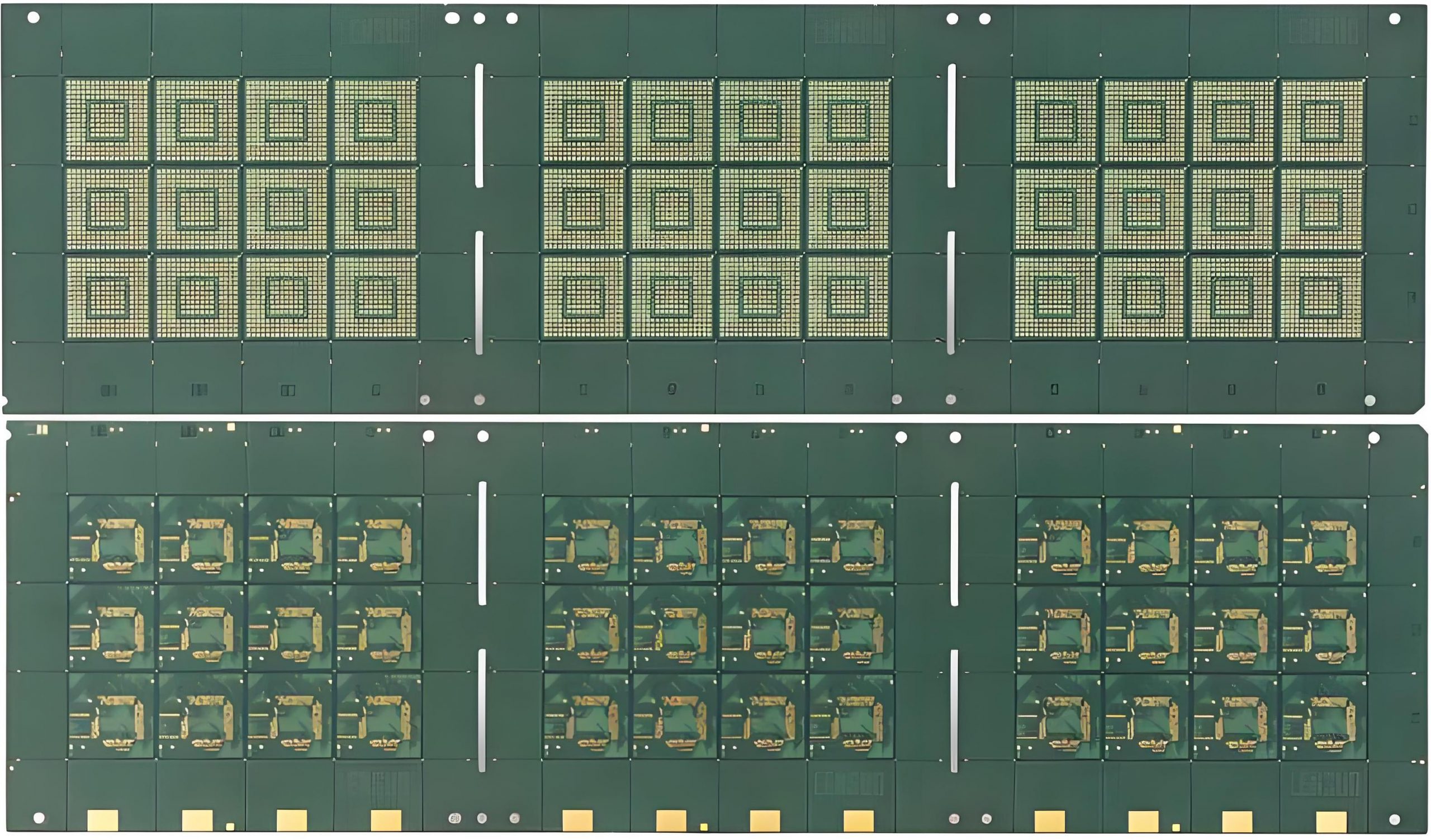
Sequential Build-Up (SBU) technology offers several key advantages, especially in the production of HDI PCBs.
By allowing for the precise construction of multi-layered boards with intricate features, SBU technology helps manufacturers achieve designs that would be impossible with traditional PCB technologies.
Key Benefits of SBU Technology:
Enhanced Performance in Smaller Footprints – By using fine-pitch components, microvias, and blind or buried vias, SBU technology enables the creation of small, highly efficient circuits.
- Faster Production Cycle – The sequential build-up process reduces the overall time required to produce multi-layer boards compared to conventional methods.
- Cost-Effective for Prototyping – Ideal for low to medium-volume runs, where modifications can be made quickly without the need for large-scale tooling changes.
- Better Signal Integrity – The small via sizes and precise routing make SBU technology particularly effective for high-speed, high-frequency designs.
- Flexibility in Layer Design – SBU allows for a more flexible design process, offering greater options in terms of layer stack-ups and via types.
Overall, SBU technology empowers PCB designers to achieve advanced, high-performance circuits while maintaining cost-effectiveness and design flexibility.
What is the difference between PCB substrate and laminate?
The terms substrate and laminate are often used interchangeably in the context of PCB manufacturing, but they refer to different parts of the PCB construction process.
- Substrate – The substrate is the core material of the PCB. It is typically made of fiberglass (FR4) or ceramic and provides the foundational structure on which the circuit layers are built.
- Laminate – A laminate refers to the outer layer material that is bonded to the substrate. It is often a combination of resins and copper foil.
Key Differences:
Substrate is the primary base material, while laminate is used to build up the layers on top of the substrate.
Substrate provides mechanical support, whereas laminate contributes to the board’s electrical properties.
Both are crucial components in the production of HDI PCBs and other advanced circuit boards, ensuring strength, reliability, and functionality.
What is the difference between PCB and package substrate?
The main difference between a PCB substrate and a package substrate lies in their intended function and design:
- PCB Substrate – Primarily used for circuit boards, these substrates provide structural support for the PCB’s electrical connections.
- Package Substrate – This is used in chip packaging and provides connections between the chip and the external circuit.
The PCB substrate is mainly concerned with signal routing and electrical connections, while the package substrate focuses more on chip integration and interfacing with external systems.
Conclusion:
PCB SBU technology has revolutionized the way high-density interconnect (HDI) PCBs are designed and manufactured.
At EBest Circuit (Best Technology), we leverage our extensive expertise and advanced manufacturing capabilities to produce top-tier HDI PCBs with SBU technology. For inquiries, contact us at: sales@bestpcbs.com