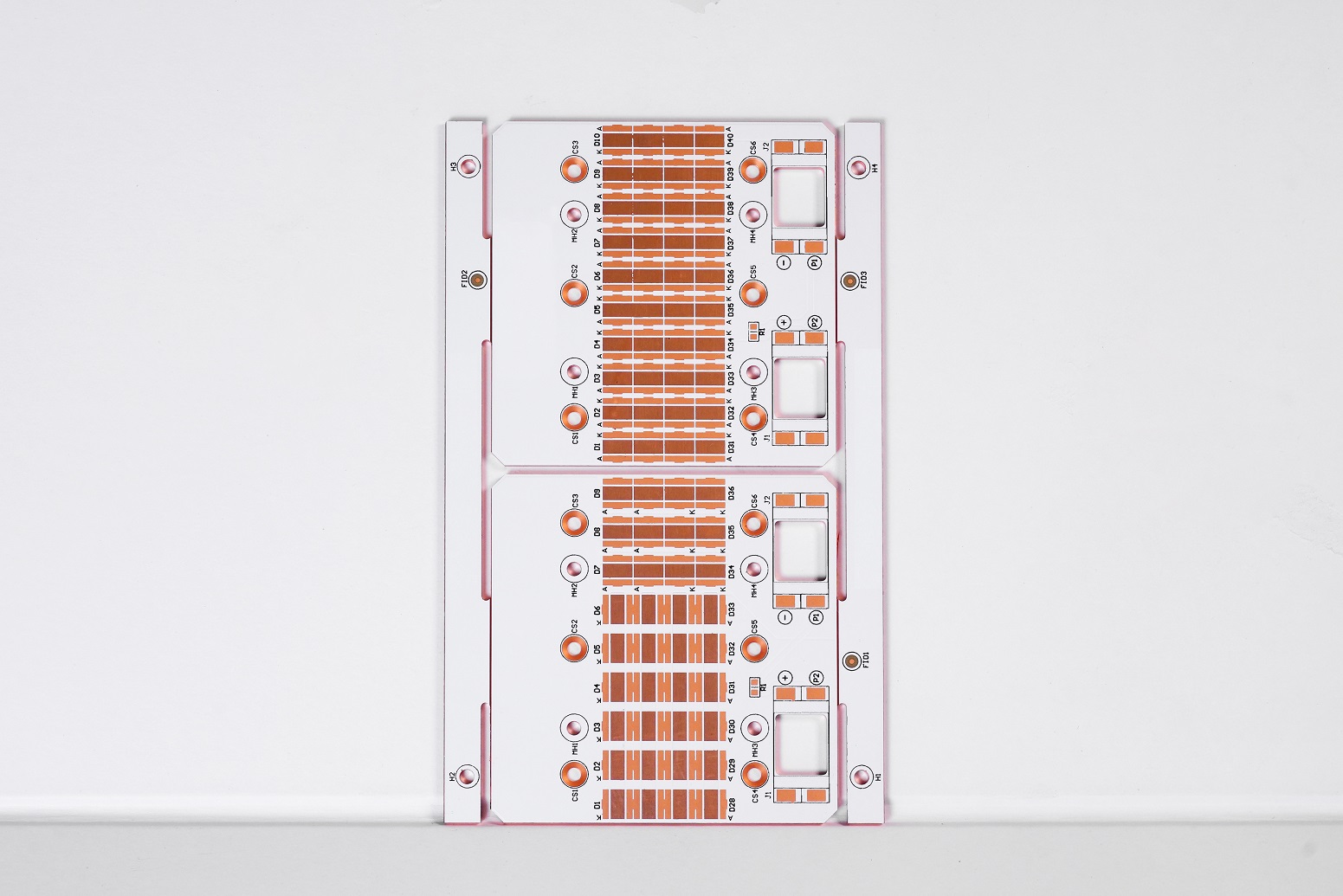
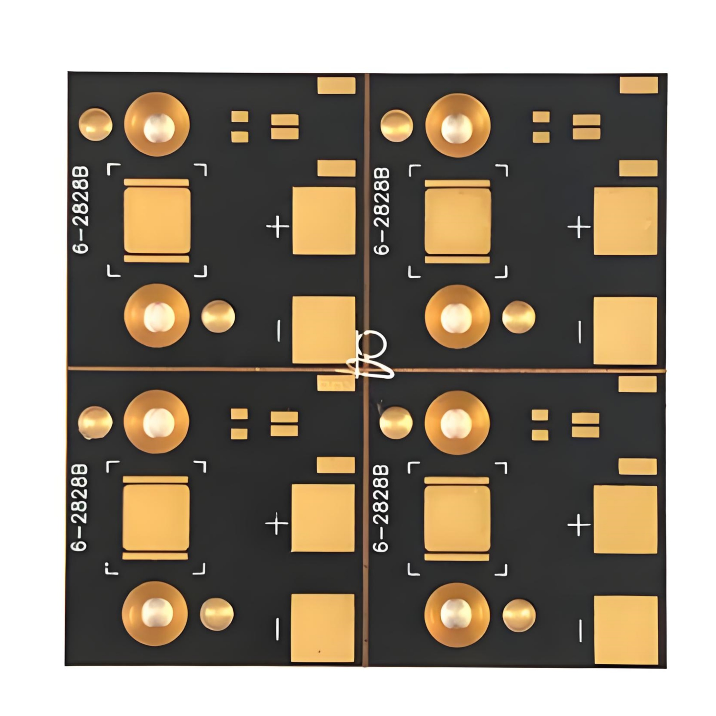
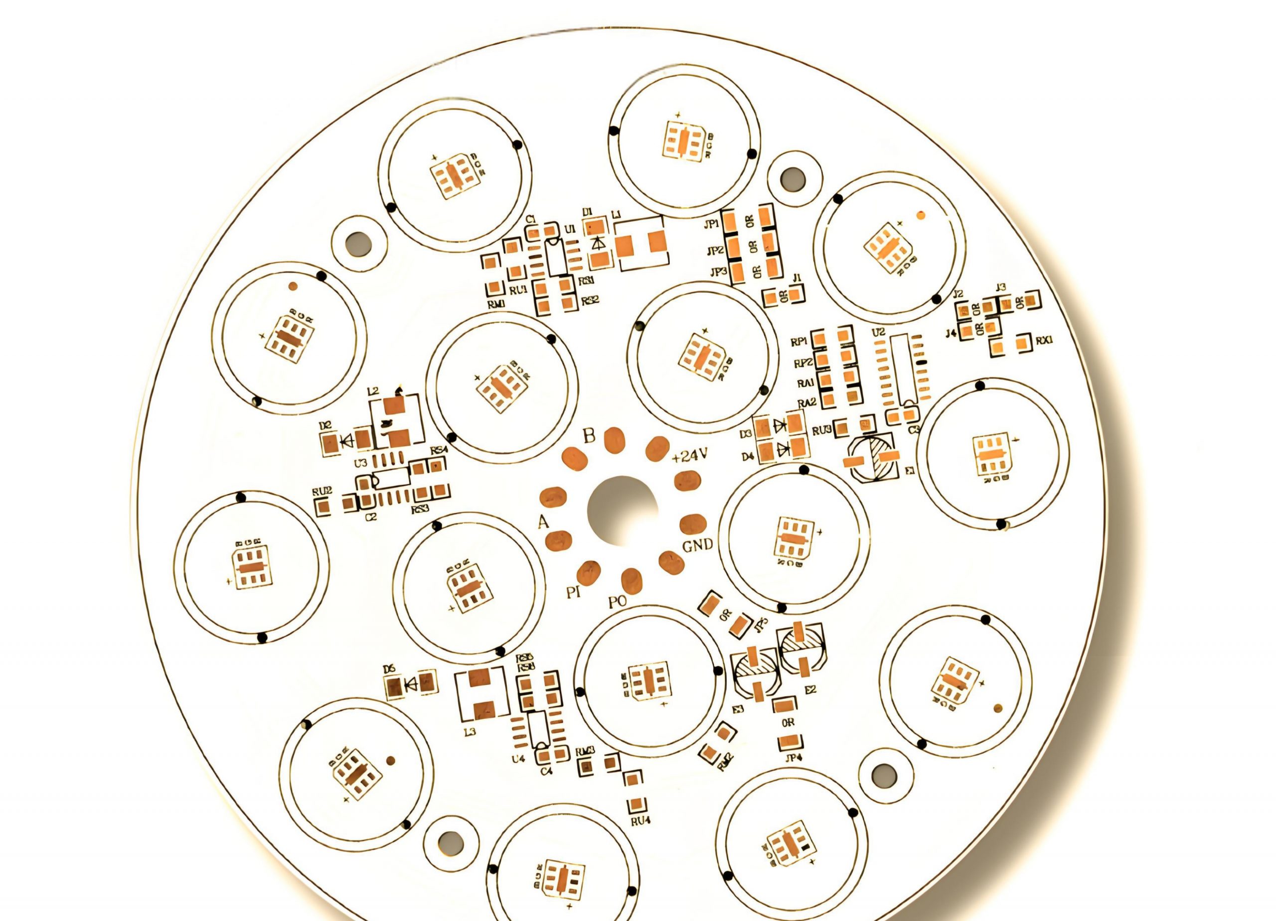
PCB manufacturing PCB manufacturing
Home > Blog

Direct Thermal Path Copper PCB Manufacturer

June 4th, 2025

What Is Direct Thermal Path Copper PCB?

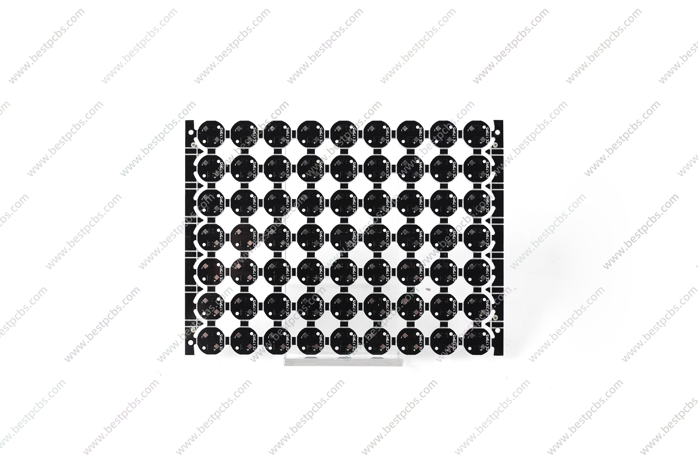
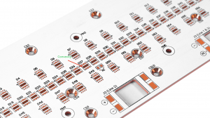
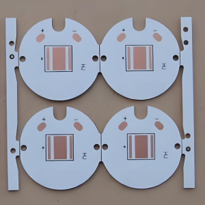
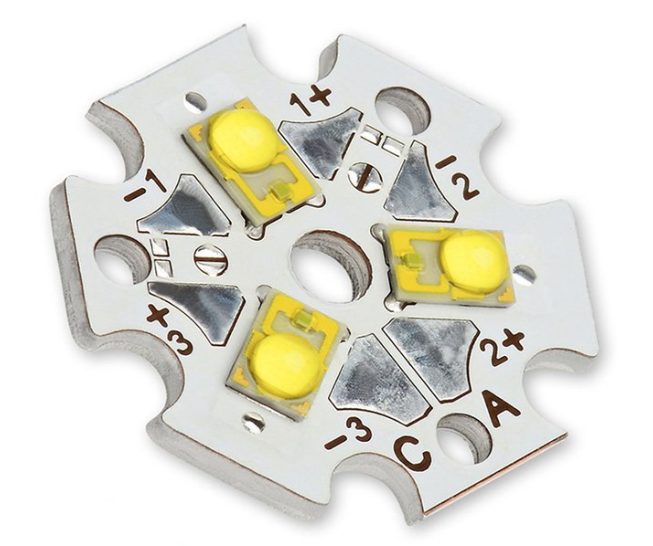
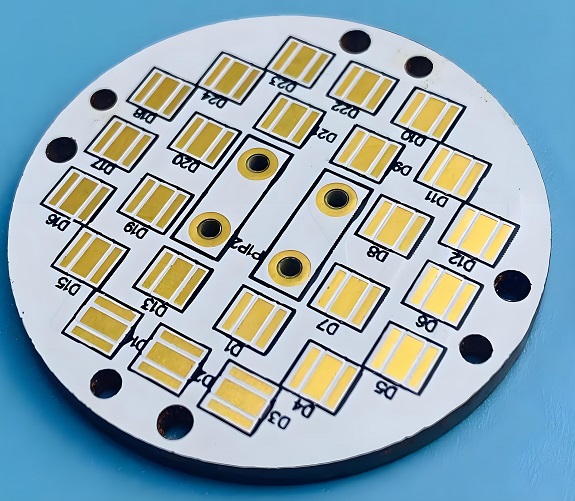
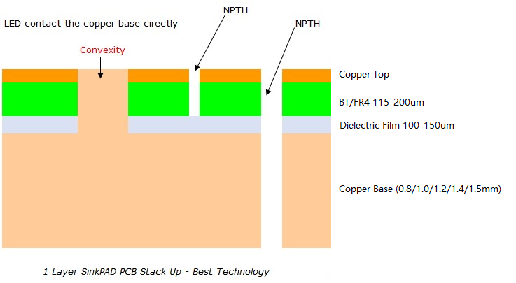
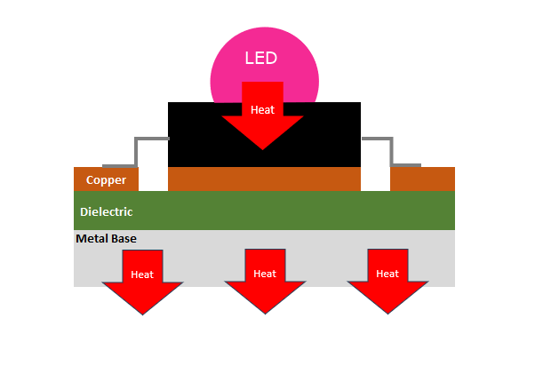
A Direct Thermal Path Copper PCB, also called DTP copper PCB or sinkpad copper base PCB. It is a type of high-performance circuit board used in applications where heat dissipation is critical. Unlike standard printed circuit boards (PCBs), which rely on dielectric layers to insulate the copper circuitry from the metal base, a DTP PCB removes this insulation layer directly beneath the heat-generating components. This creates a direct connection between the component, the copper layer, and the copper base.

This structure allows heat to flow quickly and efficiently away from the source, reducing thermal resistance and improving the performance and reliability of electronic components, especially in high-power or high-current environments. These boards are widely used in LED lighting, automotive systems, telecom infrastructure, and power electronics.
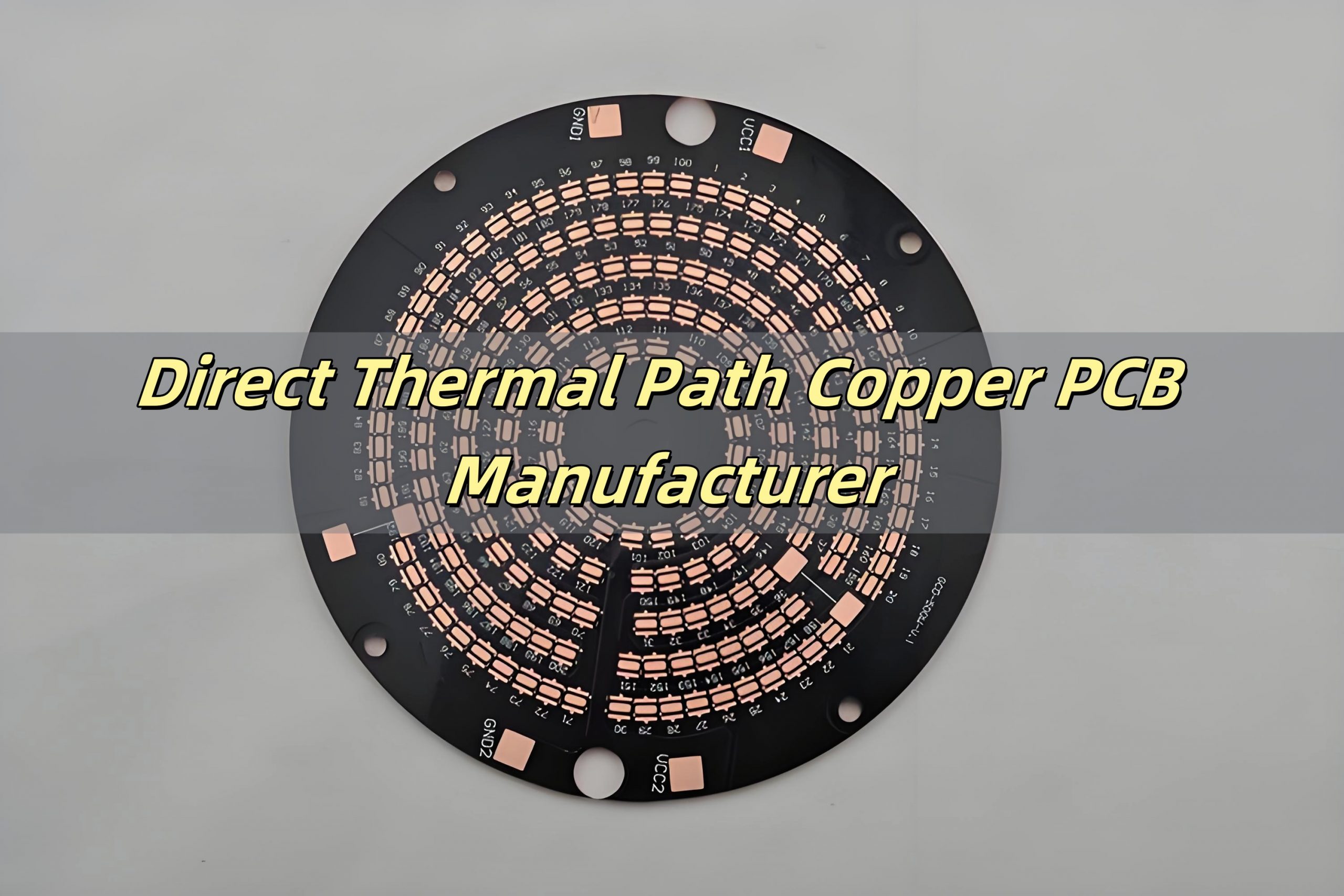
Direct Thermal Path Copper PCB Manufacturer

Why Thermal Management Matters in Electronics?

Every electronic device generates heat when it’s running. While small gadgets like phones may only get warm, high-power devices like industrial lighting systems or motor controllers can heat up rapidly. If this heat isn’t removed effectively, it can cause serious problems:

  • Component failure
  • Reduced lifespan of electronic parts
  • Malfunction due to overheating
  • Safety risks, especially in automotive or aerospace applications

To prevent these outcomes, thermal management becomes a critical aspect of PCB design. Engineers use a combination of heat sinks, thermal vias, and copper planes—but in extreme conditions, these are often not enough. That’s where DTP copper PCBs come in—they allow maximum heat transfer from hot components to the surrounding environment, helping electronics run cooler and more reliably.

Features of DTP Copper PCB

Direct thermal path copper PCBs stand out due to their special construction and capabilities. Here are some of their key features:

  • Thick copper base (up to 10 oz or more): Helps carry more current and draw heat away quickly.
  • Direct contact between copper circuit and metal base: Eliminates the thermal barrier of dielectric materials.
  • Excellent heat dissipation: Thermal resistance is significantly lower compared to regular MCPCBs.
  • Strong mechanical structure: Supports heavy components without deformation or cracking.
  • Stable performance in harsh environments: Suitable for high-temperature, vibration, and high-voltage conditions.

These features make DTP PCBs a practical choice for demanding applications where standard PCBs would overheat or fail.

How Does DTP PCB Work?

The principle behind a DTP PCB is simple: remove the thermal barrier (dielectric layer) between the heat source and the metal base. In a typical metal core PCB, the heat generated by a component passes through a dielectric layer (which is an electrical insulator) before reaching the metal base. This dielectric slows down the heat transfer.

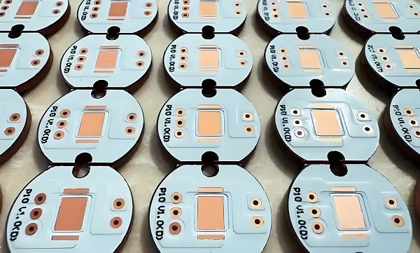
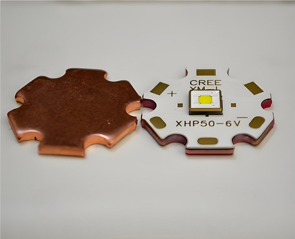
In a DTP PCB, the designer removes the dielectric material under the power component and creates a direct copper pad that touches the metal base directly. This structure dramatically reduces thermal resistance and allows heat to flow out much faster.

In short, DTP PCBs give heat a shortcut—a direct path to escape—leading to lower operating temperatures and better performance.

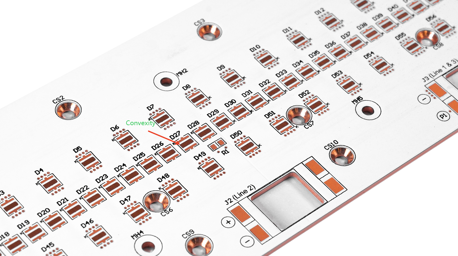
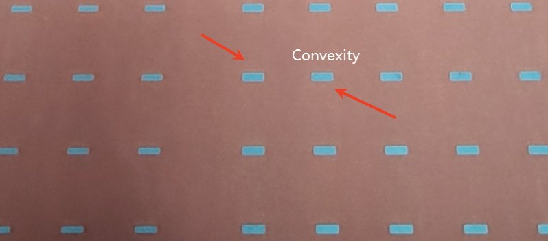
How Does the Convexity Pad Create?

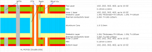
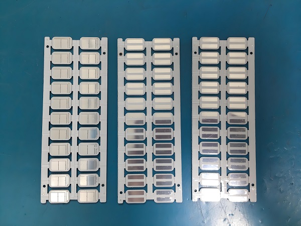
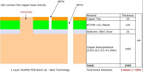
The convexity pad is a small bump or raised copper structure that connects the top copper circuitry directly to the metal base below. This feature is critical in DTP PCBs because it serves as the contact point for heat transfer. Actually, the convexity pad is a little complicated than normal. Normally the thickness of copper core/substrate is 0.8mm, 1.0mm, 1.2mm, 1.4mm, 1.6mm, 2.0mm. And there’re blue protection film on both sides. We will remove that protection film after raw material cutting, before convexity making, so that copper can be etched. After that, we will grind the copper core to make sure it’ll be clear enough, so that in next step another film can be added to make trace.

Then, we will add one extra layer of film (normally blue color, and will refer to blue film hereafter) on whole area copper core, and after developing & etching, only selected area of blue film will be kept and other area will be removed away. In fact, the area of blue film will be the place convexity will be.
Direct Thermal Path Copper PCB Manufacturer

Why Aluminum Base Is Not Suitable to Make DTP PCB?

As we know, the convexity pad directly connects the copper base serving as the substrate to the thermal pads of the LED without any insulating thermal conductive material in between. In this way, the heat from the LED can be directly transferred to the copper substrate of the base through the solder, without having to pass through the electrical traces on the base surface and the insulating materials for heat transfer. This is why DTP PCB also is called thermoelectric isolation as well. (The heat output path of the LED is directly connected to the copper plate and separated from the electrical traces). As for why aluminum substrates cannot be used, it is because the heat pads of the led chips need to be directly soldered to the copper substrate through the solder on the reserved protrusion on the base, and aluminum doesn’t bond well with standard solder materials.

In addition to this, some manufacturers said they can make DTP aluminum PCB. Maybe they indeed made it, but need to spend a lot of time and the cost is much higher than DTP copper base PCB. And compared with copper base PCB, the thermal conductivity of aluminum PCB is slightly lower, so we always not recommend customers to make DTP aluminum PCB.

Considerations While Using Direct Thermal Path MCPCB

Before incorporating DTP copper PCBs into your design, keep these factors in mind:

1. Component Placement

Ensure components that generate high heat are directly above the DTP pads. Misalignment can compromise thermal efficiency.

2. Base Thickness

The thickness of the copper base affects both heat transfer and mechanical strength. Heavier bases improve heat conduction but may reduce flexibility.

3. Thermal Simulation

Use thermal analysis software to simulate heat dissipation before production. This helps identify hotspots and optimize layout.

4. Dielectric Material

Where dielectric is still used, choose materials with high thermal conductivity (such as ceramic-filled polymers).

5. Mounting & Enclosure

DTP PCBs perform best when mounted to a heatsink or metal enclosure. Make sure there’s good thermal interface material between them.

6. Surface Finish

Use finishes like ENIG (Electroless Nickel Immersion Gold) or OSP (Organic Solderability Preservative) to improve soldering and surface protection.
Direct Thermal Path Copper PCB Manufacturer

DTP Copper PCB Manufacturing Process

Manufacturing a direct thermal path copper PCB requires careful attention and precision. Here’s a step-by-step breakdown:

Step 1: Base Metal Selection

A thick copper base (typically 1.6–3.2 mm) is chosen as the base layer. This base serves as the thermal sink for the entire board.

Step 2: Lamination

A high-thermal conductivity dielectric is laminated to the copper base. This is done only where insulation is needed.

Step 3: Circuit Layer Preparation

A copper foil (typically 1–3 oz) is applied on top. The PCB manufacturer then performs photolithography and etching to define the circuit pattern.

Step 4: Dielectric Removal

The dielectric under high-heat components is selectively milled or punched to expose the copper base.

Step 5: Convex Pad Formation

Using precision CNC machining, a raised copper pad is formed on the exposed area. This pad directly contacts the component’s thermal pad.

Step 6: Surface Finishing

The board receives a protective finish like ENIG, OSP, or immersion silver to prevent oxidation and improve solderability.

Step 7: Solder Mask and Silkscreen

Solder mask is applied to protect the circuitry, followed by silkscreen for labeling.

Step 8: Testing and Quality Control

Each board undergoes electrical and thermal testing to ensure performance, conductivity, and durability.

This manufacturing process results in a high-performance PCB that can handle extreme heat conditions with ease.

https://www.youtube.com/watch?v=KFQNdAvZGEA

Common Applications of DTP MCPCB

Because of their outstanding heat management, DTP copper PCBs are widely used across industries that rely on high-power or high-brightness components. Here are some key applications:

  • Automotive LED lighting: Headlights, brake lights, and DRLs require efficient thermal dissipation to maintain brightness and longevity.
  • Power electronics: DTP PCBs are used in DC/DC converters, motor controllers, and battery management systems for better heat control.
  • Industrial lighting: High bay and floodlights benefit from improved thermal design to prevent premature failure.
  • Telecommunication systems: Base stations and network equipment use DTP PCBs to manage heat from amplifiers and processors.
  • Aerospace and defense: Systems in satellites and aircraft need PCBs that perform reliably under thermal and environmental stress.

Wherever performance and reliability are non-negotiable, DTP copper PCBs are a trusted solution.

FAQs About Direct Thermal Path MCPCB

Q1. What makes DTP PCBs different from regular MCPCBs?

The key difference is the removal of the dielectric layer beneath the component, enabling direct heat flow from the copper pad to the metal base. This dramatically improves thermal conductivity.

Q2. Can DTP copper PCBs be used in multilayer stackups?

Typically, they are single-sided. However, hybrid multilayer configurations are possible for complex applications, though they require advanced design and manufacturing techniques.

Q3. Is copper the only metal used for DTP base material?

In high-end applications, copper is the preferred base due to its superior conductivity and durability. Aluminum is cheaper but less effective in DTP designs.

Q4. Do I still need a heatsink with a DTP PCB?

Yes, in most cases. While the DTP board efficiently moves heat to its base, the heat still needs to exit the board—often through a heatsink or the product’s metal housing.

Q5. How can I get a DTP copper PCB made?

You’ll need a PCB manufacturer like EBest Circuit (Best Technology) that specializes in metal core PCBs and has equipment for precision CNC milling and selective dielectric removal. Request thermal simulation support for best results.

You may also like

What is IMS PCB? IMS PCB Stack-up

June 4th, 2025

What is IMS PCB?

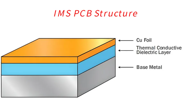
IMS PCB stands for Insulated Metal Substrate Printed Circuit Board. It’s a specialized type of PCB designed to manage heat more effectively than standard boards. At its core, an IMS board is made of three main layers: a metal base (usually aluminum), a thermally conductive dielectric layer, and a copper circuit layer on top.

This unique construction gives IMS boards exceptional heat transfer capabilities. Unlike standard FR4 boards, where heat may accumulate and degrade performance over time, an IMS PCB actively channels heat away from components and dissipates it through the metal base. This process helps protect sensitive parts and improves overall device longevity.

IMS PCBs are commonly used in LED lighting systems, power converters, automotive electronics, solar inverters, and industrial control systems. Any circuit that generates significant heat can benefit from the enhanced thermal management of an IMS PCB.

What is IMS PCB? IMS PCB Stack-up

Features of IMS PCB

IMS PCBs are favored in demanding applications because of their distinct advantages. Below are some of the standout features:

1. The dielectric layer in an IMS PCB has much higher thermal conductivity compared to FR4.

2. Once heat reaches the metal base, it is dispersed across a larger surface area or transferred to a heatsink.

3. The metal base not only helps with heat but also strengthens the board. This added rigidity reduces the chances of warping, especially in environments with temperature cycling or mechanical stress.

4. Components perform better and last longer when they remain within optimal temperature ranges.

5. Most IMS boards are single-sided, simplifying the layout and making them easier to manufacture. However, advanced designs may include multilayer configurations when required.

6. The metal base can also serve as a shield against EMI interference, which is useful in sensitive analog or RF applications.

Types of IMS Boards

Different IMS boards are used for different applications depending on the metal type and overall construction. Here are the three primary types:

  • Aluminum-Based IMS PCB

This is the most popular type and often the first choice for LED lighting and consumer electronics. Aluminum is lightweight, affordable, and has decent thermal performance. It strikes a balance between cost and functionality for a wide range of applications.

  • Copper-Based IMS PCB

Copper has better thermal and electrical conductivity than aluminum. These boards are used in high-end applications where superior thermal management is critical, such as power modules, solar inverters, and automotive control systems. However, copper is more expensive and heavier than aluminum.

  • Steel-Based IMS PCB

Less common but useful in environments where mechanical durability is crucial. Steel doesn’t conduct heat as efficiently as copper or aluminum but provides maximum rigidity and resistance to deformation. It’s mainly used in industrial or military electronics.

Each type of IMS PCB is selected based on the specific needs of your project. Aluminum offers a good starting point, copper pushes performance higher, and steel provides strength for the harshest conditions.

IMS PCB Stack-up

A critical element in IMS board design is the stack-up, which refers to how the different layers of the board are arranged. The typical IMS PCB stack-up includes the following:

IMS PCB Stack-up

1. Copper Layer

This is where all the electronic traces and pads are formed. The copper thickness usually ranges from 1 oz to 3 oz per square foot, depending on current requirements. It serves as the pathway for electrical signals and power.

2. Dielectric Layer

This is the thermally conductive but electrically insulating layer that separates the copper and the metal base. It’s usually made of a polymer filled with ceramic particles. The dielectric plays a vital role in transferring heat efficiently while preventing short circuits. The thickness typically ranges from 0.075 mm to 0.2 mm, with thermal conductivity from 1 to 7 W/m·K, depending on material grade.

3. Metal Base

This is typically made of aluminum, copper, or steel. The metal provides mechanical support and acts as the main heat dissipation path. Its thickness usually ranges from 1 mm to 2 mm, but thicker bases are used in heavy-duty applications.

Some advanced designs may include additional dielectric and copper layers to create double-layer or multilayer IMS PCBs, though this increases cost and complexity.

How Thick is an IMS PCB?

The total thickness of an IMS PCB is influenced by the materials used and application requirements. On average, the board thickness ranges from 0.8 mm to 3.2 mm, but custom configurations are available.

Here’s a breakdown of each layer’s contribution to overall thickness:

  • Copper Layer: 35–105 ”m (1–3 oz)
  • Dielectric Layer: 75–200 ”m
  • Metal Base Layer: 1.0–2.0 mm (for aluminum or copper)

Applications requiring high current typically demand thicker copper layers and sometimes thicker base metals. Likewise, if better insulation is needed, the dielectric layer can be made thicker, but this may reduce heat transfer efficiency. Engineers must balance electrical, thermal, and mechanical requirements to define the most suitable thickness.

How Thick is an IMS PCB?

What is the Difference Between IMS PCB and FR4 PCB?

Though both are used in electronic devices, the differences between IMS PCB and FR4 PCB are quite substantial:

ParameterIMS PCBFR4 PCB
Full NameInsulated Metal Substrate PCBFlame Retardant Grade 4 PCB
Base MaterialMetal core (usually aluminum or copper)Fiberglass-reinforced epoxy (FR4)
Thermal ConductivityHigh (1–7 W/m·K, depending on dielectric)Low (typically 0.3–0.4 W/m·K)
Heat DissipationExcellent, through metal baseLimited, requires heatsinks or fans
Layer StructureUsually single-sidedCan be single, double, or multilayer
Mechanical StrengthHigh (due to metal base)Moderate (flexible but less rigid)
WeightHeavier (due to metal core)Lighter
Manufacturing CostHigherLower
ApplicationsPower electronics, LEDs, automotive, solarConsumer electronics, IoT, communication devices
Thermal ResistanceLow (better heat flow)High (poor thermal path)
Electrical InsulationThrough thermally conductive dielectricProvided by FR4 material itself
Common Copper Thickness1–3 oz1–2 oz
Typical Board Thickness0.8–3.2 mm0.6–2.0 mm
Design ComplexityLower (usually single-layer)Higher (multilayer and complex routing possible)
Price RangeMid to HighLow to Mid

What is the Thermal Resistance of IMS Board?

Thermal resistance (Rξ) refers to a material’s resistance to heat flow. In IMS PCBs, it is mainly influenced by the dielectric layer. A lower Rξ means better heat transfer and lower temperature rise.

The thermal resistance of an IMS board is calculated using:

Rξ = t / (k × A)

Where:

t = dielectric thickness

k = thermal conductivity

A = surface area

Typical values for IMS PCBs range from 0.2°C/W to 1.0°C/W, depending on materials and layout. Advanced dielectric materials with high k-values can push this number lower, helping improve performance in high-power applications.

Designers often select materials with k ≄ 3 W/m·K and limit the dielectric layer to under 150 ”m to achieve low thermal resistance.

EBest Circuit (Best Technology) – Reliable IMS PCB Manufacturer

If you’re sourcing IMS PCBs and want consistent quality, EBest Circuit (Best Technology) is your go-to IMS PCB manufacturer. We have a dedicated production line for metal-core PCBs, including aluminum, copper, and hybrid metal boards.

Why Choose EBest Circuit (Best Technology)?

✅ Professional Engineering Support: Our experienced team helps optimize stackups, select dielectric materials, and improve thermal paths in your layout.

✅ ISO Certifications: We are certified with ISO9001, IATF16949, ISO13485, and AS9100D, serving a wide range of industries including medical, automotive, and aerospace.

✅ MES Traceability: Every board is tracked using our MES system to ensure complete traceability from raw materials to final shipment.

✅ Flexible Volumes: Whether you need a prototype batch or full-scale production, we offer scalable solutions.

✅ Comprehensive IMS PCB Assembly: Beyond PCB fabrication, we also offer full assembly including component sourcing, reflow soldering, inspection, and testing.

From concept to finished product, we work closely with clients to deliver high-performance IMS PCBs that meet electrical, mechanical, and thermal demands.

FAQs

1. What does IMS PCB stand for?

It stands for Insulated Metal Substrate Printed Circuit Board, a high-performance board for heat-sensitive applications.

2. Can IMS PCB be double-sided?

Yes, though less common. Double-sided IMS PCBs require more advanced fabrication and cost more, but they’re available for complex designs.

3. Is IMS PCB good for automotive systems?

Absolutely. Automotive systems generate a lot of heat and require reliability. IMS PCBs are ideal for ECUs, power converters, and headlight controls.

4. What thermal conductivity should I choose for my dielectric layer?

It depends on the heat generated. For moderate power, 1–2 W/m·K is enough. For high-power LEDs or power modules, choose ≄3 W/m·K.

5. How do I request a quote from EBest Circuit (Best Technology)?

Send your Gerber files, stackup requirements, and assembly needs to our team, and we’ll respond with a customized quote within 24 hours.

You may also like

Copper Core PCB vs Aluminum PCB: How to Choose the Right One? – Series 2

May 24th, 2025

In our last blog, we introduced the definition and basic of copper core PCB. But copper core PCB isn’t the only one metal core PCB, aluminum PCB provides good heat dissipation as well. So, when working with metal core boards, many engineers and buyers are unsure whether to choose an aluminum PCB or a copper core PCB. Some believe copper is always better, while others go with aluminum for lower cost. Today, we will guide you how to choose them, then let’s start it!

Material Comparison: Copper vs Aluminum Core

Both copper and aluminum are used as the core material for thermal management in PCBs, but their physical and electrical properties differ significantly:

PropertyCopperAluminum
Thermal Conductivity~380–400 W/m·K~200–230 W/m·K
Electrical Conductivity~58 MS/m~35 MS/m
Density8.96 g/cmÂł2.70 g/cmÂł
StrengthHigher rigidityMore flexible
Cost1.5x to 3x higherLower

Copper provides superior conductivity and better rigidity but comes at a much higher cost and weight. Aluminum is lighter, easier to machine, and cost-effective for mid-range applications.

Thermal Management: Which One Handles Heat Better?

When heat dissipation is your top priority, copper clearly wins. Its high thermal conductivity allows heat to spread faster and more evenly, which is critical in high-power applications like:

  • LED floodlights and stadium lighting
  • Automotive headlights
  • Power converters and inverters
  • Laser driver modules

Case example: A customer replaced an aluminum PCB with a copper base for a 100W LED driver. The operating temperature dropped by 15°C, drastically improving product lifespan.

However, in low-to-mid power systems—like ceiling lights, LED bulbs, or camera light rings—aluminum is typically sufficient. Using copper in these cases is often unnecessary and drives up costs without clear benefits.

Mechanical Strength and Weight: What Does Your Design Need?

Copper core PCBs are heavier and more rigid, which makes them better for industrial applications exposed to vibration or extreme temperature cycles.

But in products where weight matters—like drones or wearable devices—aluminum PCBs are the smarter option. They are easier to machine, route, and assemble. They also cost less in terms of tooling and manufacturing time.

Choose copper core PCBs if you need:

  • High mechanical stability
  • Vibration resistance
  • Long-term thermal durability

Choose aluminum PCBs if your product needs:

  • Lightweight design
  • Cost control
  • Simpler routing and drilling

Cost Consideration: Is Copper Always Worth It?

Let’s be honest: copper core PCBs can cost up to 3x more than aluminum PCBs. So you should ask yourself—is the higher thermal performance really necessary for your design?

Aluminum PCBs are the better choice when:

  • Your application doesn’t exceed 80W–100W
  • Weight and cost are design priorities
  • You’re in mass production and need price stability

Copper core PCBs are justified when:

  • Your system needs to handle heavy heat loads
  • High current density is involved
  • Long-term reliability matters more than price

Many of our customers reduce total project cost by switching to aluminum PCBs without sacrificing performance—once we review their thermal simulation data.

Where to Use Each PCB Type?

Here’s a quick-reference table to match your application with the recommended base material:

ApplicationRecommended BaseReason
High-power LED floodlightsCopperHeat and current requirements are high
Automotive lighting systemsCopper or thick aluminumPerformance and safety critical
Indoor LED lightingAluminumLower heat, cost-sensitive
Power modules & invertersCopperHigh voltage and thermal stress
Camera flash or ring lightAluminumLightweight and cost-friendly
Medical power supplyCopperStability and safety required
LED floodlights (150W+)Copper Core PCBHandles heat better
LED bulbs & home lightingAluminum PCBAffordable and thermally sufficient
EV chargers & power modulesCopper Core PCBHigh reliability under load
Camera flashes & portable lightsAluminum PCBLightweight and budget-friendly
Medical devices (power control)Copper Core PCBPrecise, stable performance
Consumer electronicsAluminum PCBCost-efficient for large volumes

Use this guide to avoid over-engineering or under-specifying your metal core PCB.

5 Key Points Before You Choose

Still not sure which base material fits your needs? Walk through this five-step checklist:

1. Power Level: How much current and heat does your circuit handle?

2. Installation Environment: Is weight a constraint? Will it face vibration?

3. Target Cost: Are you selling a premium or mass-market product?

4. Design Complexity: Do you need tight tolerances or complex routing?

5. Volume & Lead Time: Can your supplier meet deadlines for the material?

If you answered “high” for performance on most points, copper is likely the way to go. If not, aluminum is your best cost-performance choice. By the way, if you’re unsure after answering these, consult with your PCB manufacturer. At EBest Circuit (Best Technology), we provide application-based advice to help you choose between aluminum PCBs and copper core PCBs—without overspending.

Why Choose EBest Circuit (Best Technology) for Your Metal Core PCB?

Whether you need aluminum base PCBs for standard lighting or copper base PCBs for high-power industrial applications, EBest Circuit (Best Technology) has you covered:

  • Mature production lines for both copper and aluminum base PCBs
  • One-on-one design support, thermal simulation, and DFM reviews
  • Full in-house capabilities: thick copper etching, CNC routing, V-cutting
  • Fast sample turnaround and stable mass production support
  • Strict quality control and traceability through MES system
  • Expert engineering team for application-specific advice

Reach out to EBest Circuit (Best Technology)—we’ll help you analyze your application, recommend the ideal PCB solution, and even support custom development if needed.

FAQs

Q1: Can I use aluminum base PCBs for high-power applications?

Only for moderate heat loads. For >100W power systems, copper is strongly recommended.

Q2: What is the thinnest aluminum or copper base you can provide?

We can produce down to 0.8mm base thickness for both, depending on the structure.

Q3: Do you offer hybrid metal core PCBs?

Yes, we can integrate aluminum and FR4 or support copper-ceramic hybrid designs.

Q4: How long is the lead time for copper vs aluminum base?

Aluminum PCBs: 5–7 working days; Copper PCBs: 7–12 days depending on complexity.

Q5: Can I get thermal simulation before placing an order?

Absolutely! We offer pre-production thermal analysis and structural design assistance.

Q6: Are copper core PCBs compatible with standard SMT processes?

Yes, they are. We offer full SMT assembly services for both aluminum and copper base boards.

Q7: How do I know which type is best for my application?

Send us your design or specs, and we’ll recommend the most cost-effective and reliable option.

Conclusion

Choosing between a copper core PCB and an aluminum PCB isn’t about choosing the better material. It’s about selecting what’s right for your application. Copper is powerful but expensive; aluminum is flexible and affordable.

When designed and selected correctly, aluminum PCBs can outperform expectations, and copper core PCBs can save your system from thermal failure. Match the material to your environment, budget, and performance goals—and you’ll never go wrong. In our next blog, we will share how to select the thickness of copper. If you are interested in it, collect us and keep reading.

You may also like

Custom PCB Sinkpad for High-power LED Solutions

May 23rd, 2025

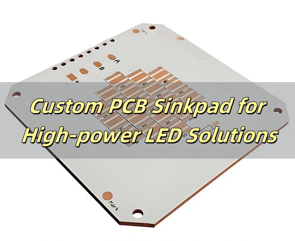
High-power LED applications come with a serious challenge: heat. When LEDs generate too much heat and it’s not properly managed, it can shorten the life of the light, affect its brightness, or even cause total failure. That’s where SinkPAD PCBs come in. Unlike regular MCPCBs, a SinkPAD PCB offers a direct thermal path that transfers heat away from the LED quickly and effectively. If you’re working with powerful LEDs, custom SinkPAD PCBs can make a big difference. At EBest Circuit (Best Technology), we specialize in custom SinkPAD solutions designed for maximum heat dissipation and long-term reliability.

What is a SinkPAD PCB and How Does it Work?

A SinkPAD PCB is a type of metal core PCB designed specifically for high-thermal performance. The term “SinkPAD” refers to a patented technology where the thermal pad of the LED is directly connected to the metal base of the PCB, creating an uninterrupted thermal path. In traditional MCPCBs, a dielectric layer sits between the copper circuit layer and the metal base, reducing thermal conductivity. But in a SinkPAD design, that barrier is removed or minimized in the area under the LED, allowing heat to flow directly to the metal core and then to the heatsink.

Custom PCB Sinkpad for High-power LED Solutions

Why is Thermal Management So Critical in High-Power LED Applications?

LEDs are efficient, but they’re not immune to heat. In fact, around 70%–85% of the electrical energy in an LED is converted into heat. If that heat isn’t quickly removed, it can cause several issues:

  • Decreased light output (lumen depreciation)
  • Color shifting over time
  • Shorter lifespan
  • Component failure in extreme cases

Good thermal management maintains LED brightness, performance, and stability. For high-power LEDs, such as those used in automotive headlights or industrial lighting, standard cooling methods often fall short. That’s why advanced thermal solutions like custom SinkPAD PCBs are essential — they offer superior heat dissipation to keep your LEDs working reliably.

What are the Advantages of Custom SinkPAD PCBs for LED Projects?

Choosing a custom SinkPAD PCB means tailoring the thermal design to fit your exact LED setup. Here are the key benefits:

  • Better heat dissipation: The direct thermal path lowers the junction temperature, which helps maintain brightness and prevent overheating.
  • Compact design: You can eliminate bulky heatsinks, which saves space in your lighting product.
  • Improved reliability: Lower operating temperatures lead to fewer failures and longer LED lifespan.
  • Higher power density: You can run brighter or more LEDs in a small area without worrying about thermal overload.
  • Consistent performance: No hotspots or uneven heat spread — just stable and predictable operation.

A custom SinkPAD solution allows you to match the board layout, materials, and thickness exactly to your LED requirements, which is especially helpful for complex or high-end lighting systems.

Custom PCB Sinkpad for High-power LED Solutions

What Materials are used in SinkPAD LED PCBs?

The choice of materials is crucial for any high-performance PCB, especially one handling thermal management. In SinkPAD PCBs, the most common materials include:

  • Aluminum base: Widely used due to its cost-effectiveness and good thermal conductivity. Suitable for medium-power LED applications.
  • Copper base: Offers superior heat conductivity compared to aluminum and is typically used in ultra-high-power or demanding environments.
  • High-thermal conductivity dielectric (if used): In areas not using the exposed metal pad, a thin dielectric layer may still be present. The goal is to keep thermal resistance as low as possible.

At EBest Circuit (Best Technology), we work with both aluminum and copper bases and can advise on the best choice depending on your heat requirements and budget.

How is a SinkPAD PCB Manufactured?

The SinkPAD PCB manufacturing process requires high precision and special techniques to expose the thermal pad directly to the metal base. Here’s how it typically works:

  1. Material preparation: Selection of copper or aluminum core with appropriate thickness.
  2. Drilling and routing: Laser or mechanical drilling is used to create openings that allow the thermal pad to contact the base metal directly.
  3. Etching and circuit formation: Copper traces are etched for the electrical circuit.
  4. Thermal pad exposure: Dielectric material is selectively removed from under the LED thermal pad area.
  5. Plating and finishing: Surface finishes like ENIG or OSP are applied to the copper pads.
  6. Testing and inspection: Thermal and electrical tests ensure the board performs as intended.

This process allows the heat from the LED to travel through the exposed pad directly into the metal base, rather than relying on thermal via stacking or thick dielectric layers.

Where are SinkPAD PCBs Used in Real Applications?

SinkPAD PCBs are used in any application where high power and reliable thermal control are required. Here are some real-world examples:

  • Automotive headlights and fog lamps: Require compact designs and powerful light with efficient heat dissipation.
  • Industrial floodlights: Often run for long hours and need stable performance under high thermal stress.
  • Medical lighting: Such as surgical lights that demand high brightness and zero failure during operation.
  • UV curing systems: Used in printing and adhesives, which generate intense heat.
  • Stage or studio lighting: Where color consistency and brightness are key, and high-powered LEDs are standard.

These applications benefit from the direct thermal pathway offered by SinkPAD PCBs, ensuring the LEDs can operate at full brightness for long periods without failure.

Design Considerations of SinkPAD PCB in LED Lighting Devices

When designing a SinkPAD PCB for LED lighting, it’s not just about efficient heat dissipation — it’s about optimizing performance, reliability, and manufacturability. Here are the key factors to consider:

1. LED Thermal Pad Alignment

Ensure the thermal pad of the LED package aligns precisely with the exposed metal area of the SinkPAD. Any misalignment can increase thermal resistance and reduce heat transfer efficiency.

2. Base Metal Selection

Aluminum is cost-effective and sufficient for many applications, but copper is preferable for ultra-high-power LEDs due to its superior thermal conductivity. Choose the base metal based on your LED’s power output and operating environment.

3. Board Thickness

The thickness of the metal core affects both heat spreading and mechanical strength. Thicker cores (e.g., 2.0mm copper or aluminum) can handle more heat but may increase the overall weight and cost.

4. Dielectric Isolation (If Applicable)

In areas that don’t require direct heat transfer, a thin dielectric layer may still be used. Select materials with high thermal conductivity (>1.0 W/m·K) and low thermal resistance to maintain performance.

5. Surface Finish

For high-reliability soldering and corrosion resistance, finishes like ENIG (Electroless Nickel Immersion Gold) or OSP (Organic Solderability Preservative) are commonly used. Choose a finish compatible with your LED’s soldering profile.

6. Component Layout and Spacing

Leave enough space between LEDs and other heat-sensitive components. This helps prevent local hotspots and ensures even heat distribution across the board.

How Does EBest Circuit (Best Technology) Serve You for Custom SinkPAD PCBs?

Choosing the right SinkPAD PCB partner is as important as the design itself. Here’s how EBest Circuit (Best Technology) supports you at every step:

  • Advanced thermal engineering support
  • Material flexibility including copper and aluminum
  • Custom layout design
  • Certified quality system
  • Full traceability
  • Fast quoting and prototyping

With over a decade of experience in custom thermal PCB design, EBest Circuit (Best Technology) is your reliable partner for SinkPAD LED solutions.

FAQs

1. What’s the difference between SinkPAD and standard MCPCBs?

Standard MCPCBs use a dielectric layer between the LED and the metal core, while SinkPAD removes that layer under the thermal pad for direct heat transfer.

2. Can SinkPAD PCBs handle very high-wattage LEDs like 10W or 50W?

Yes. SinkPAD PCBs are specifically designed for high-wattage LEDs where rapid and efficient heat dissipation is critical.

3. Is copper better than aluminum for SinkPAD PCBs?

Copper offers better thermal conductivity than aluminum, but it’s also more expensive. The choice depends on your application and thermal budget.

4. Are SinkPAD PCBs only used for LED lighting?

While they’re most commonly used in LED applications, they can be used in any high-power electronics needing excellent thermal control.

5. How can I get a quote for a custom SinkPAD PCB?

Simply send us your Gerber files and project details. Our engineering and sales team will respond with a tailored solution and quotation within 24 hours.

You may also like

How Does the Cost of Sinkpad MCPCB Compare to Conventional MCPCB?

May 22nd, 2025

What Is Sinkpad MCPCB?

SinkPAD MCPCB is a special kind of metal core printed circuit board designed for excellent heat dissipation. It’s different from regular MCPCBs because it removes one major barrier—the insulating dielectric layer under the LED.

In simple terms, it allows heat to flow directly from the LED chip to the metal base. That means less heat build-up, more efficiency, and longer lifespan for your components.

You’ll often find SinkPAD MCPCBs in high-power LED applications—like automotive lighting, industrial lamps, medical equipment, and even UV curing systems. These are places where heat control isn’t just helpful—it’s essential.

What Is Sinkpad MCPCB?

Advantages of Sinkpad MCPCB

1. Direct Heat Flow

With no dielectric between the LED and metal core, SinkPAD boards offer a direct thermal path, reducing resistance and increasing efficiency.

2. Lower Operating Temperatures

By improving heat transfer, components stay cooler. For LEDs, this means stable brightness and a longer working life.

3. Consistent Light Output

Temperature spikes can dim or discolor LEDs. SinkPAD keeps the junction temperature stable, maintaining consistent color and brightness.

4. Compact Design

Thanks to better heat handling, you can reduce or eliminate bulky heatsinks, helping make designs smaller and lighter.

5. Durability in Harsh Conditions

SinkPAD boards resist thermal cycling, shock, and vibration, making them perfect for tough environments like aerospace or outdoor lighting.

So if your design involves powerful LEDs or components that get hot fast, this type of board can be a game-changer.

Base Materials of Sinkpad MCPCB

SinkPAD boards come with different base metals. Each one has its own strengths depending on your project.

  • Aluminum Core Sinkpad PCB

Aluminum is the more common choice. It’s lightweight, easy to work with, and keeps costs low. Its thermal conductivity is good—usually around 150-200 W/m·K. For applications where heat output isn’t extreme, aluminum SinkPAD PCBs are a great fit. You’ll find them in general LED lighting, backlit signs, and other consumer electronics.

They’re also a smart option if you’re trying to keep your SinkPAD MCPCB price in check. But actually, for consumer electronics, conventional metal core PCB can cover it.

Aluminum Core Sinkpad PCB
  • Copper Core Sinkpad PCB

Copper is all about performance. It has much higher thermal conductivity—around 385-400 W/m·K—which means it can handle intense heat. If your LEDs are pushing a lot of power or operating in a hot environment, copper is the better option. Some industrial like UV lights, high-performance lasers, or automotive headlights that stay on for long hours.

Copper Core Sinkpad PCB

Copper boards are heavier and more expensive than aluminum ones, but they deliver top-tier thermal results.
How Does Sinkpad MCPCB Work?

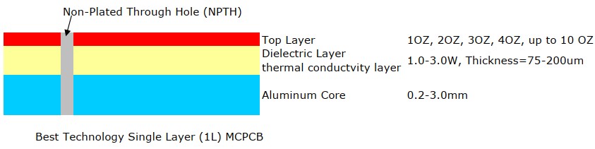
In a standard MCPCB, the LED sits on a copper trace. Under that trace is a dielectric layer. Below that is the metal core, its structure just like below. Heat has to travel through all of this to get out. That creates resistance.

How Does Sinkpad MCPCB Work?

However, sinkPAD skips the dielectric layer—at least under the LED’s thermal pad. Instead, the heat flows straight from the LED’s thermal pad into a thermal cavity that connects directly to the base metal. This structure is often called a Direct Thermal Path (DTP).

How Does Sinkpad MCPCB Work?

It’s like giving heat a shortcut out of the system. No extra layers. No slowdowns. Just fast, efficient cooling. This design improves overall thermal conductivity and gives you tighter control over junction temperatures.

Thermal Conductivity of Sinkpad MCPCB

Thermal conductivity is key when you’re dealing with LEDs and power electronics. The better the board can spread heat, the better your device performs.

With aluminum cores, you’ll typically see thermal conductivity in the 150–200 W/m·K range. That’s solid for most LED needs. With copper cores, you’ll reach up to 400 W/m·K, giving you elite heat handling.

Sinkpad MCPCB vs. Conventional MCPCB

So what are the differences between sinkpad metal core PCB and traditional metal core PCB? Here we made a comparison between them:

PropertySinkPAD MCPCBConventional MCPCB
Heat TransferDirect path (through convexity pad)Through dielectric
Thermal conductivityUp to 400W/m.kUp to 8W/m.k
Thermal Resistance0.4°C/W or lower1.0–2.0°C/W
Light StabilityHigh (because most use copper)Medium
LED LifespanExtendedShorter under heat
Space NeededNoLarger cooling required
CostSlightly higherLower upfront

SinkPAD boards give better performance and better results—especially when heat control is non-negotiable. They cost more, but what you get in return is worth it in critical applications.

Considerations When Using Sinkpad MCPCB

SinkPAD MCPCBs aren’t plug-and-play for every project. There are a few things you’ll want to keep in mind before designing with them.

1. Know Your Heat Load

If your LEDs don’t generate much heat, you might not need SinkPAD. But if your design involves high wattage, tight spaces, or long run times—then yes, it’s worth considering.

2. Choose the Right Core

Use aluminum if your budget is tight or if weight is a concern. Go with copper when you need every ounce of thermal performance you can get.

3. Plan for Heatsinks

Even though the board transfers heat well, it still needs a place to send that heat. Match your SinkPAD PCB with a proper heatsink or thermal interface.

4. Soldering Profiles

Because these boards transfer heat so quickly, your reflow or wave soldering profile might need to be adjusted. Too much heat too fast can be a problem.

5. Work With an Experienced Supplier

Not all board suppliers are familiar with SinkPAD technology. Make sure your manufacturer knows how to handle the convexity design and machining process correctly. If you are searching for a reliable sinkpad MCPCB manufacturer, do not miss out EBest Circuit (Best Technology). We have over 18 years experiences, and we have experienced engineers and operators to give you a high quality sinkpad copper core PCB.

How Does the Cost of Sinkpad MCPCB Compare to Conventional MCPCB?

So, how does the cost of sinkpad MCPCB compare to the conventional MCPCB? Actually, the price of sinkpad PCB is higher than that of a standard MCPCB. Because the process is more complex. There’s more precision involved in removing the dielectric under the LED. And if you’re using copper, that adds more to the cost.

Here’s what influences the price:

  • Core material (aluminum vs. copper)
  • Board size and thickness
  • Layer count
  • Volume of your order
  • Custom thermal pad design

But here’s the real question: does it save you money in the long run? For many, the answer is yes. Here’s why:

  • You don’t need oversized heatsinks
  • Your LEDs last longer
  • Fewer failures mean lower service costs
  • Your product performs better, with fewer returns

When you weigh the total system cost—not just the board—the extra investment often pays off.

SinkPAD MCPCBs offer a smart solution for thermal challenges in LED and power electronics. They bring something special to the table—direct heat transfer from the source to the metal base.

If your design involves strong heat loads, tight spaces, or critical reliability, this is the kind of PCB that can make a difference. In our next blog, we will share the factors affect the cost of sinkpad PCB. If you want to know more about sinkpad PCB, you are welcome to contact us at any time.

FAQs

1. What makes Sinkpad MCPCB more effective than a standard MCPCB?

    It creates a direct path from the LED to the metal core, removing the thermal barrier and increasing heat flow.

    2. Can I use aluminum Sinkpad MCPCB for high-power LEDs?

    Yes, if thermal output is moderate. For extreme power or heat, copper may perform better.

    3. Does it support double-layer designs?

    Sinkpad technology is usually single-sided due to its thermal cavity, but custom options are available.

    4. Is the cost justified in consumer products?

    In mid- to high-end products where longevity and brightness matter, yes. It reduces long-term failures and service needs.

    5. How do I choose between aluminum and copper Sinkpad cores?

    Look at the application. If weight and cost are more critical, aluminum works well. For demanding environments, copper is better.

    You may also like

    5 Factors Affect the Price of Sinkpad PCB

    May 20th, 2025

    What is Sinkpad Copper Based PCB?

    A sinkpad copper based PCB, also known as SinkPAD board or thermoelectric copper separation copper based PCB, is a specialized type of metal core printed circuit board. It mainly consists of two major parts: the top trace layer and the copper core/substrate. The top trace layer contains the electrical traces for the circuit, while the copper core serves as a heatsink.

    A 1 – Layer SinkPAD board, a common type, consists of a copper circuit layer, a dielectric (non – conducting) layer, and a metal core/pedestal which is usually copper. It belongs to single – sided SinkPAD PCB and DTP (Direct Thermal Path) board, and is the most popular and cost – effective stack – up option with the fastest lead time.

    Sinkpad Copper Based PCB: Everything You Need to Know

    Why Use Sinkpad Copper Based PCB?

    Sinkpad copper based PCBs are used for several important reasons. After lamination, the electronics connection is on the trace layer, and the direct thermal conducting PAD comes from the copper core. The trace PAD on the trace layer is in the sink area of the copper core, which gives it the name “SinkPAD board”. This design allows for efficient thermoelectric separation.

    These PCBs can reach a thermal conductivity of 400W/m.K. This high thermal conductivity is crucial in applications where heat dissipation is a major concern, such as in high – power LED lighting, power electronics, and other electronic devices that generate a significant amount of heat. By effectively dissipating heat, sinkpad copper based PCBs can improve the performance and reliability of electronic components and extend their lifespan.

    Factors Affect the Price of Sinkpad MCPCB

    • Material type (aluminum vs. copper)

    The choice of material has a significant impact on the price of sinkpad MCPCB. Copper is generally more expensive than aluminum. Copper has excellent thermal conductivity, which is one of the key advantages for sinkpad PCBs as it helps in better heat dissipation. However, the higher cost of copper raw materials and the more complex processing requirements contribute to the increased price.

    Aluminum, on the other hand, is a more cost – effective option. It has relatively good thermal conductivity and is lighter in weight. But its thermal performance is not as good as copper. When the application requires high – end thermal performance, copper is often the preferred choice, but it comes at a higher price.

    Sinkpad Copper Based PCB: Everything You Need to Know
    • Board size and thickness

    The size and thickness of the sinkpad copper based PCB also play a role in determining the price. Larger boards require more raw materials, such as copper and dielectric materials. Additionally, the manufacturing process for larger boards may be more complex, as it requires more precise alignment and processing steps.

    Thicker boards also add to the cost. Thicker copper cores or additional layers of materials increase the material cost. Moreover, thicker boards may require more advanced manufacturing techniques to ensure proper electrical and thermal performance, which can drive up the production cost.

    • Layer structure

    The layer structure of the sinkpad PCB is another important factor. A more complex layer structure, such as multi – layer sinkpad PCBs, is more expensive than single – layer ones. Multi – layer PCBs require more manufacturing steps, including additional lamination processes, drilling for vias to connect different layers, and more precise alignment of the layers.

    Each additional layer adds to the complexity and cost of the manufacturing process. For example, a 1 – Layer SinkPAD board is the simplest and most cost – effective option, while a PCB with multiple trace layers and copper core layers will be significantly more expensive.

    • Order quantity

    Order quantity has a direct impact on the price of sinkpad copper based PCBs. When the order quantity is large, the per – unit cost usually decreases. This is because manufacturers can take advantage of economies of scale. They can purchase raw materials in bulk at a lower cost, optimize their production processes, and reduce setup costs per unit.

    For small – quantity orders, the fixed costs associated with setting up the production line, such as tooling costs and programming costs, are spread over a smaller number of units. As a result, the per – unit price is higher. So, customers who need a large number of sinkpad PCBs can often negotiate a better price per unit.

    • Custom thermal pad design

    Custom thermal pad designs can also increase the price of sinkpad copper based PCBs. Standard thermal pad designs are more cost – effective because they can be produced using existing manufacturing processes and tools. However, if a customer requires a custom thermal pad design, it may involve additional engineering work, such as designing new masks, adjusting the manufacturing process, and conducting additional testing.

    Sinkpad Copper Based PCB: Everything You Need to Know

    Custom designs may also require special materials or manufacturing techniques to meet the specific thermal requirements. All these additional steps and requirements add to the overall cost of the PCB.

    Sinkpad Copper Based PCB Applications

    Sinkpad copper based PCBs have several common uses in the electronics industry:

    • Thermoelectric separation applications:

    Since the trace layer of SinkPAD boards is usually on the top side, they belong to single – sided SinkPAD PCBs and Direct Thermal Path (DTP) boards. This makes them suitable for applications where thermoelectric separation is required. For example, the SinkPad board provides excellent heat transfer from the LED to the base metal (copper) plate while maintaining excellent electrical isolation.

    • High – power LED applications:

    1 – Layer copper base SinkPad PCB: It can be used with surface mount and chip & wire components. The thermal PAD of the LED touches the convexity of the copper core/pedestal directly, achieving a thermal conductivity of 400W/m.K. The pad of the LED touches the copper base directly, allowing the heat generated by the LED to be dissipated quickly into the air or a heatsink, achieving the best heat dissipation and conduction.

    2 – Layers copper base SinkPad PCB: It can also be used with surface mount and chip & wire components. Similar to the 1 – layer version, the thermal PAD of the LED touches the convexity of the copper core/pedestal directly, with a thermal conductivity of 400W/m.K.

    In general, sinkpad copper based PCBs are used to provide superior thermal performance for medium – to high – power LEDs and other chips/components.

    How Does A SinkPAD board Differ From A Traditional PCB?

    A SinkPAD board is a special type of metal core PCB. In a SinkPAD board, the thermal conductive PAD is the convexity area of the copper core/pedestal, allowing the thermal PAD of the LED to touch the convexity area of the metal core directly. This enables the heat of the LED to be dissipated into the air much faster and more efficiently than a conventional PCB.

    The SinkPad provides excellent heat transfer from the LED to the metal base plate/pedestal while maintaining excellent electrical isolation. The base copper base gives the board substrate mechanical integrity, distributes and transfers the heat to a heat sink, mounting surface, or directly to the ambient air.

    In contrast, traditional PCBs do not have this direct thermal path feature. The heating of the LED in a SinkPAD board conducts directly into the copper core, which is different from the traditional thermal path. Due to this, a SinkPAD board can offer superior thermal performance for medium – to high – power LEDs or other chips/components.

    https://www.youtube.com/watch?v=KFQNdAvZGEA

    How to Design a SinkPAD Board?

    When designing a SinkPAD board, the following points need attention:

    1. Panel layout design

    If the board outline is not square or rectangle, the outline has to be made via CNC routing or Die – punching. While designing the panel layout, at least 2mm space between the edge of the SinkPAD board (SinkPAD PCB) should be kept in order for routing or Die – punching.

    2. Routing and punching

    Several layers of SinkPAD PCB will be routed together to save time. But for punching, there is only one layer of SinkPAD board (SinkPAD PCB) each time. Die – punching will be used only when there are big volume orders as the cost of die – punching tooling is higher compared with other ways.

    Moreover, in the lamination process (laminate & align board before hot process lamination), after specific steps, the electronics connection will be on the trace layer and the direct thermal conducting PAD comes from the copper core. The trace PAD on the trace layer seems in the sink area of the copper core, which is how the SinkPAD board gets its name. And because the electronic – related function is on the trace layer and thermal conduction is on the copper core, they are separated from each other, so it is also named a Thermoelectric separation circuit board.

    Your Trust Sinkpad PCB Supplier – EBest Circuit (Best Technology)

    EBest Circuit (Best Technology) is a reliable supplier of sinkpad PCBs. We offer high – quality SinkPAD boards with excellent thermal performance. Our products are designed and manufactured using advanced techniques to ensure precise separation of the copper core and trace layers, resulting in efficient thermoelectric separation.

    EBest Circuit (Best Technology) can provide various types of sinkpad PCBs, including 1 Layer SinkPAD boards, 2 layers sinkpad MCPCB and multi-layer sinkpad MCPCB, to meet different customer requirements. We also have the ability to handle custom designs, whether it’s a custom thermal pad design or a specific layer structure. With their expertise and experience in the field, customers can trust EBest Circuit (Best Technology) to deliver high – quality sinkpad copper based PCBs at a reasonable price.

    Frequently Asked Questions

    1. What is a double – sided SinkPAD board?

    A double – sided SinkPAD board consists of at least one layer of circuit layer on both the top and bottom sides of the SinkPAD board, a dielectric (non – conducting) layer, and a metal core/pedestal which is normally copper. More components can be placed on this type of board, but engineers need to consider heat conduction.

    2. What are the components of a 1 – layer SinkPAD board?

    A 1 – layer SinkPAD board consists of a copper circuit layer, a dielectric (non – conducting) layer, and a metal core/pedestal which is usually copper. It belongs to single – sided SinkPAD PCB and DTP board and is the most popular and cost – effective option with the fastest lead time.

    3. How is a 2 – layer SinkPAD board different from a 1 – layer one?

    A 2 – layer SinkPAD board has two layers of circuit layer on the same side, along with a dielectric layer and a copper metal core/pedestal. It also belongs to single – sided SinkPAD PCB and DTP board. The main difference is that more traces can be placed on a 2 – layer SinkPAD board compared to a 1 – layer one.

    4. What defines a multi – layer SinkPAD board?

    Multi – layer SinkPAD refers to a metal core board that has more than 2 layers of trace circuits, either on the same side or on both the top and bottom sides, and has a direct thermal path (PAD). Examples include 4L SinkPAD board or 4L SinkPAD double – sided board.

    5. What is the first step in the SinkPAD board manufacturing process?

    The first step in the SinkPAD board manufacturing process is to prepare the manufacturing files. This involves separating the copper core and trace from one Gerber layer into two different layers. One layer will have only the trace without the center heatsink PAD of the LED (trace layer), and the other layer will have only the heatsink PAD (copper core layer).

    You may also like

    Copper Metal Core PCB​, Copper Core PCB Factories​ & Manufacturer​

    April 24th, 2025

    Copper Core Metal Core PCB Definition

    A copper metal core PCB is a circuit board that using a copper substrate as its base. Unlike standard FR4 boards, it offers better thermal conductivity and enable to manage high temperatures in demanding electronics. It is primarily used in LED lighting, power electronics, and automotive systems. The copper base improves heat dissipation and reduces thermal stress on components.

    In these PCBs, copper doesn’t just act as a trace layer. It becomes the core, ensuring mechanical strength and thermal stability. The copper layer can range in thickness based on heat dissipation needs.

    Copper Metal Core PCB​, Copper Core PCB Factories​ & Manufacturer​

    Copper Core PCB Structure

    The structure of a copper core PCB includes three key layers:

    Copper base layer – This is the thick metal sheet at the bottom, used to transfer heat efficiently.

    Dielectric layer – This insulating layer sits between the copper base and the circuit layer. It ensures electrical isolation while allowing heat to pass through.

    Circuit layer – This is the top layer where traces and components are mounted. It’s usually made of copper foil, etched to form the required circuit paths.

    Copper Core PCB Structure

    If it is a double-sided copper core PCB, then the copper core located at the center, and bottom layers is the same as top layer – dielectric layer and copper trace layer.

    Types of Copper Core PCB

    Copper core PCB can be divided into two different types, the normal copper PCB and sinkpad copper PCB.

    • Normal Copper Core PCB

    This is the most basic version. The structure of normal copper PCB is the same as aluminum core PCB. It consists of the standard three layers mentioned above. It’s simple, effective, and often used in applications where heat needs to be controlled but not aggressively dissipated.

    • SinkPad Copper-Based PCB

    The sinkpad copper PCB also called thermoelectric separation copper-based PCB. This type of PCB offers more advanced thermal management, up to 400W/m.k. It has a sinkpad we called convexity, which creates a direct thermal path from the heat source (like an LED chip) to the copper core. It removes the barrier between the heat source and the copper base, dramatically improving heat transfer. These boards are often found in high-performance LED lighting, power modules, and heavy-duty electronics.

    SinkPad Copper-Based PCB

    Sinkpad copper-based pcb stack up:

    Sinkpad copper-based pcb stack up

    Features of Copper Core PCB

    • Superior heat dissipation than aluminum PCB, thermal conductivity up to 400W/m.k.
    • Stable dimensional, resistant to bending, warping, or mechanical stress.
    • Extend the lifespan of components by keeping temperatures low and stable
    • Reliable heat transfer, vital for LEDs, power amplifiers, and high-voltage devices.
    • High durability under harsh conditions
    • Stable electrical performance

    Copper Metal Core PCB Design Guidelines

    1. Identify heat-generating components early like LED chips and position them close to the copper base or over thermal vias. This way, heat can flow downward into the copper core instead of building up on the surface.

    2. The thickness of the copper core can vary from 0.5mm to 3.2mm or even more. Thicker cores handle more heat but also make the board heavier and harder to machine. Choose a thickness that fits your heat dissipation needs without over-engineering the design.

    3. If you’re creating a multi-layer board with copper core, make sure your layer stack-up supports signal integrity and EMI shielding. Keep high-speed signals away from noisy power planes and include ground layers where needed.

    4. Put heat-sensitive parts like sensors, microcontrollers, or delicate analog chips far from high-power elements like MOSFETs or power LEDs.

    5. Copper is harder than aluminum or FR4. Make sure your PCB manufacturer is equipped to handle precise drilling and milling of copper-based substrates without damaging the boards.

    6. Before finalizing the design, use simulation tools to predict how heat will spread across the board.

    Copper Metal Core PCB Applications

    • High power LED (up to 200W)
    • Automotive electronics like power control modules, headlight systems, and battery management
    • DC-DC converters, MOSFET drivers, motor controllers
    • Drives, inverters, and heavy machinery
    • Telecommunication systems
    • Medical devices – In imaging and surgical tools

    How to Choose Copper Core PCB Factories?

    Not all copper core PCB factories are the same. Here’s what to look for:

    • Experience – Look for manufacturers with years in metal-core PCB production.
    • Material sourcing – Ask where they get their copper and dielectric materials.
    • Precision capabilities – Can they handle tight tolerances and advanced designs?
    • Thermal testing – Make sure they offer in-house thermal testing or simulation.
    • Customization – They should be able to tweak thickness, layers, or designs as needed.
    • Certifications – ISO9001, UL, and RoHS are a good start.

    A good partner won’t just make your board—they’ll improve your product.

    Top 10 Copper Core PCB Manufacturers (In No Particular Order)

    When it comes to sourcing high-quality copper core PCBs, choosing the right manufacturer is crucial for ensuring thermal efficiency and long-term reliability. Here are ten trusted names in the industry, known for their expertise in copper metal core PCB production:

    1. Adwin Circuits

    Looking for something highly customized? Adwin Circuits is a solid choice if your project needs detailed attention. They’re known for working closely with customers to get everything just right, especially on the thermal side.

    2. PCBgogo

    Need your boards fast and don’t want to break the bank? PCBgogo is super popular for a reason. They’re fast, affordable, and make it easy to order online—even for copper core options.

    3. Millennium Circuits Limited (MCL)

    Based in the U.S., MCL focuses on high-quality builds with short lead times. If you’ve got a tight deadline and still want top-notch results, they’re definitely worth considering.

    4. EBest Circuit (Best Technology)

    With over 18 years in the industry, EBest Circuit (Best Technology) really knows their stuff when it comes to metal core and copper-based PCBs or sinkpad PCB. They handle everything—from design advice to assembly—and specialize in custom builds for demanding applications like LED lighting and power electronics. As an expert, they know what you want and make it into reality.

    5. PCBWay

    If you’ve ever ordered a PCB online, chances are you’ve heard of PCBWay. They make the whole process super smooth and have a good track record for copper metal core PCBs too. Great support and flexible pricing make them a go-to for hobbyists and professionals alike.

    6. Sierra Circuits

    These folks are based in California and have a strong reputation in industries like aerospace and medical tech. If you need a copper core board that meets tight specs or certifications, Sierra’s a good fit.

    7. JLCPCB

    One of the biggest names in online PCB manufacturing, JLCPCB is known for rock-bottom prices and quick delivery. Their copper core options are great for early prototyping and scaling up later.

    8. FX PCB

    FX PCB is another good option if your project needs serious thermal management—especially in LED lighting or high-power circuits. They’re all about balancing price and performance.

    9. PCBONLINE

    This one’s a full-service provider, so if you need a one-stop-shop—from bare board to final assembly—they’ve got you covered. Their copper core offerings are strong, and they’ve got solid quality control in place too.

    10. Leiton GmbH

    If you’re based in Europe or need a manufacturing partner closer to home, Leiton GmbH is a solid German company. They’re known for attention to detail and reliable builds, especially for industrial applications.

    Why Choose EBest Circuit (Best Technology) as Your Copper Core PCB Supplier?

    EBest Circuit (Best Technology) offers a full-service experience for all copper PCB needs.

    Copper Metal Core PCB Prototype

    Quick-turn copper metal core PCB prototypes are available for engineers looking to validate thermal designs. Prototyping services include design feedback, material consulting, and fast delivery, even for complex builds.

    Copper Metal Core PCB Assembly

    Complete copper metal core PCB assembly is available in-house. From surface mount to through-hole soldering, every board is built to exact specifications. Inspection services like AOI, X-ray, and functional testing guarantee reliability.

    FAQs

    1. What is the advantage of using a copper core PCB over an aluminum core PCB?

    Copper conducts heat better than aluminum. It also supports higher mechanical strength and is suitable for high-performance applications.

    2. Can copper core PCBs support multilayer designs?

    Yes. Copper core boards can be designed as multilayer PCBs. They often include signal, ground, and power planes with efficient heat sinking.

    3. What is the typical copper thickness for these boards?

    Copper base thickness ranges from 0.5mm to 3.2mm. Circuit layers usually vary between 1oz and 6oz depending on current load.

    4. Are copper metal core PCBs expensive?

    Yes, they cost more than FR4 boards due to material and process complexity. However, they reduce cooling costs and extend device life, offering long-term value.

    5. How can I request a quote from a copper core PCB manufacturer?

    Send your Gerber files, BOM list, and specifications to the manufacturer. Then our sales will provide pricing based on volume, complexity, and delivery timelines.

    You may also like

    PCB Fabrication Manufacturer, Prototype, Design and Assembly

    April 11th, 2025

    EBest Circuit (Best Technology) is your trusted partner for comprehensive PCB solutions — from initial concept to final product. With over 18 years of experience, we offer one-stop services that cover the full PCB lifecycle, ensuring high quality, fast turnaround, and competitive pricing. Why customers prefer us:

    • Free DFM/DFA check
    • Free Design Guideline
    • 25,000m2 production capacity
    • 2 Hours quick response
    • Quote within 12 hours
    • Online support 24/7
    • Transparent order tracking from first day to final delivery
    • Military-grade quality boards with strict testing and IPC standards
    • One-stop services from layout to turnkey assembly
    • Engineering support to optimize your design for performance and cost
    • Global delivery and localized service teams
    • Reliable fabrication with IPC Class 2/3 standards
    • ISO13485, ISO9001, AS9100D, IATF16949 certificated

    Whether you’re a startup building your first prototype or a large OEM scaling up production, EBest Circuit (Best Technology) is your reliable PCB partner.

    PCB Fabrication Manufacturer, Prototype, Design and Assembly

    Our Core Services – From Design to Assembly

    We provide a wide range of services to support your project at every stage:

    • PCB Design & DFM Check – We don’t just manufacture—we help you build better boards. Send us your layout or concept, and our senior engineers will review your files for manufacturability, improving your design before it hits the production line.
    • PCB Fabrication – Single-layer, multi-layer, HDI, aluminum-based, or ceramic—we fabricate PCBs of all complexities. Our in-house plant supports quick turnarounds and strict quality control for every batch.
    • PCB Prototype – Need your prototype in 24–72 hours? We’ve got your back. Ideal for engineers in the development phase, we offer fast PCB prototyping with full traceability, fly-probe testing, and surface finish options.
    • PCB Assembly – Our turnkey PCB assembly service covers everything from component sourcing, SMT/DIP soldering, to functional testing. You send us your BOM and Gerber—we handle the rest.
    • Components Sourcing – Reliable sourcing of original, competitive prices, traceable electronic components.
    • IC Programming – Pre-programming and testing of integrated circuits to streamline your assembly process.

    What PCB Types Does EBest Circuit (Best Technology) Manufactured?

    We are capable of manufacturing a wide variety of PCB types, including but not limited to:

    • FR4 PCBs (high speed PCB, IC substrate, high TG PCB, extra thin PCB, our special semi-rigid flex PCB and so on.)
    • Metal Core MCPCBs (aluminum based PCB, copper clad PCB, sinkpad PCB, thermoelectric copper separate PCB)
    • Ceramic PCBs (AlN, BeO, Al₂O₃, Zro2)
    • Flexible and Rigid-Flex PCBs, FFC, Dual access PCB
    • HDI PCBs
    • High-Frequency PCBs
    • Heavy Copper PCBs
    • Busbar PCBs
    • Hybrid Substrate PCBs
    PCB Fabrication Manufacturer, Prototype, Design and Assembly

    Whether you need high-reliability boards for aerospace, thermally conductive boards for LEDs, or RF boards for communication devices, we have the capability to deliver.

    PCB Prototype Lead Time

    We understand how crucial speed is in product development. Our standard PCB prototype lead time is:

    • Single-layer & double-layer PCBs: as fast as 24 hours
    • 4-layer PCBs: typically 48–72 hours
    • 6-layer or above: around 3–5 working days, depending on complexity

    Below is a detailed prototype lead time sheet at EBest Circuit (Best Technology), the expedited options are available to meet urgent project deadlines.

    Prototype(<1mÂČ) Layers   Normal Service   Expedited Service
          FR4 PCB1 Layer3-4 days24 hours
    2 Layers4-6 days24 hours
    4 Layers8-10 days48 hours
    6 Layers8-10 days72 hours
    8 Layers10~14 days72-96 hours
    10 Layers14-18 days72-96 hours
    HDI (1+N+1 2+N+2)2.5 – 3.5weeksTBD (depend on design)

    EBest Circuit (Best Technology)’s PCB Assembly Capabilities

    And as a one-stop service provider to customers, we offer PCB assembly service as well, such as:

    • SMT (Surface-Mount Technology)
    • DIP (Dual In-line Package)
    • Reflow Soldering (for SMD components)
    • Wave Soldering (for DIP components)
    • Hand Soldering (connectors, through hole components)
    • Mixed Assembly Technologies
    • Wire Harness Assembly
    • PCBA Testing
    • Box Building Assembly
    PCB Fabrication Manufacturer, Prototype, Design and Assembly

    How to Work with us – From File to Finished Board?

    Step 1: Upload Your Files

    Submit your Gerber, BOM, or PCB design files via our secure portal. We support various formats and guarantee file confidentiality.

    Step 2: Engineering Review & Instant Quote

    Our team performs a DFM check and confirms design compatibility. You’ll receive a quote and estimated lead time within 2 hours.

    Step 3: PCB Fabrication & Parts Procurement

    We begin board production and source parts simultaneously through authorized channels like Mouser, DigiKey, and Arrow.

    Step 4: SMT/DIP Assembly & Testing

    Boards are assembled in our SMT lines with 3D AOI, X-ray, and functional testing to ensure performance and soldering quality.

    Step 5: Secure Packaging & Global Shipping

    We pack your PCBs using anti-static materials and ship via DHL, FedEx, or your chosen method. Worldwide delivery in 3–5 days.

    Custom PCB Board Quote

    Not sure about all your PCB specs? No problem — we’re here to help.

    Request a custom PCB board quotation if your project includes any of the following advanced requirements:

    • Controlled Impedance
    • Via Filling or Plugging
    • Blind or Buried Vias
    • Heavy Copper (≄ 2oz)
    • Controlled Dielectric Thickness
    • Edge Plating
    • CPK Requirements

    Simply share what you do know — our engineering team will review your files and guide you through the rest.

    FAQs

    Q1: What file formats do you support?

    Gerber (RS-274X), BOM (Excel), Centroid files, Pick & Place, Altium, Eagle, and PDF for reference.

    Q2: Can I order just a few prototype boards?

    Yes, our minimum order starts from 1 piece for PCB prototypes.

    Q3: Do you provide components?

    Yes! We offer full turnkey assembly, including sourcing components from trusted suppliers.

    Q4: How do you ensure quality?

    Every board is electrically tested (flying probe/fixture), and assembly passes AOI and functional testing before shipment.

    Q5: Do you offer NDA for file protection?

    Absolutely. We provide NDA upon request and all files are kept confidential.

    You may also like

    Direct Thermal Path MCPCB Stack Up, Design & Prototype

    March 13th, 2025

    What is Direct Thermal Path MCPCB?

    A Direct Thermal Path MCPCB (DTP MCPCB) also called sink Pad MCPCB, or thermoelectric separation MCPCB. It is a specialized type of metal-core PCB that design with a thermal convexity Pad to create a direct thermal path. It made of copper core/pedestal, so that the thermal Pad of LED chips can touch the convexity area of metal core directly, ensure a better heat dissipation.

    The core of these boards is typically made of copper for ultra-high conductivity. The magic happens in the convexity Pad —a thin, thermally conductive that bonds the circuit layer to the metal base directly. See the stack up of a direct thermal path PCB as below for make sense:

    Why Does Direct Thermal Path PCB Matter?

    Heat is the enemy of electronics. When components overheat, performance drops, lifespans shorten, and failure risks rise. For example, an LED’s brightness can fade by 30% if its temperature rises just 20°C above optimal levels. Direct Thermal Path MCPCBs solve this by:

    • Cutting thermal resistance: Heat escapes 8–10x faster than in standard boards.
    • Preventing hotspots: Even temperature distribution avoids component burnout.
    • Improving reliability: Cooler parts = 50% fewer breakdowns in harsh environments.

    For industries where reliability is non-negotiable—like aerospace or medical devices—this tech is a game-changer. A drone’s flight controller using DTP MCPCBs, for instance, can handle prolonged use without throttling performance.

    Benefits of Direct Thermal Path MCPCB

    • Superior Heat Management: Direct contact with the metal core allows faster heat transfer, 8–10x faster than standard FR4 PCBs.
    • Higher Component Reliability: Stable temperatures reduce stress on electronic parts.
    • Compact Designs: No bulky heatsinks needed—ideal for slim devices like VR headsets.
    • Longer Lifespan: Heat-sensitive components last longer due to better thermal management.
    • Cost-Effective: Fewer cooling parts mounted, reducing 15-20% assembly costs.
    • Versatility: Works in extreme temps (-50°C to 300°C).
    • Increased Energy Efficiency: Lower thermal resistance enhances overall power efficiency.
    • Consistent Performance – Devices run more reliably under high-power conditions.

    Direct Thermal Path MCPCB Key Components

    The materials used in DTP MCPCBs play a significant role in performance. Common options include:

    1. Metal Core (Base Layer)

    The metal core provides structural integrity and acts as the primary heat dissipator. Options include:

    • Copper – Mostly used. Superior thermal performance (up to 400 W/m·K) but heavier and more expensive.
    • Aluminum – Lightweight, but it is rarely made, because normal aluminum PCB can meet most of heat dissipation needs.

    2. Circuit Layer (Copper Foil)

    1oz to 6oz copper thickness depending on the application. Thicker copper enhances current-carrying capacity and heat dissipation.

    3. Dielectric Layer (Optional in Some Designs)

    • In regular MCPCBs, this layer insulates the circuit from the metal core.
    • In DTP MCPCBs, selected areas have no dielectric layer, ensuring direct heat transfer.

    4. Solder Mask & Silkscreen & Surface Finish

    • Solder Mask – Protects the copper circuit from oxidation and damage.
    • Silkscreen – Printing labels, company logo, trace names etc for identifying and smooth PCB assembly process.
    • Surface Finishes – Options like ENIG, OSP, or HASL prevent corrosion and enhance solderability.

    Types of Direct Thermal Path MCPCB

    • Single-Layer DTP:

    Basic design with one conductive layer.

    Ideal for simple LED lighting (e.g., household bulbs).

    Cost-effective for high-volume production.

    • Double-Layer DTP:

    Extra layer for complex circuits.

    Used in automotive controls (e.g., EV battery monitors).

    Supports moderate power loads (50–100W).

    • Multi-Layer DTP:

    Advanced setups with 4+ layers for high-density electronics.

    Common in servers, 5G infrastructure, and industrial robots.

    Handles 200W+ components with ease.

    For more information of each type and direct thermal path MCPCB stack up, click into our official website:

    DTP MCPCB vs. Regular MCPCB

    The thermal conductivity of the thermoelectric separation MCPCB is as high as 380W/m.K, which is much higher than the 1-2W/m.K‌ of the regular metal core PCB. The thermoelectric separation structure makes the LED chip directly touch with copper substrate, reducing the thermal resistance, thus improving the heat dissipation effect. In addition to this, the fabrication process of DTP MCPCB is more complex‌, manufacturers need to purchase copper base and insulation layer, then processing and laminating separately. Here are some other differences between the two:

    FeatureDTP MCPCBRegular MCPCB
    Thermal ResistanceLower due to direct heat pathHigher due to dielectric layer
    Heat DissipationFaster and more efficient  Slower, limited by dielectric layer
    WeightSlightly heavier due to copper coreLighter in some cases (when used aluminum as core)
    Thermal PathDirect (no gaps)Insulated (slower transfer)
    ApplicationsEVs, industrial lasersConsumer electronics, low-power

    Applications of Direct Thermal Path MCPCB

    DTP MCPCBs are widely used in industries requiring high-performance thermal solutions:

    LED Lighting – Enhances efficiency and longevity in high-brightness LED modules.

    Power Electronics – Used in inverters, power supplies, and energy storage systems.

    Telecommunication – Improves stability in high-frequency and RF applications.

    Medical Devices – Ensures reliability in imaging systems and diagnostic tools.

    Automotive Industry – Supports high-power applications like EV battery management.

    Aerospace & Defense – Used in radar systems and avionics for thermal stability.

    Manufacturing Process of Direct Thermal Path MCPCB

    1. Preparation of Manufacturing Files

    The first step is preparing the manufacturing files. This involves separating the copper core and circuit traces from a single Gerber layer into two distinct layers. The trace layer contains only the circuit traces without the central heatsink pad of the LED, while the copper core layer consists solely of the heatsink pad. This separation ensures precise processing in later stages.

    2. Production of the Trace Layer and Copper Core Layer

    Both layers are produced separately.

    • Trace Layer Production

    The trace layer follows a standard PCB manufacturing process, using materials like FR4 or BT (Bismaleimide-Triazine), with BT being the preferred choice due to its thermal properties.

    • Copper Core Layer Processing

    Processing the copper core is more complex.

    a) The copper core thickness typically ranges from 0.8mm to 2.0mm and comes with protective blue film on both sides. The film is removed before etching to expose the copper surface.

    b) After the raw material is cut, the copper core undergoes grinding to remove impurities, ensuring a clean surface for the next steps.

    c) A blue film layer is applied over the entire copper core. After the developing and etching process, only selected areas of the blue film remain, marking the locations of the heatsink pad.

    3. Lamination of the Trace Layer and Copper Core Layer

    Once both layers are prepared, they are laminated together.

    • Glue is applied to the bottom side of the trace layer for bonding.
    • CNC milling/routing is performed to remove the cutout areas where the raised heatsink pad will be placed.
    • After peeling off the white release paper, the trace layer is aligned and placed onto the copper core, forming the SinkPAD structure that enhances thermal performance.

    4. Solder Mask Application

    After hot lamination, the boards are cleaned before applying the solder mask.

    • A stencil is used to align the board before printing solder mask ink.
    • The solder mask color is applied using either a manual process for small batches or an automatic printer for mass production. Common colors include white, black, green, blue, yellow, and red.
    • The boards are left to stand for one hour before being baked in an oven.
    • The solder mask is then developed using UV light exposure and etched, leaving only the required solder mask areas.

    5. Silkscreen Printing

    Silkscreen markings are printed using a silk-screening process without requiring additional development or etching. This step ensures component labels and markings are clearly visible.

    6. Surface Finishing

    A suitable surface treatment is applied to the exposed copper areas to improve solderability and prevent oxidation.

    • Common finishes include OSP (Organic Solderability Preservative) and ENIG (Electroless Nickel Immersion Gold).
    • HAL (Hot Air Leveling) is not used for SinkPAD boards due to process limitations.
    • Special surface finishes can be applied based on customer requirements.

    7. Final Inspection and Shipment

    Each board undergoes a strict electrical test (E-testing) and final quality control (FQC) to verify circuit integrity and manufacturing accuracy. Once approved, the boards are carefully packed and shipped according to customer specifications.

    Throughout the entire process, every step is closely monitored to ensure high-quality solder masks, precise silkscreen printing, and flawless surface finishing, meeting all design and performance expectations.

    Why Choose EBest Circuit (Best Technology)?

    With over 18 years of experience, EBest Circuit (Best Technology) is a trusted name in PCB manufacturing. Our DTP MCPCBs deliver superior thermal management, longer lifespan, and excellent performance. Whether you need high-power LED PCBs, automotive PCBs, or industrial thermal solutions, we provide tailored solutions to meet your needs.

    Our Direct Thermal Path MCPCB Manufacturing Capability

    EBest Circuit (Best Technology) specializes in custom DTP MCPCBs with the following capabilities:

    Base material: Copper core: 0.8mm, 1.0mm, 1.2mm, 1.4mm, 1.5mm

    Thermal Conductivity: 400 W/m.K.

    Board Thickness: 1.0 mm~2.0mm(0.04″~0.08″)

    Copper thickness: 0.5 OZ, 1.0 OZ, 2OZ, (specially 3-10 OZ)

    Outline: Routing, punching, V-Cut

    Soldermask: White/Black/Blue/Green/Red Oil

    Legend/Silkscreen Color: Black/White/Yellow

    Surface finishing: Immersion Gold, ENEPIG, Immersion Tin, OSP

    Max Panel size: 600*500mm(23.62″*19.68″)

    Packing: Vacuum/Plastic bag

    Samples L/T: 1.5~2.5 weeks

    MP L/T: 2.5~3.5 weeks

    For premium Direct Thermal Path MCPCBs, contact EBest Circuit (Best Technology) today!

    You may also like

    What is Metal Core Printed Circuit Board and Its Advantages?

    July 23rd, 2024

    Metal core printed circiut boards are used where a large of heat are generated in the circuit, and the heat needs to be dissipated quickly to avoid overheat. These boards offer good thermal conductivity and dimensional stability. The aluminum core can reduce the overall weight of your board.

    What is Metal Core Printed Circuit Board?

    A metal core printed circuit board (MCPCB) is a type of PCB that incorporates a metal core, usually aluminum or copper, as its base material. This core helps to enhance the board’s thermal management capabilities. Unlike traditional PCBs made of fiberglass (FR4), MCPCBs are designed to dissipate heat more effectively, making them ideal for applications where heat dissipation is crucial.

    MCPCBs are also referred to as insulated metallic substrate (IMS), or insulated metal PCBs (IMPCB), thermal-clad PCBs. A typical metal core PCB is made of thermal insulating layer (dielectric layer), metal base and copper foil.

    The basic constructure of a metal core circuit board includes:

    • Silkscreen
    • Solder mask (S/M)
    • Circuit layer (copper foil layer)
    • Dielectric layer
    • Metal core base

    What are Metal Core PCBs Used For?

    Metal core PCBs are popular because of its good thermal management. It utilizes in various applications that demand efficient heat dissipation and high thermal performance. Here are some common applications that metal core printed circuit board will be used in.

    • LED lighting

    MCPCBs are widely used in LED lighting systems due to their excellent thermal management properties. LEDs generate a significant amount of heat, and metal core PCBs help to dissipate this heat effectively, ensuring longer lifespan and consistent performance of the LEDs.

    • Power supplies

    High-power supply units benefit from MCPCBs as they can handle the heat generated by power components. This helps in maintaining the stability and efficiency of the power supply over time.

    • Automotive electronics

    In the automotive industry, MCPCBs are used in various electronic control units (ECUs), lighting systems, and other high-power applications. The robust nature of MCPCBs makes them suitable for the harsh conditions experienced in automotive environments.

    • Industrial equipment

    Industrial machinery and equipment that operate under high temperatures or require high power output use MCPCBs for their thermal management capabilities. This ensures the reliability and longevity of the equipment.

    • Telecommunications

    Telecommunications equipment, such as base stations and routers, use MCPCBs to manage the heat generated by high-speed and high-frequency operations, ensuring uninterrupted performance and reliability.

    • Consumer electronics

    High-performance consumer electronics, including laptops, smartphones, and gaming consoles. They install with MCPCBs to manage heat and improve device performance and lifespan.

    What are the Advantages of Metal Core PCB?

    Metal core PCBs are preferred for several reasons, primarily revolving around their superior heat dissipation capabilities and mechanical strength. Here are some main advantages of metal core PCBs.

    • Superior thermal management
    • Mechanical strength
    • Compact design
    • Enhanced performance
    • Improved reliability
    • Higher recyclability
    • Cost Efficiency
    • Dimension stability
    • Size reduction
    • Longer lifetime

    What Metal is Used in PCBs?

    The choice of metal in PCBs significantly affects their thermal and mechanical properties. The most commonly used metals in MCPCBs are aluminum and copper. Here’s a closer look at these materials:

    Aluminum

            • Thermal Conductivity: Aluminum has a thermal conductivity of approximately 1.0 to 2.0 W/mK, making it an excellent material for heat dissipation.
            • Cost-Effective: Aluminum is relatively inexpensive compared to other metals, making it a cost-effective choice for many applications.
            • Lightweight: Aluminum is lighter than copper, which can be beneficial in applications where weight is a concern.
            • Corrosion Resistance: Aluminum naturally forms a protective oxide layer, enhancing its resistance to corrosion.

            Copper

            • Thermal Conductivity: Copper has a higher thermal conductivity than aluminum, ranging from 3.0 to 5.0 W/mK, providing superior heat dissipation.
            • Electrical Conductivity: Copper is also an excellent conductor of electricity, which can improve the electrical performance of the PCB.
            • Durability: Copper is more durable and resistant to wear and tear compared to aluminum, making it suitable for more demanding applications.
            • Higher Cost: Copper is more expensive than aluminum, which can increase the cost of the PCB but is justified in applications requiring superior performance.

            Other Metals

            In some specialized applications, other metals like stainless steel or alloys might be used, but these are less common due to their specific properties and higher costs.

            What is the difference between FR4 PCB and Aluminum PCB?

            Aluminum PCB is a material based on aluminum base material, coated with an insulating layer and other conductive layers on the aluminum base material. FR4 is a glass fiber reinforced laminate, made of multi-layer fiber cloth and resin composite. In the following, we will introduce the difference between aluminum substrate and FR4 in terms of thermal conductivity, mechanical strength, manufacturing difficulty, application range and thermal expansion coefficient.

            1. Aluminum substrate has good heat dissipation, and its thermal conductivity is about 10 times that of FR4.

            2. The mechanical strength and toughness of the aluminum substrate are better than FR4, which is suitable for installing large components and making large-area pcb boards.

            3. The production of aluminum substrate requires more process steps, and its production process is more complex than FR4, and the production cost is higher than FR4.

            4. The aluminum substrate is suitable for high-power electronic products such as LED lighting, power supplies, inverters and solar inverters, and FR4 is suitable for low-power electronic products such as televisions, telephones and electronic game consoles.

            5. The thermal expansion coefficient of aluminum substrate is close to that of copper foil, which is smaller than that of FR4, which is good for ensuring the quality and reliability of the circuit board.

            https://www.youtube.com/watch?v=KFQNdAvZGEA&list=PLh7eQ1tIPsW456K51PERNxBMK0r9lRg1e

            How to Design Metal Core PCB?

            Designing a metal core PCB is a complex process that includes several crucial steps. During the design, we should ensure the board meets the thermal, electrical, and mechanical requirements of the application. Below is a detailed guide to the MCPCB design process.

            1. Define the Application Requirements

            Before starting the design process, it’s essential to clearly define the requirements of your application. This includes understanding the thermal, electrical, and mechanical needs of the project. Determine the maximum operating temperature and the amount of heat that needs to be dissipated, ensuring the MCPCB can handle the thermal load effectively. Specify the electrical characteristics such as current load, voltage levels, and signal integrity requirements to ensure the board can deliver the necessary performance.

            2. Select the Core Material

            As mentioned above, there are two common metal materials used in this industry: aluminum alloy and copper core. They have unique characteristics and properties when used in device. So. choosing the appropriate metal core material is crucial for the performance of your electronic device. This table provides a side-by-side comparison of aluminum alloy and copper core materials, helping to choose the appropriate material when designing MCPCBs.

            PropertyAluminumCopper
            Thermal Conductivity1.0 – 2.0 W/mK3.0 – 5.0 W/mK
            Electrical ConductivityLower than CopperHigh
            WeightLightHeavy
            CostLowerHigh
            Mechanical StrengthGoodExcellent
            Corrosion ResistanceNatural Protective Oxide LayerRequires Additional Protection
            Thermal Expansion CoefficientHigherLower
            MachinabilityGoodMore Difficult
            Environmental ImpactRecyclableRecyclable
            Application AreasLED Lighting, Consumer Electronics, High-PerformanceElectronics, Industrial Equipment

            3. Determine the Layer Stack-Up

            The layer stack-up defines the arrangement of the different layers in the PCB. A typical MCPCB stack-up includes:

            • Top Copper Layer: The conductive layer where components are mounted.
            • Dielectric Layer: An insulating layer that separates the copper layer from the metal core. It has good thermal conductivity to transfer heat from the components to the metal core.
            • Metal Core: The central layer made of aluminum or copper, which acts as a heat spreader.
            • Bottom Copper Layer (optional): Used in double-sided MCPCBs for additional routing of traces.

            4. Design the Circuit Layout

            The circuit layout includes placing components and routing traces on the PCB. Key considerations include strategically placing heat-generating components to ensure efficient heat dissipation and keeping sensitive components away from high-heat areas. Trace routing should minimize electrical interference and maintain signal integrity, using wider traces for high-current paths to reduce resistance and heat generation. Implementing thermal vias enhances heat transfer from the top copper layer to the metal core by using plated through holes that connect the copper layer to the metal core, facilitating better heat dissipation.

            5. Design for Manufacturability (DFM)

            Ensuring that your design can be efficiently manufactured is critical. Maintain adequate clearances between traces, pads, and other features to meet MCPCB manufacturing capabilities and avoid short circuits. Use standard drill sizes to reduce manufacturing complexity and cost. Apply a solder mask to prevent solder bridges and protect the copper traces from oxidation. Use clear and legible silkscreen markings for component identification and assembly instructions. You can communicate with your supplier and ask for a capability chart, so that can save much time on design phase.

            6. Prototype and Test

            Once the design is validated, create a prototype of the MCPCB and conduct thorough testing. Measure the actual thermal performance under operational conditions to verify the simulation results. Test the functionality of the PCB in the intended application environment to ensure it meets all performance requirements. Conduct reliability tests such as thermal cycling, vibration testing, and humidity testing to assess the durability of the MCPCB.
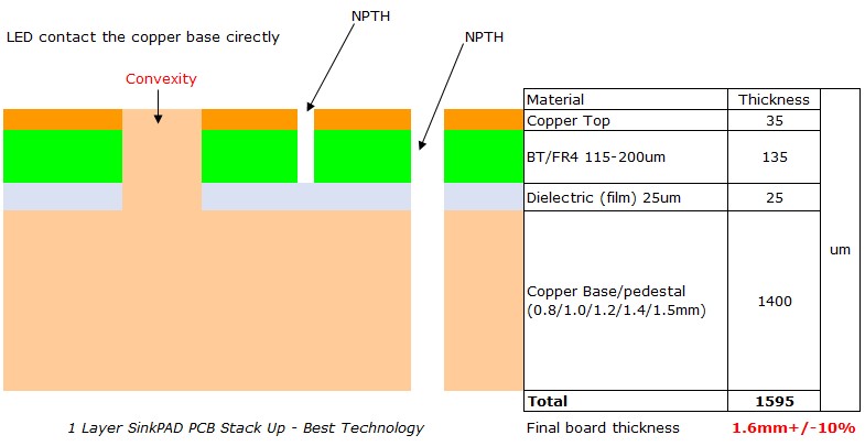
            EBest Circuit (Best Technology) – A Leading MCPCB Manufacturer in Asia

            With 18+ years of experience in the PCB industry, EBest Circuit (Best Technology) has a deep understanding of the complexities involved in MCPCB production. Our team of experts is adept at designing and manufacturing MCPCBs that deliver optimal performance. EBest Circuit (Best Technology) offers customized turn-key solutions tailored to the specific needs of our clients. Whether it’s a unique design requirement or a specific material preference, we provide flexible options to meet diverse demands.

            Contact EBest Circuit (Best Technology), get your quote right now to make your own metal core circuit boards!

            You may also like