How to choose the right copper heat sink? This guide covers selection criteria, working principles, maintenance, and application scenarios for optimal performance.
- Is the radiator too heavy to affect the portability of the product?
- Is the customization cycle delaying the project progress?
- Is it difficult to match the SMT process?
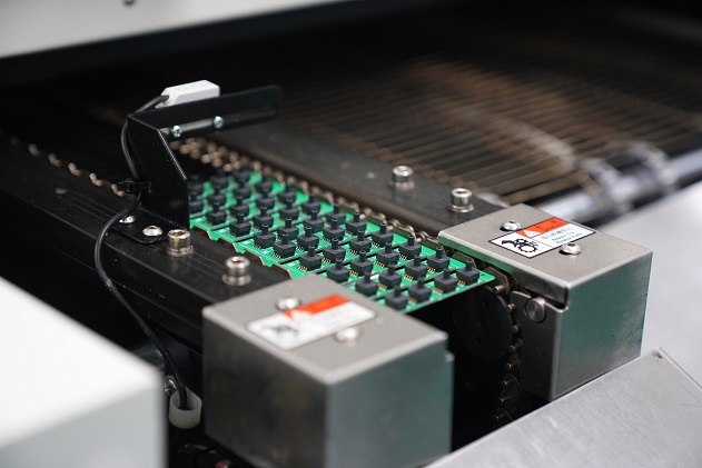
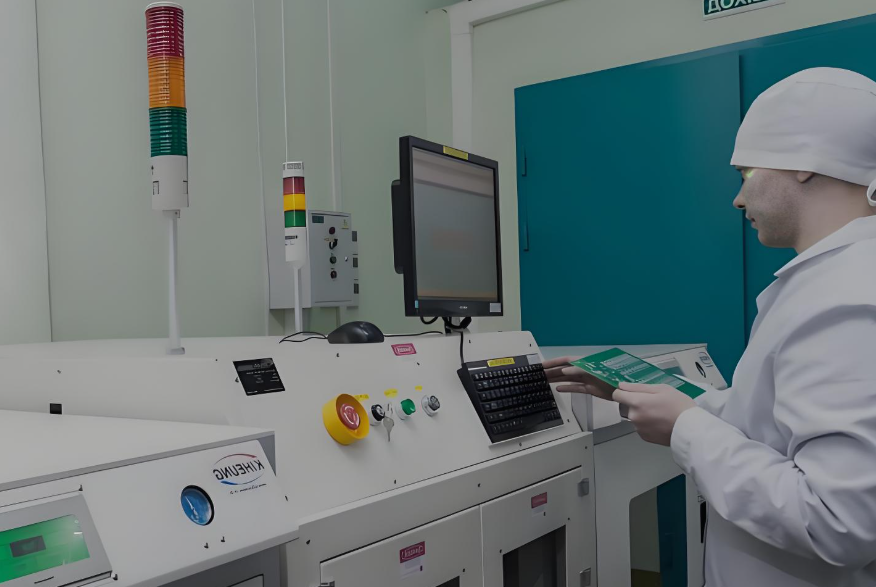
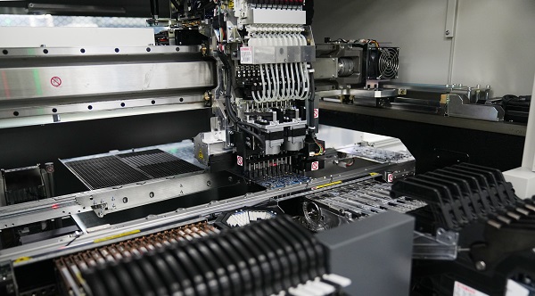
EBest Circuit (Best Technology) Can Provide You:
- Lightweight copper-aluminum composite solution: copper core + aluminum shell combination, 35% weight reduction; maintain 380W/m·K thermal conductivity.
- 72-hour fast proofing: direct selection from the existing 200+ standard parts library; support 48-hour feedback on 3D drawings.
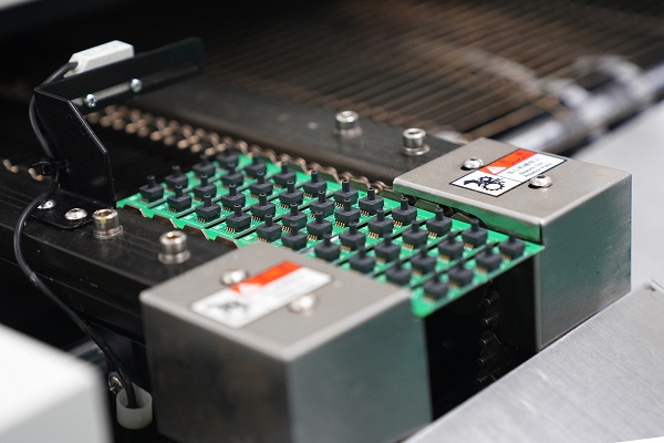
- Full process compatible design: pre-nickel plating (can be reflow soldered); provide steel mesh opening solution.
Welcome to contact us if you have any request for PCBA service: sales@bestpcbs.com.
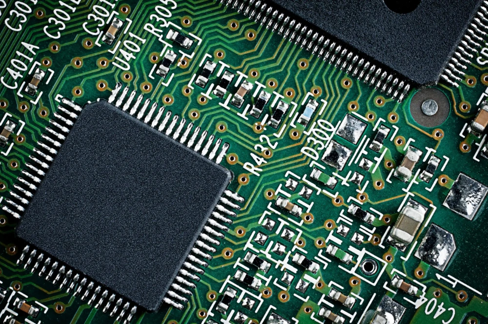
What Is A Copper Heat Sink?
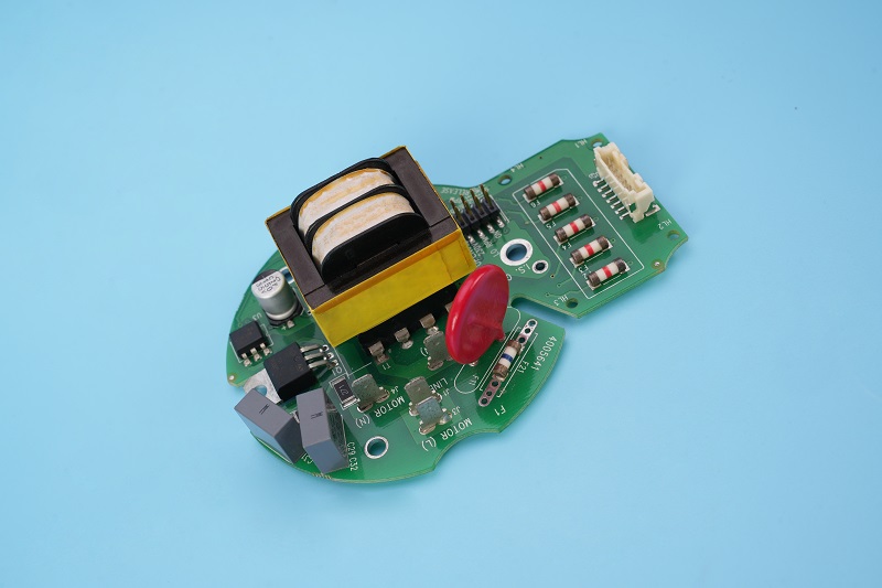
A copper heat sink is a thermal management component that utilizes copper’s high conductivity (≥350W/m·K) to absorb and disperse heat from electronic devices. Its solid metal base directly contacts heat sources like CPUs, while extended fins or pins increase surface area for efficient convection cooling. This passive design prevents overheating without moving parts, making it ideal for computers, LED systems, and power electronics where reliability and rapid heat transfer are essential.

How to Choose the Right Copper Heat Sink?
Methods about how to choose the right copper heat sinks for your project:
Thermal Performance Evaluation
- Calculate required heat dissipation capacity based on component’s max TDP (Thermal Design Power).
- Ensure copper’s thermal conductivity (≥350 W/m·K) matches your heat transfer needs.
- For high-power applications (>100W), consider vapor chamber integration.
Design Optimization
- Select fin density (4-8 fins/cm) balancing surface area and airflow resistance.
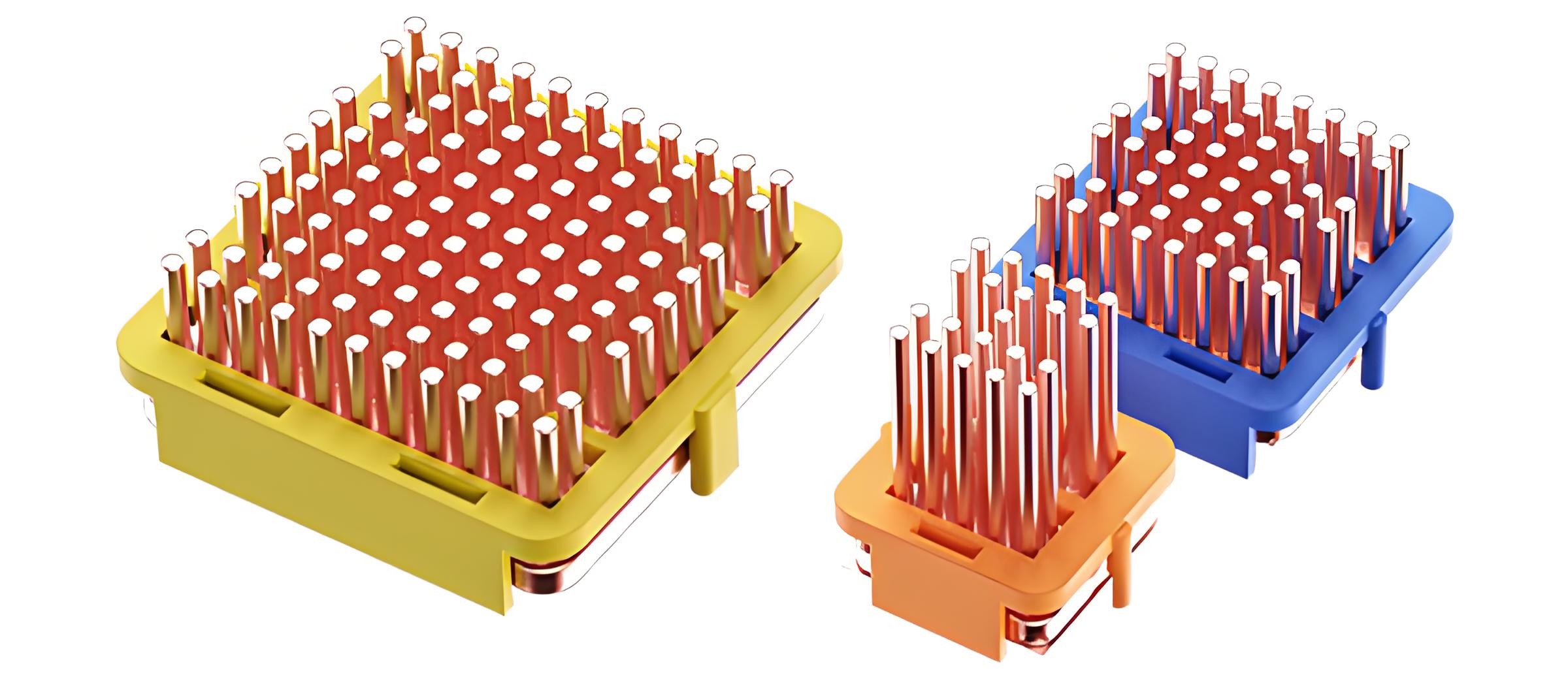
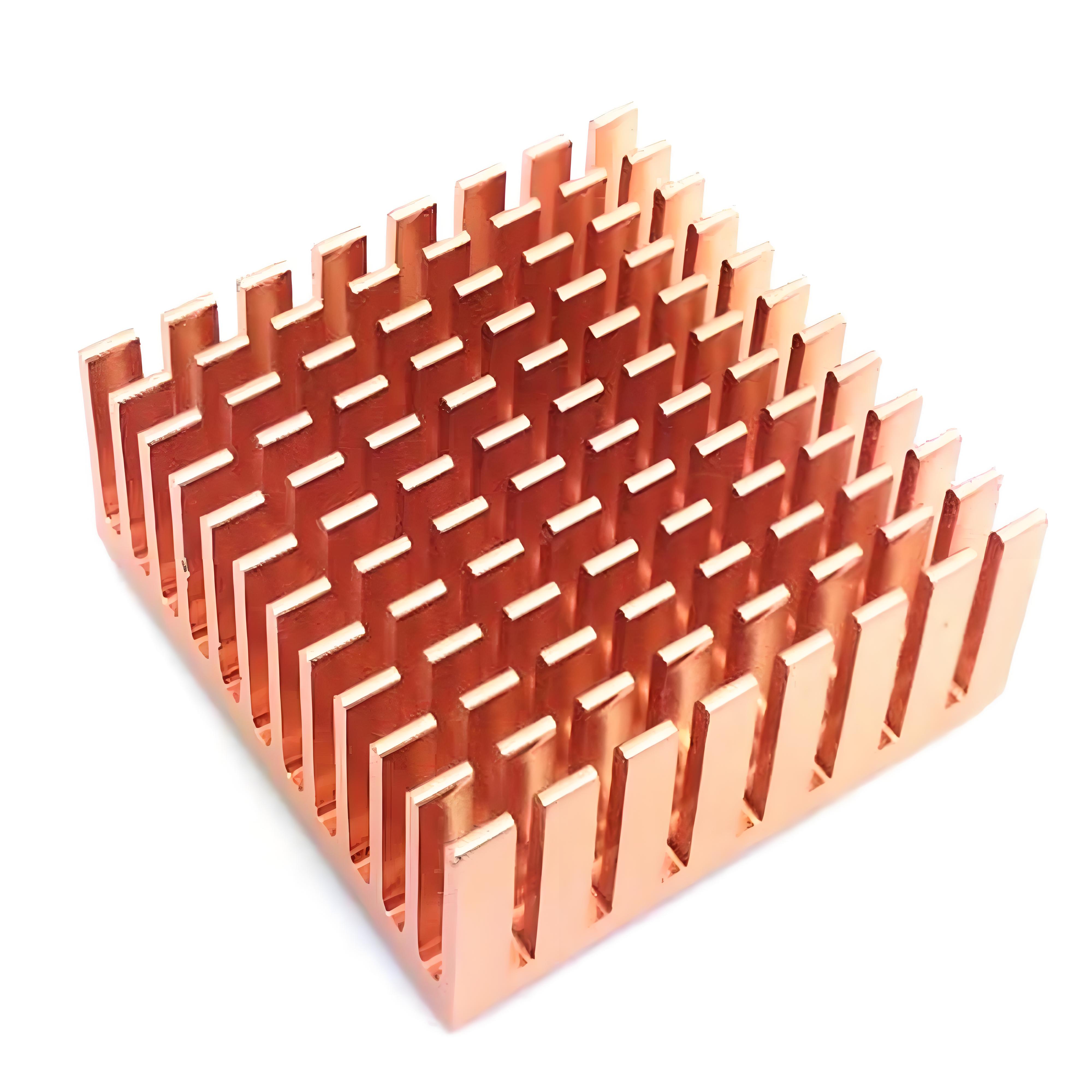
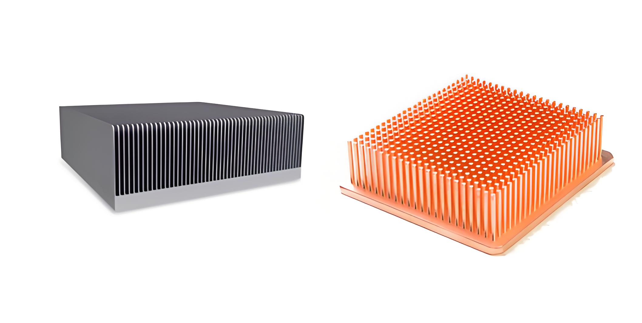
- Prefer pin-fin designs for omnidirectional airflow, straight fins for directional cooling.
- Optimal base thickness: 6-10mm for effective heat spreading.
Compatibility Checklist
- Verify mounting mechanism matches your socket type (LGA/AM).
- Measure clearance: ≥5mm from RAM slots, ≥15mm from case side panel.
- Check weight limits (<500g for vertical motherboard mounting).
Cooling Method Selection
- Passive cooling: Suitable for TDP <65W in well-ventilated cases.
- Active cooling: Required for TDP >95W or restricted airflow environments.
- Hybrid solutions: Combine copper base with heat pipes for balanced performance.
Quality Indicators
- Look for oxygen-free copper (C10100/C10200) for best thermal performance.
- Verify nickel plating thickness (≥5μm) for corrosion resistance.
- Check flatness tolerance (<0.1mm) for optimal contact with heat source.
Performance Validation
- Request thermal resistance data (℃/W) from manufacturer.
- Compare with independent test results when available.
- Ensure temperature delta (component-to-ambient) stays within safe limits.
What Are Functions of Copper Heat Sinks?
- High-Efficiency Heat Absorption: Copper’s thermal conductivity (385 W/m·K) rapidly draws heat from hot components (e.g., CPU/GPU dies), reducing localized hotspots.
- Uniform Heat Distribution: Evenly spreads thermal energy across fins/base due to copper’s isotropic conductivity, preventing thermal throttling.
- Optimized Heat Dissipation: Finned/pin designs maximize surface area (up to 30% more effective than flat designs) for faster convection cooling.
- Compatibility with High-TDP Components: Supports 150W+ TDP loads (e.g., overclocked CPUs) without phase-change materials, unlike aluminum alternatives.
- Long-Term Stability: Oxidation-resistant coatings (e.g., nickel plating) maintain >95% thermal performance over 5+ years.
- Space-Efficient Cooling: Achieves equivalent cooling performance with 20-30% smaller volume vs. aluminum, critical for compact builds.
- Hybrid Cooling Readiness: Seamlessly integrates with heat pipes/vapor chambers for extreme heat loads (e.g., data center GPUs).
- EMI Shielding Bonus: Copper’s inherent electromagnetic interference reduction protects sensitive electronics (unlike aluminum).
How Copper Heat Sinks Work?
- Thermal Conduction Initiation: Copper’s crystalline structure enables rapid electron movement, transferring heat at 401 W/m·K (25°C) from component contact surfaces within 0.5ms latency.
- Lateral Heat Spreading: Baseplate thickness (6-10mm standard) ensures 92-96% heat distribution uniformity, reducing hotspot differentials to <3°C across 100mm² areas.
- Fin-Assisted Convection: Extruded fins (12-25 fins/inch) increase effective surface area by 5-8x, achieving 18-22°C temperature drop at 2.5m/s airflow velocity.
- Thermal Interface Optimization: Micro-smooth surfaces (Ra<0.1μm) combined with thermal paste fill microscopic gaps, achieving <0.15°C/W interface resistance.
- Dynamic Load Response: Copper’s 60% faster thermal response than aluminum stabilizes component temperatures within ±2°C during 100W load fluctuations.
- Structural Heat Storage: High volumetric heat capacity (3.45 J/cm³·K) temporarily absorbs sudden thermal spikes (e.g., GPU boost clocks).
- Oxidation Mitigation: Nickel-plated surfaces maintain >90% original conductivity after 10,000 hours in 85°C/85%RH environments.
What Are Applications of Copper Heat Sink?
- Thermal Conduction Initiation: Copper’s crystalline structure enables rapid electron movement, transferring heat at 401 W/m·K (25°C) from component contact surfaces within 0.5ms latency.
- Lateral Heat Spreading: Baseplate thickness (6-10mm standard) ensures 92-96% heat distribution uniformity, reducing hotspot differentials to <3°C across 100mm² areas.
- Fin-Assisted Convection: Extruded fins (12-25 fins/inch) increase effective surface area by 5-8x, achieving 18-22°C temperature drop at 2.5m/s airflow velocity.
- Thermal Interface Optimization: Micro-smooth surfaces (Ra<0.1μm) combined with thermal paste fill microscopic gaps, achieving <0.15°C/W interface resistance.
- Dynamic Load Response: Copper’s 60% faster thermal response than aluminum stabilizes component temperatures within ±2°C during 100W load fluctuations.
- Structural Heat Storage: High volumetric heat capacity (3.45 J/cm³·K) temporarily absorbs sudden thermal spikes (e.g., GPU boost clocks).
- Oxidation Mitigation: Nickel-plated surfaces maintain >90% original conductivity after 10,000 hours in 85°C/85%RH environments.
How to Clean Copper Heat Sink?
Tools Needed: Compressed air, soft-bristle brush, lint-free cloths, 91%+ isopropyl alcohol (IPA), distilled white vinegar, baking soda, cotton swabs, plastic tweezers.
1. Disconnect & Disassemble
- Power off device; remove heat sink from component.
- Detach fans/liquid cooling tubes to access fins and baseplate.
2. Dry Dust Removal
- Blow compressed air (30+ PSI) perpendicular to fins to eject loose debris.
- Gently brush fins with soft nylon brush (>15mm bristle length) in fin direction—avoid bending fins.
3. Dissolve Oxidation (if present)
- Mix 1:1 distilled white vinegar and distilled water.
- Dip lint-free cloth, wring until damp (not dripping). Wipe oxidized areas for ≤30 seconds.
- Immediately neutralize with baking soda paste (1 tbsp soda : 3 tbsp water). Rinse under distilled water within 20 seconds.
4. Remove Thermal Paste Residue
- Apply 91%+ IPA to cotton swab. Rub old paste in circular motions until residue lifts.
- For stubborn paste, place IPA-soaked cloth on residue for 60 seconds before wiping.
- Do not scrape, copper scratches at 3+ Mohs hardness.
5. Final Rinse & Dry
- Rinse entire sink under distilled water (tap water causes mineral spots).
- Air-dry vertically for ≥10 minutes. Accelerate drying with low-pressure compressed air.
Difference: Aluminum vs Copper Heat Sink
| Property | Copper Heat Sinks | Aluminum Heat Sinks | User Impact |
| Thermal Conductivity | 385-412 W/m·K (25°C) | 205-250 W/m·K (25°C) | Copper transfers heat 55-65% faster for high-TDP components (>150W) |
| Density | 8.96 g/cm³ | 2.70 g/cm³ | Aluminum units weigh 70% less – better for portable devices |
| Material Cost | 8.50−12/kg (2025 prices) | 2.20−3.80/kg (2025 prices) | Aluminum saves 60-75% on raw material costs |
| Machining Difficulty | Harder (3.0 Mohs) | Easier (2.75 Mohs) | Aluminum allows thinner fins (0.8-1.2mm) vs copper (1.5-2.0mm minimum) |
| Oxidation Resistance | Requires nickel plating (≥5μm) | Naturally forms protective Al₂O₃ layer | Aluminum needs less maintenance in humid environments |
| Thermal Capacity | 3.45 J/cm³·K | 2.42 J/cm³·K | Copper better handles sudden heat spikes (e.g., GPU boost clocks) |
| Compatibility | May cause galvanic corrosion with aluminum | Non-reactive with most metals | Copper requires anti-corrosion measures in mixed-metal systems |
| Typical Applications | High-end CPUs/GPUs, overclocking rigs | Consumer electronics, LED lighting | Copper for performance-critical systems, aluminum for cost-sensitive builds |
Should I Buy a Copper Heat Sink for CPU?
Yes, if your CPU is high-TDP (95W+), overclocked, or requires extreme thermal performance; otherwise, no aluminum or hybrid (copper-base + aluminum-fin) coolers offer better cost-efficiency for mainstream use.
Copper’s superior thermal conductivity (~400 W/m·K) makes it ideal for demanding scenarios, but its higher cost, weight, and potential compatibility risks (e.g., motherboard strain) justify alternatives for lower-TDP CPUs. Hybrid designs balance performance and affordability, while pure aluminum suffices for low/mid-tier chips. Always pair the cooler with quality thermal interface material (TIM) and verify physical fitment (size/weight) for your build.
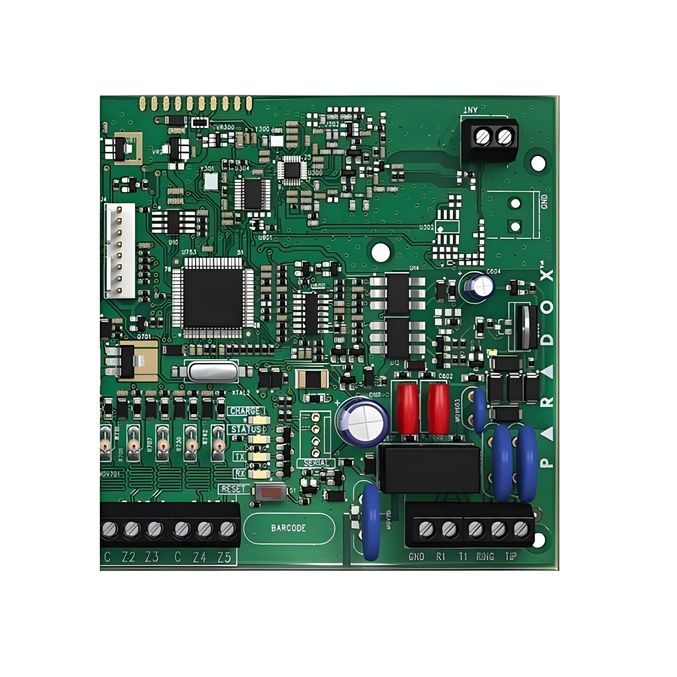
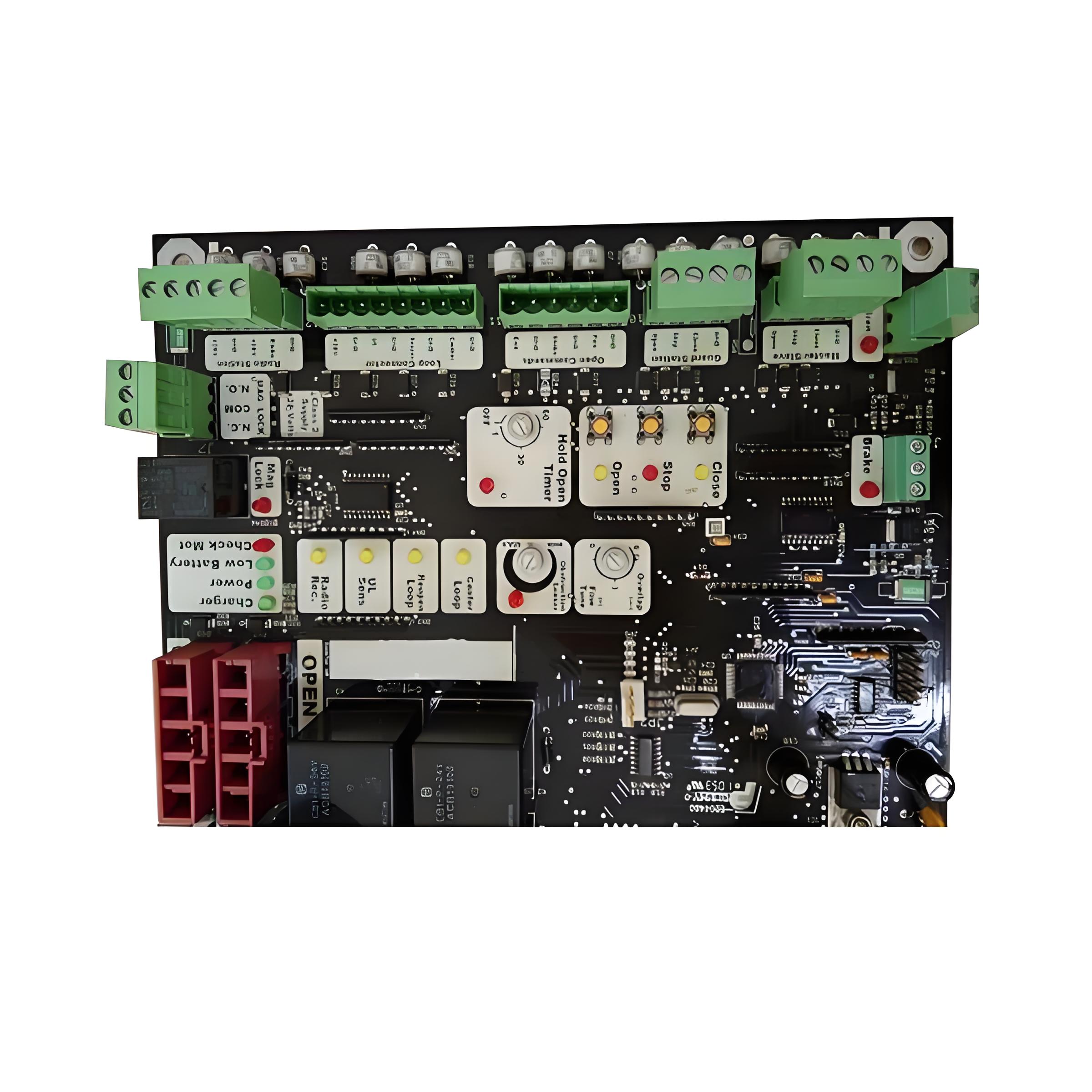
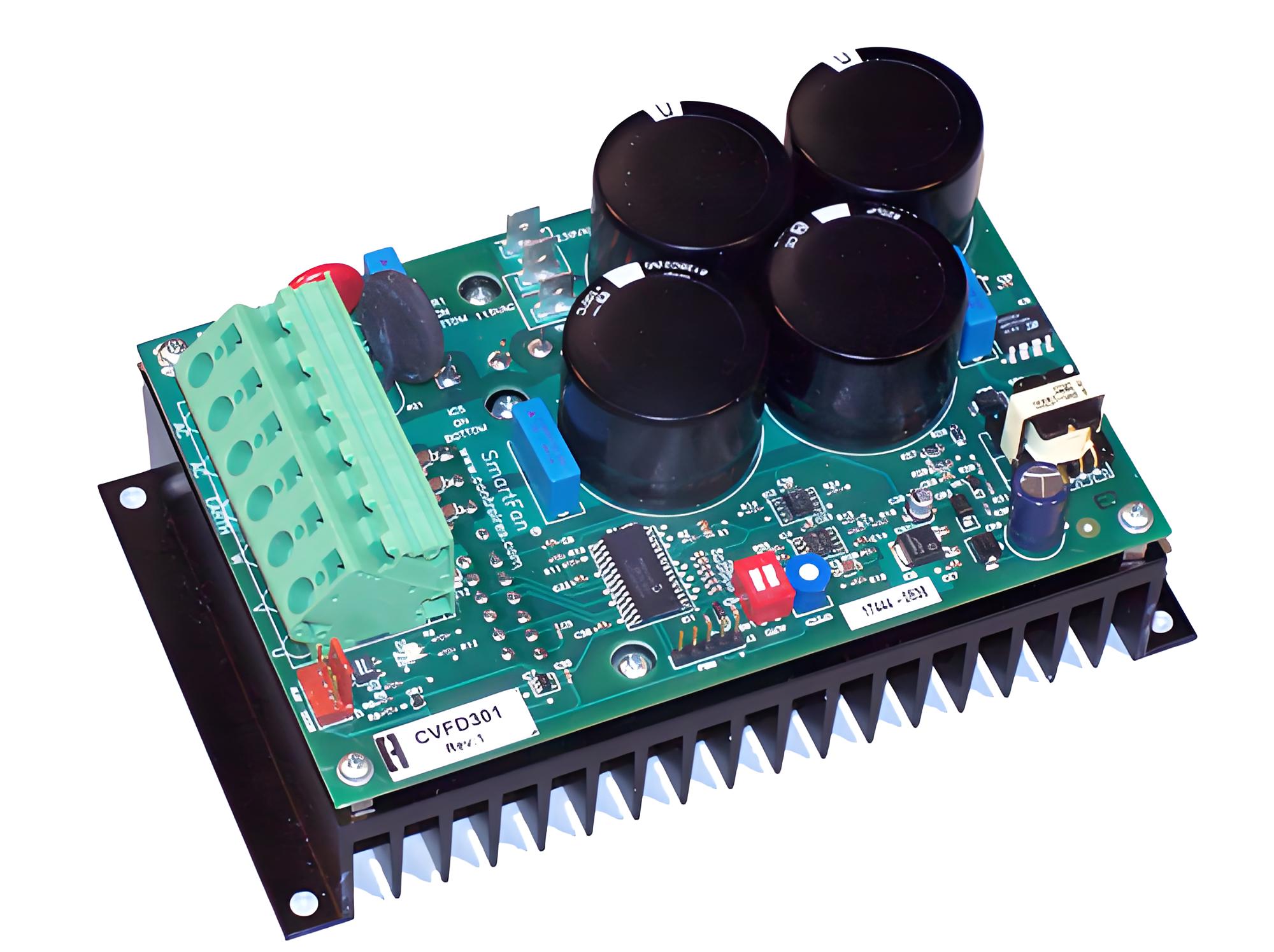
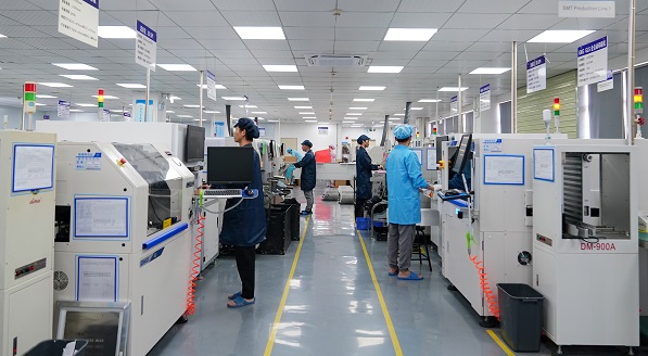
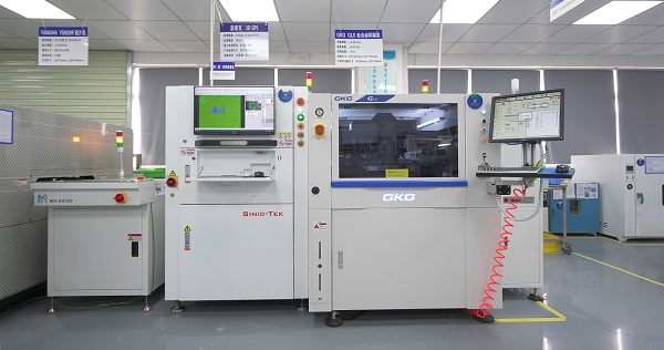
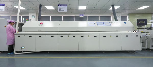
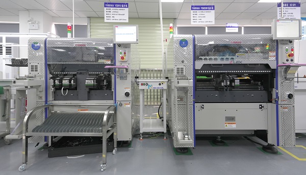
Copper Heat Sink Supplier & PCBA Service- EBest Circuit (Best Technology)
High-Efficiency Copper Heat Sinks
- Customized designs reduce hotspot temperatures by 18-25°C.
- 99.9% oxygen-free copper with optional nickel plating.
Agile Supply Chain
- 48 hours quotation turnaround with 98% on-time delivery record.
- Buffer stock for 50+ common PCB footprints.
Cost-Optimized Manufacturing
- 15% cost reduction via in-house stamping & CNC machining.
- MOQ flexibility (from 100pcs prototype batches).
End-to-End PCBA Service
- SMT-compatible designs save 2 assembly steps.
- Full traceability with IPC-A-610 Class 2/3 options.
Thermal Solution Consulting
- Free CFD simulation identifies optimal airflow paths.
- On-site thermal testing with report documentation.
Rapid Prototyping
- 5-day sample lead time with DFM feedback.
- Compatible with Altium/Mentor design files.
Global Logistics Support
- Pre-shipment thermal validation testing.
- OEM/ODM packaging with barcode tracking.
Welcome to contact EBest Circuit (Best Technology) if you need our PCBA service: sales@bestpcbs.com.