PCB manufacturing PCB manufacturing
Home > Blog

Bus Bar PCB

April 8th, 2026

EBest Circuit (Best Technology) brings nearly 20 years of PCB manufacturing experience to high-current and power distribution projects. We provide one-stop support for bus bar PCB solutions, covering layout review, engineering evaluation, prototyping, mass production, and after-sales service.

Our manufacturing system is backed by ISO9001, ISO13485, IATF16949, and UL certifications, helping customers build reliable products for demanding industries. Whether you need a custom embedded bus bar PCB, copper inlay PCB, or extruded copper PCB, our team can tailor the structure to your current, thermal, and mechanical requirements.

What is Bus Bar PCB?
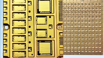
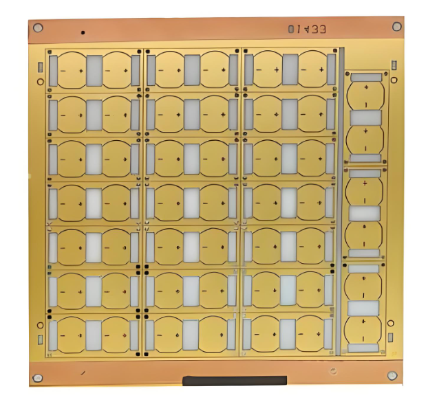
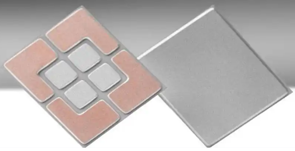
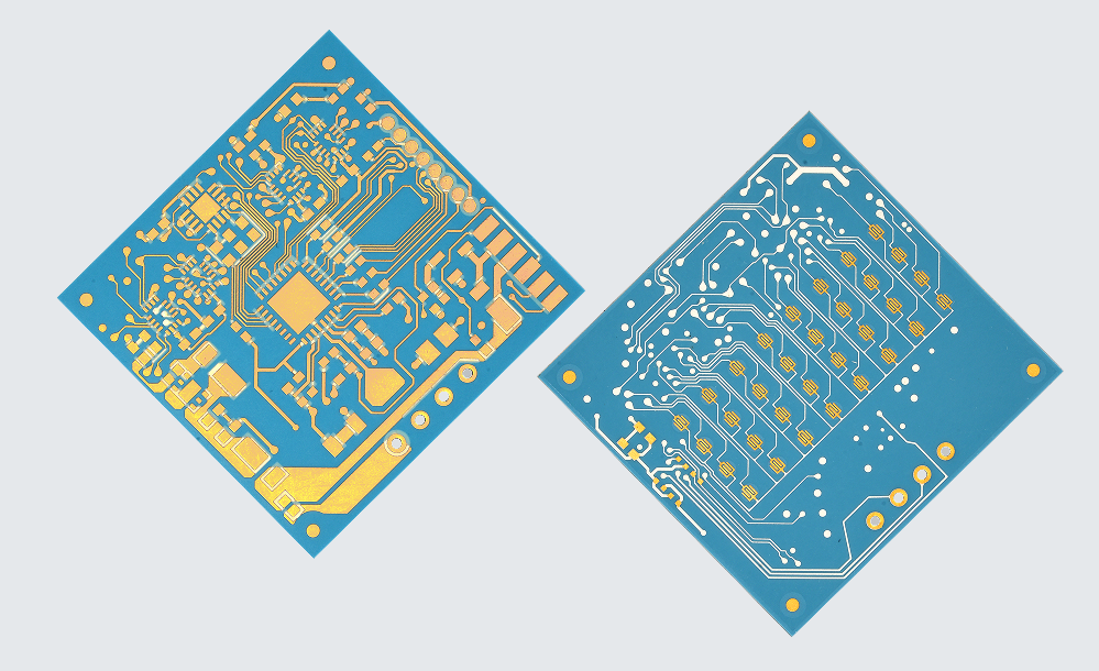
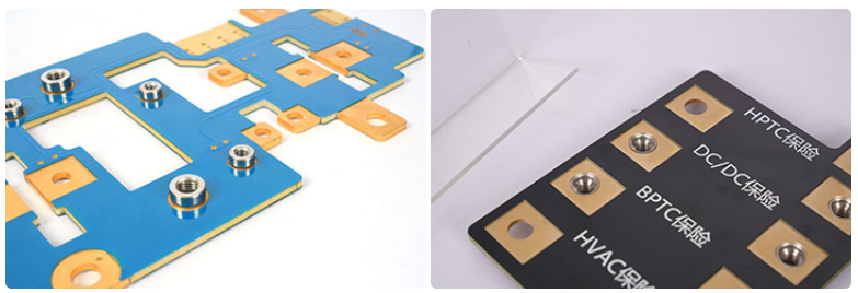
bus bar PCB, also known as an embedded bus bar, busbar PCB, extruded copper PCB, or copper inlay PCB, is a specialized type of heavy copper PCB designed specifically to distribute power efficiently across different components on a board. Unlike traditional PCBs, which use copper traces etched into layers of non-conductive substrate to form circuits, bus bar PCBs integrate thick, solid bars of conductive material—often copper or aluminum—to handle higher currents.

The bus bar PCBs can also serve as mechanical connectors within the system, designed to accommodate screws and other metal parts for direct connections with other PCBs or system components.

Bus Bar PCB

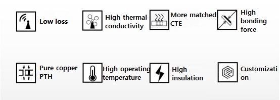
Advantages of Bus Bar PCB

  • The PCB stiffener busbars can increase the rigidity and strength of circuit boards, so they can be used in severe environments like automotives, military instruments, aerospace, etc.
  • Higher power distribution and current-carry capabilities for power supply circuits or high-power applications.
  • The low voltage drop characteristic allows all components to maintain stable power delivery, especially under high load conditions.
  • The conductive bars inĀ bus bar PCBs acts as an effective heat sink, helping to dissipate heat more efficiently than standard fiberglass PCBs, avoiding overheating problems during use.
  • The ability to handle higher currents simplifies the design and assembly process without the need for multiple layout or complex traces.
  • Bus bar PCBsĀ can be used as electrical conduit, can also be used as mechanical connector.
  • They are often custom designed to meet specific application requirements, providing solutions that are not possible with standard PCB technology.

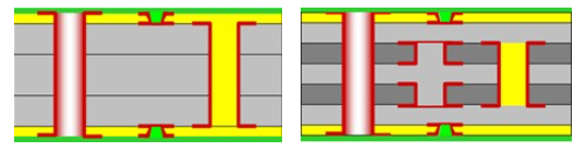
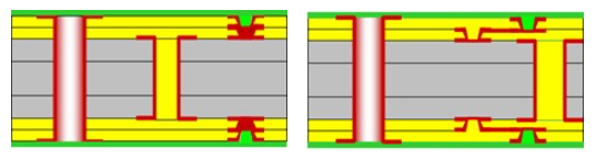
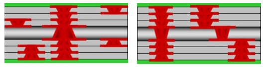
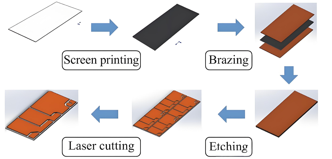
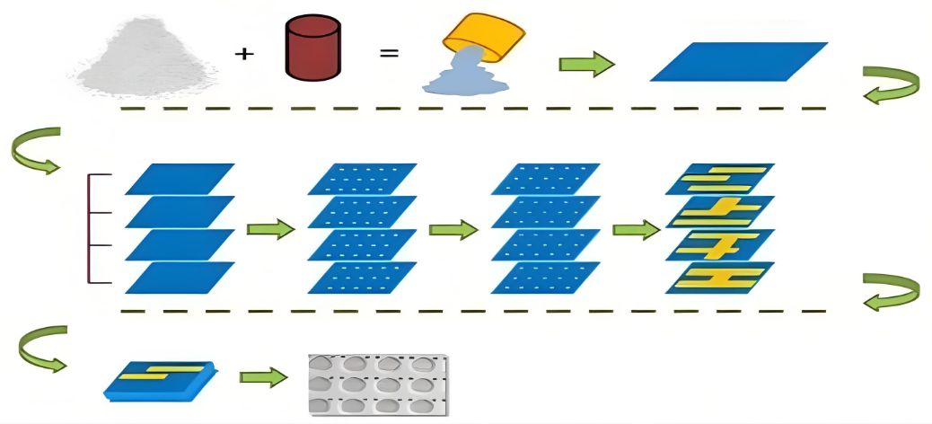
Basic Parameter of Bus Bar PCB Manufacturing

At EBest Circuit, bus bar PCB manufacturing can be customized according to current demand, installation method, and product structure. Typical capabilities include:

  • Minimum spacing between copper bars: 0.8–1.0mm
  • Copper bar thickness: 1.0–3.0mm
  • Current carrying capacity: 50–300A
  • Copper bar forming: bars can be bent based on project requirements
  • Surface finish options: ENIG, immersion silver, gold plating
  • Board thickness: 3.0–6.0mm
  • Hole wall copper thickness: ≄25um
  • Aspect ratio: 1:6 or 1:7
  • Example: for 1.0mm copper, minimum hole size can be 0.7mm
  • Layer count: typically 3–4 layers, with additional layers available after engineering review
  • Maximum dimension is 600*400mm for standardĀ bus bar PCB, 900*600mm for double sided PCB
  • The lead time of 3-4LĀ bus bar PCBĀ is around 13-15days, add 3days per layer over 4 layers.

These values may vary depending on the bus bar design, material selection, drilling limitations, and final assembly requirements.

Design Guide for Bus Bar PCB

  • Copper or aluminum is typically used for the bus bars due to their excellent conductivity and thermal properties. Copper is more conductive, while aluminum is lighter and offers better resistance to oxidation.
  • Choose substrates capable of handling high thermal loads and providing good electrical insulation. Common material we used is FR-4.
  • Determine the maximum current that each busbar needs to carry, so we can know the required cross-sectional area of the bus to minimize drag and heat buildup.
  • Use the length of the bus and the resistivity of the material to calculate the allowable voltage drop on the bus to ensure that it remains within an acceptable range.
  • Add mechanical mounting points to the bus, such as screw holes or connector slots.
  • Consider the mechanical stresses that the PCB may encounter, ensuring that the bus is flexible enough to withstand bending and strong enough to support structural loads.

Where Are Bus Bar PCBs Used?

Bus bar PCBs are used in products that require strong current handling, efficient heat control, and compact power routing. Common applications include:

  • Electric vehicles
  • Renewable energy systems
  • Industrial automation equipment
  • Power distribution units
  • Data center power systems
  • High-power spacecraft electronics
  • Consumer electronics with heavy current demand
  • Power inverters and converters
  • Aerospace and defense systems

In these fields, designers often need a solution that goes beyond standard heavy copper routing. Bus bar PCBs provide a practical way to combine power transmission, thermal performance, and mechanical integration in one board structure.

Need a Custom Bus Bar PCB?

If you are developing a high-current product and need a reliable bus bar PCB manufacturer, EBest Circuit can help. We support custom structures based on your current load, board dimensions, copper thickness, thermal requirements, and assembly needs.

Send us your drawings, Gerber files, or project requirements, and our team will review the design and provide a suitable manufacturing solution.

HDI PCB

April 8th, 2026

HDI PCB, or High Density Interconnect printed circuit board, is built for electronic products that demand more routing space, finer features, smaller vias, and higher circuit density in a limited footprint. Compared with conventional PCB structures, HDI boards support finer lines and spaces, smaller capture pads, and more interconnections per unit area, making them ideal for compact, lightweight, and high-speed devices.

At Best Technology, we provide standard HDI PCB, HDI flex PCB, 2–16 layer HDI multilayer PCB, any-layer HDI PCB, rigid-flex PCB, and high-frequency PCB solutions for customers who need reliable performance, stable manufacturing, and fast turnaround. Our uploaded source also states a monthly production capacity of 260,000 square feet (28,900 square meters), with expedited service available for urgent projects.

What Is HDI PCB?

HDI PCB is the abbreviation of High Density Interconnect PCB. It is a printed circuit board designed with high integration, high precision, and miniaturized interconnection structures. HDI technology uses advanced processes such as microvia formation, via filling, and metallized interconnection to achieve reliable signal transmission and dense circuit routing.

In practical terms, HDI PCB helps designers place more functions into a smaller board area. This makes it a preferred solution for modern electronics that require smaller product size, lighter weight, faster data transfer, and improved electrical performance. The source material describes HDI boards as having finer lines and spaces below 100 μm, smaller vias below 150 μm, and smaller capture pads below 400 μm than conventional PCB technology.

HDI PCB

Why Choose HDI PCB?

HDI PCB is widely used because it gives engineers more design freedom without sacrificing reliability.

Higher Circuit Density

HDI boards use tighter routing, smaller line width and spacing, and more advanced via structures. This allows more components and more functions to fit into the same board outline.

Better Signal Performance

Shorter signal paths and lower impedance help reduce signal delay and transmission loss. This is especially valuable in high-speed digital and high-frequency electronic applications.

Smaller and Lighter Product Design

HDI construction supports thinner, lighter, and more compact products. It is well suited to the ongoing trend toward portable and space-saving electronics.

Strong Reliability

With precise layer buildup, microvia structures, and better interlayer support, HDI boards can provide stable electrical performance and dependable mechanical structure in demanding assemblies.

Our HDI PCB Capabilities

We support a wide range of HDI PCB manufacturing solutions for both prototype and production requirements, including:

ItemCapability
Layer Count2–16 Layers (HDI), Any-Layer HDI Available
Min Line Width / Space3/3 mil (HDI)
Min Via Size~4 mil (Laser Microvia)
Via TypeBlind, Buried, Microvia, Via-in-Pad
Copper Thickness0.5 oz – 3 oz
Surface FinishENIG, ENEPIG, OSP, HASL, Immersion Silver
Board Thickness0.2 mm – 3.2 mm
BGA CapabilityDown to 0.3–0.4 mm pitch
Material OptionsFR4, High-Tg, Low Dk/Df, Polyimide
Max Panel SizeUp to 1200 mm Ɨ 360 mm
TestingAOI, X-Ray, Flying Probe, ICT

We also support fast-response manufacturing for urgent orders. According to the provided content, urgent boards can be shipped within 24 hours under suitable project conditions.

HDI PCB Types

According to layer up different, currently DHI board is divided into three basic types:

1) HDI PCB (1+N+1)

HDI PCB (1+N+1)

Features:

  • Suitable for BGA with lower I/O counts
  • Fine line, microvia and registration technologies capable of 0.4 mm ball pitch
  • Qualified material and surface treatment for Lead-free process
  • Excellent mounting stability and reliability
  • Copper filled via

Application: Cell phone, UMPC, MP3 Player, PMP, GPS, Memory Card

2) HDI PCB (2+N+2)

HDI PCB (2+N+2)

Features:

  • Suitable for BGA with smaller ball pitch and higher I/O counts
  • Increase routing density in complicated design
  • Thin board capabilities
  • Lower Dk / Df material enables better signal transmission performance
  • Copper filled via

Application: Cell phone, PDA, UMPC, Portable game console, DSC, Camcorder

3) ELIC (Every Layer Interconnection)

ELIC (Every Layer Interconnection)

Features:

  • Every layer via structure maximizes design freedom
  • Copper filled via provides better reliability
  • Superior electrical characteristics
  • Cu bump and metal paste technologies for very thin board

Application: Cell phone, UMPC, MP3, PMP, GPS, Memory card.

What is HDI Material?

1. Substrate

The substrate is the basis of HDI PCB. Commonly used organic insulating materials include thermosetting resins (such as phenolic resins and epoxy resins) and thermoplastic polyesters (such as polyimide and polytetrafluoroethylene). The choice of substrate depends on the needs of specific applications, such as rigid or flexible PCBs.

2. Copper foil

As a conductive material, the thickness of copper foil is generally between 0.3mil-3mil. The specific choice depends on the current carrying size and etching accuracy. The quality of copper foil directly affects the surface quality and electrical performance of the product.

3. PP (B-stage resin)

When making multi-layer PCBs, PP is an indispensable material as an interlayer adhesive.

4. Photosensitive materials

Including photoresists and photosensitive films, divided into wet films and dry films. These materials will undergo chemical changes under light of a specific wavelength, affecting their solubility in the developer, thereby achieving precise production of circuits.

5. Solder mask (ink)

As a solder mask, solder mask is used to prevent the adhesion of liquid solder, and its performance affects the welding quality and circuit protection of PCBs.

6. Film

Similar to the polyester film used for photography, the film is used to record image data and requires high contrast, sensitivity and resolution while ensuring fine lines and dimensional stability.

HDI PCB Manufacturing Process

The uploaded source outlines a typical HDI PCB manufacturing flow, covering the core steps from design to final inspection.

1. Design Review – define the circuit structure, layer count, and stackup

2. Material Preparation – prepare substrate, copper-clad material, covering layers, and inner layers

3. Laser Drilling – create small vias for interlayer electrical connection

4. Lamination – press the inner and outer layers into a stable structure

5. Etching – remove excess copper and keep the required conductive pattern

6. Plating – improve conductivity and oxidation resistance

7. Assembly – insert and solder components if assembly service is included

8. Testing and Inspection – verify quality and electrical performance

Typical Applications

HDI PCB is widely used in products that require compact design and high functional density. The original material lists applications such as:

  • Cell Phones
  • UMPC
  • PDA
  • GPS Devices
  • Memory Cards
  • Portable Game Consoles
  • Digital Cameras
  • Camcorders
  • Notebook Computers
  • Network Communication Equipment
  • Chip Carriers for Large-Scale IC Packaging

Why Work With EBest Circuit?

We position HDI PCB service around what engineering teams and sourcing teams actually need: broad process coverage, quick response, stable quality, and one-stop manufacturing support. The source content also highlights experience in high-end HDI, multilayer PCB, high-frequency PCB, high-speed PCB, FPC, rigid-flex PCB, SMT processing, and PCBA OEM service.

What You Can Expect

  • Wide HDI product range
  • Prototype to production support
  • Fast turnaround for urgent projects
  • One-stop PCB and PCBA service
  • Competitive pricing with manufacturing support

FAQs About HDI PCB

1. What is the difference between HDI PCB and standard PCB?

HDI PCB uses finer lines, smaller vias, and higher connection density, allowing more circuits in less space compared to standard PCB.

2. When should I use HDI PCB?

HDI is recommended when your design includes fine-pitch BGA, high-speed signals, or strict space constraints.

3. Is HDI PCB more expensive?

Yes, due to more complex processes and tighter tolerances. However, it can reduce overall system size and improve performance.

4. What is the minimum via size in HDI PCB?

Typically around 4 mil (laser drilled microvia), depending on manufacturer capability.

5. Can HDI PCB improve signal integrity?

Yes. Shorter routing paths and better layer control can improve signal performance in high-speed designs.

6. How long does HDI PCB manufacturing take?

Prototype lead time can be as fast as 24 hours, while standard production depends on complexity and volume.

Get a Quote for Your HDI PCB Project

If your project requires microvias, fine-pitch BGA routing, higher wiring density, or compact multilayer construction, HDI PCB may be the right solution. A well-designed HDI board can help reduce product size, improve routing efficiency, and support stronger electrical performance in advanced electronics.

Send us your Gerber files, stackup requirements, and project specifications. Our team can review your design and recommend a suitable HDI PCB manufacturing solution.

Metallized Ceramic Substrate

April 3rd, 2026

Metallized ceramic substrate is the critical foundation for high-temperature, high-power, and mission-critical electronic designs—indispensable for medical devices, aerospace systems, and industrial equipment. Selecting the right metallized ceramic substrate directly impacts thermal performance, signal integrity, and long-term reliability. This expert guide covers everything you need to know about metallized ceramic substrate, from core principles to real-world solutions and trusted manufacturing.

Metallized Ceramic Substrate

Metallized Ceramic Substrate

What Is Metallized Ceramic Substrate & How Does It Work?

A metallized ceramic substrate consists of a ceramic base (Alā‚‚Oā‚ƒ, AlN, Siā‚ƒNā‚„) with precision-bonded metal layers, combining ceramic’s excellent thermal conductivity and electrical insulation with metal’s electrical conductivity. It efficiently dissipates heat from high-power components, solving the thermal bottleneck of standard PCBs.

Core Structure

Ceramic insulating layer: Provides thermal dissipation and electrical isolation

Metal conductive layer: Forms circuit traces and component mounting pads

Strong metal-ceramic bond: Prevents delamination under thermal and mechanical stress

Why Use Metallized Ceramic Substrate for High-Power Electronics?

Metallized ceramic substrate delivers unmatched advantages over FR-4 and thick-film substrates in extreme operating conditions. It is the only choice for designs requiring stable performance under high heat and stress.

Key Advantages

Ultra-high thermal conductivity (up to 200 W/mĀ·K for AlN, compared to 0.35 W/mĀ·K for FR-4)

Excellent electrical insulation and high voltage breakdown resistance

Stable operation from -55°C to 200°C+

Low thermal expansion that matches silicon chips, reducing thermal fatigue

High mechanical strength and resistance to vibration and shock

Metallized Ceramic Substrate vs Thick Film vs Thin Film: Which Is Better?

Parameter | Metallized Ceramic Substrate | Thick Film Substrate | Thin Film Substrate

Thermal Conductivity | High (170–200 W/mĀ·K for AlN) | Medium (10–30 W/mĀ·K) | Low (5–15 W/mĀ·K)

Line Precision | High (50–100μm) | Medium (100–200μm) | Ultra-High (10–50μm)

Power Handling | High (kW-level) | Medium (100W-level) | Low (10W-level)

Bond Strength | Excellent | Good | Fair

Best Application | High-power, aerospace, medical | Consumer electronics, sensors | RF, microwave, precision circuits

What Materials Are Used for Metallized Ceramic Substrate?

Three primary ceramic materials are used for metallized ceramic substrates, each with unique thermal and mechanical properties tailored to specific applications.

Alumina (Alā‚‚Oā‚ƒ)

Cost-effective, high in mechanical strength, and widely adopted

Thermal conductivity: 25–35 W/mĀ·K

Ideal for general industrial, automotive, and mid-power designs

Aluminum Nitride (AlN)

Ultra-high thermal conductivity and a near-perfect thermal expansion match with silicon

Thermal conductivity: 170–200 W/mĀ·K

Best for high-power semiconductors, aerospace, and laser systems

Silicon Nitride (Siā‚ƒNā‚„)

Exceptional resistance to thermal shock and fracture

Thermal conductivity: 60–90 W/mĀ·K

Perfect for high-vibration aerospace and heavy industrial equipment

What Specifications Matter Most for Metallized Ceramic Substrate?

These critical specifications determine whether a metallized ceramic substrate will meet your design’s performance and reliability requirements.

Must-Verify Specifications

Thermal conductivity (W/mĀ·K): Matches your heat dissipation needs

Metal layer thickness and adhesion strength: Prevents delamination

Dimensional tolerance: ±0.02mm for high-precision designs

Insulation resistance and voltage breakdown rating

Plating finish (Ni/Au, ENIG): Ensures reliable soldering

Thermal expansion coefficient: Matches the attached semiconductor chips

How Is Metallized Ceramic Substrate Manufactured?

Strict process control ensures consistent quality and performance in metallized ceramic substrate production.

Step-by-Step Manufacturing Flow

Ceramic blank preparation: Precision cutting, polishing, and deep cleaning

Surface activation: Enhances metal-ceramic bonding strength

Metallization: Sputtering, screen printing, or direct metal bonding

High-temperature sintering: Forms permanent, robust metal-ceramic bonds

Photolithography and etching: Defines precise circuit patterns

Plating: Ni/Au, Ni/Pd/Au for corrosion resistance and solderability

Final inspection: 100% testing of thermal resistance, adhesion, and dimensional accuracy

Where Is Metallized Ceramic Substrate Used in Medical, Aerospace & Industry?

Metallized ceramic substrate enables mission-critical performance across high-reliability industries.

Medical Application

MRI gradient coil power modules: AlN metallized ceramic substrate dissipates 500W+ of heat with zero signal interference, ensuring clear diagnostic imaging.

Aerospace Application

Satellite DC-DC converters: Withstands extreme temperature cycles (-40°C to 150°C) and cosmic radiation, delivering 10+ years of orbital reliability.

Industrial Application

IGBT inverter substrates: Siā‚ƒNā‚„ metallized ceramic substrate resists thermal shock from thousands of on/off cycles, eliminating factory downtime.

What Are Common Failures of Metallized Ceramic Substrate & Solutions?

Top Failures & Proven Fixes

Metal-ceramic delamination: Optimize surface activation and sintering parameters; use complimentary DFM analysis to avoid design-induced stress.

Insufficient thermal dissipation: Upgrade to AlN or Siā‚ƒNā‚„ material; optimize trace layout for maximum heat spreading.

Poor solderability: Apply uniform Ni/Au plating; control surface contamination during production.

Dimensional warpage: Use precision-ground ceramic blanks; balance metallization layer thickness across the substrate.

Why Choose EBestpcb as Your Metallized Ceramic Substrate Manufacturer?

For reliable, high-performance metallized ceramic substrate, EBestpcb is your top partner.

Fast lead times for prototypes and mass production

100% quality inspection with a zero-defect guarantee

Full industry certifications for medical, aerospace, and industrial compliance

Complimentary DFM analysis to optimize your design

Flexible MOQ for prototype sampling and dedicated technical support

What Services Do We Offer for Metallized Ceramic Substrate?

We provide end-to-end solutions for metallized ceramic substrate from design to finished parts.

Custom metallized ceramic substrate design and complimentary DFM review

Material selection support (Alā‚‚Oā‚ƒ, AlN, Siā‚ƒNā‚„)

Precision metallization (sputtering, screen printing, direct bonding)

Plating services (ENIG, Ni/Au, Ni/Pd/Au)

Prototyping and mass production capabilities

Full reliability testing and quality validation

What Certifications Do We Hold for Metallized Ceramic Substrate Production?

Our certifications ensure global compliance and quality for metallized ceramic substrate.

ISO 9001: Quality management system certification

ISO 13485: Medical device manufacturing compliance

IATF 16949: Automotive quality standard

UL and RoHS certified for safety and environmental requirements

Aerospace material and process validation credentials

Our Metallized Ceramic Substrate Production Capabilities

Capability | Specification

Ceramic Materials | Alā‚‚Oā‚ƒ (96%/99%), AlN, Siā‚ƒNā‚„

Max Substrate Size | 200mm Ɨ 300mm

Thickness Range | 0.25mm – 5.0mm

Min Line Width/Space | 50μm / 50μm

Metallization Layers | Cu, Ni/Au, Ag/Pd

Plating Options | ENIG, Ni/Au, Ni/Pd/Au

Dimensional Tolerance | ±0.02mm

Thermal Conductivity | Up to 200 W/mĀ·K (AlN)

Solve Your Toughest Metallized Ceramic Substrate Challenges—Partner With EBestpcb

Engineers and teams consistently face pain points with metallized ceramic substrate: thermal bottlenecks, delamination risks, inconsistent quality, long lead times, and lack of design support. We resolve these issues with optimized material selection, strict process control, complimentary DFM analysis, fast turnaround, and full compliance certifications. For mission-critical medical, aerospace, and industrial designs, trust EBestpcb for your metallized ceramic substrate needs—we deliver performance you can count on.

FAQ: Frequently Asked Questions About Metallized Ceramic Substrate

What is the best material for high-power metallized ceramic substrate?

Aluminum Nitride (AlN) is ideal, offering ultra-high thermal conductivity and thermal expansion that matches silicon chips.

How to prevent metallized ceramic substrate delamination?

Ensure proper surface activation, controlled sintering, balanced metal thickness, and complimentary DFM analysis before production.

What industries use metallized ceramic substrate most?

Medical devices, aerospace systems, industrial power electronics, automotive inverters, and laser equipment.

What is the difference between metallized ceramic substrate and thick film substrate?

Metallized ceramic substrate offers higher thermal conductivity and power handling, while thick film is cost-effective for low-power consumer electronics.

Can you customize metallized ceramic substrate for specific applications?

Yes—we provide custom materials, sizes, thicknesses, metallization, and plating for medical, aerospace, and industrial use cases.

What certifications do you hold for metallized ceramic substrate production?

We hold ISO 9001, ISO 13485, IATF 16949, UL, and RoHS certifications for full industry compliance.

How long is the lead time for metallized ceramic substrate prototypes?

Prototype lead times start at 7–10 days, with mass production timelines optimized for your volume requirements.

DPC Ceramic PCB

April 1st, 2026

DPC (Direct Plated Copper) technology denotes a special process in which the copper foil and the Al2O3 or AlN (one or both sides) are directly plated under appropriate high temperature.

The super-thin DPCĀ substrateĀ has excellent electrical isolation, high thermal conductivity, fine solderability and high bonding strength. It can be etched like normalĀ FR4 PCB, but has a high current loading capability. ThereforeĀ DPC ceramic PCBĀ has become the base materials of construction and interconnection technology of high power semiconductor electronic circuits and also have been the basis for the “Chip On Board” (COB) technology which represent the packaging trend in the future.

Why Choose DPC Ceramic PCB?

DPC ceramic PCB is widely used in high-performance electronic packaging because it provides several practical advantages:

  • Excellent electrical insulation
  • High thermal conductivity
  • Fine line and fine spacing capability
  • Strong copper bonding strength
  • Good solderability for advanced packaging
  • High current carrying capacity
  • Suitable for miniaturized and high-density circuit designs

Another important benefit is that DPC ceramic PCB can be processed in a way similar to standard PCB etching, which gives engineers more design flexibility while maintaining the thermal and mechanical strengths of ceramic materials.

DPC Ceramic PCB

DPC Ceramic PCB

Typical Applications of DPC Ceramic PCB

Because of its structure and performance, DPC ceramic PCB is often used in:

  • High power semiconductor modules
  • LED packaging
  • RF and microwave devices
  • Automotive electronics
  • Power control systems
  • Laser devices
  • Medical electronics
  • Chip on Board (COB) packaging

DPC technology has become an important foundation for modern COB packaging and advanced electronic interconnection, especially in products where heat management and circuit precision are both critical.

Available DPC Ceramic PCB Samples

Below are some of our DPC ceramic PCB product examples for reference, you can visit the portal as below to see more product photos:

  • BCD18309 – 2 Layers, 1.5mm Ceramic PCB
  • BCD18372 – 2 Layers, 0.5mm AlN Ceramic PCB
  • BCD19449-B – 2 Layers, 1.0mm, 2oz Ceramic PCB
  • BCD20092– 2 Layers, 0.635mm Ceramic PCB
  • BCD20093 – 2 Layers, 0.635mm Ceramic PCB
  • BCD20108 – 2 Layers, 1.0mm AlN Ceramic PCB
  • BCD20109 – 2 Layers, 1.0mm Al2O3 Ceramic PCB
  • BCD20140 – 2 Layers, 1.0mm AlN Ceramic PCB
  • BCD20162 – 2 Layers, 0.635mm AlN Ceramic PCB
  • BCD20271 – 2 Layers, 0.635mm, 4oz AlN Ceramic PCB
  • BCS20051 – 1 Layer, 0.635mm, 1oz Al2O3 Ceramic PCB
  • BCS20091 – 1 Layer, 1.0mm, 1oz Al2O3 Ceramic PCB
  • BCS20228 – 1 Layer, 0.635mm, 2oz Al2O3 Ceramic PCB
  • BCS20297 – 1 Layer, 0.5mm, 5–7μm Al2O3 Ceramic PCB

Please contact us today for more information about Ceramic circuit board (Ceramic PCB).

Learn More About Our Ceramic PCB Solutions

We offer a wide range of DPC ceramic circuit boards for customers who need reliable thermal management, precise copper patterns, and stable performance in demanding environments. You are welcome to review our product portal for more sample photos and specifications.

Contact us today to learn more about our ceramic PCB manufacturing capabilities and get support for your project.

Thin Film Ceramic PCB

April 1st, 2026

Thin film ceramic PCB is a high-precision ceramic circuit solution used in applications that require fine conductor patterns, stable electrical performance, and reliable high-frequency transmission. This article explains what thin film ceramic PCB is, how it is made, what advantages it offers, and where it is commonly used.

For engineers, one of the biggest challenges in advanced circuit design is balancing miniaturization, accuracy, and signal stability. Standard PCB materials may not always perform well in microwave, RF, or precision analog environments. That is why thin film ceramic PCB has become a preferred option in sectors where dimensional control, low loss, and long-term stability matter.

What Is Thin Film Ceramic PCB?

A thin film ceramic PCB is a ceramic-based circuit board made with an ultra-thin conductive layer deposited directly onto the ceramic substrate. In most cases, the conductor thickness is less than 10 μm, which is thinner than that of a thick film ceramic PCB.

This thin conductive layer is formed by advanced deposition technologies such as:

  • Physical vapor deposition (PVD)
  • Sputtering
  • Evaporation
  • Electroplating
  • Anodic oxidation in selected applications

Because the circuit pattern can be formed with very high precision, thin film ceramic PCB is widely used in compact, high-performance electronic assemblies.

What Is Thin Film Ceramic PCB?

Thin Film Ceramic PCB

How Is Thin Film Ceramic PCB Different from Thick Film Ceramic PCB?

The biggest difference lies in the conductor thickness and fabrication method.

Thin film ceramic PCB uses deposited metal layers with very fine thickness control, while thick film ceramic PCB usually uses printed conductive paste followed by high-temperature firing. Here is a quick comparison between thin film and thick film ceramic PCB:

ItemThin Film Ceramic PCBThick Film Ceramic PCB
Conductor ThicknessUsually below 10 μmUsually above 10 μm
Fabrication MethodDeposition-basedScreen printing and firing
Line PrecisionVery highModerate
Circuit DensityHigherLower
Electrical AccuracyExcellentGood
CostHigherMore economical
Best UseRF, microwave, precision analogPower circuits, standard hybrid circuits

In short, thin film ceramic PCB is often selected when the design requires tighter tolerances and better RF behavior.

What Are the Main Characteristics of Thin Film Ceramic PCB?

Compared to thick-film ceramic PCB, the major characteristics of thin-film circuits is the smaller size. However, the manufacturing equipment used is more expensive and the cost of production is higher.

Thin-film Ceramic PCB is suitable for a variety of circuits, especially for analog circuit which need high accuracy, great stability, and excellent performance. Compared with other circuits board, it is more suitable for microwave circuits.

What Types of Thin Film Ceramic Circuits Are There?

Thin film ceramic circuits are often divided into two categories based on passive element behavior.

  • Lumped Parameter Circuits

These circuits have passive elements concentrated in specific component regions. They are commonly used from low-frequency applications up to the microwave range.

  • Distributed Parameter Circuits

In these designs, electrical parameters are distributed along the circuit geometry itself. This structure is mainly used in the microwave frequency band, where line dimensions directly affect performance.

This classification is especially relevant in RF design, where layout and material selection are closely connected.

How Is Thin Film Ceramic PCB Manufactured?

Several manufacturing methods can be used to form thin conductive layers on ceramic substrates. The most common process family is physical vapor deposition, while electroplating and anodic oxidation may also be used in selected steps.

PVD is one of the most common methods for making thin film ceramic PCB. It forms metal layers on the ceramic surface inside a vacuum chamber. The two most widely used PVD methods are:

1. Evaporation

In the evaporation process, the source material is heated until it becomes vapor, then it condenses onto the ceramic substrate as a thin and uniform film.

2. Sputtering

In sputtering, particles are ejected from a target material and deposited onto the ceramic surface. This process offers good adhesion, excellent film uniformity, and strong thickness control.

These vacuum-based methods are widely used to create:

  • Fine conductive traces
  • Resistor films
  • Insulating layers
  • Protective films
  • Passive circuit networks

What Is the Role of Electroplating in Thin Film Ceramic PCB?

Electroplating is often used as a supplementary process. In microwave hybrid integrated circuits, it can increase the thickness of selected thin film conductors, such as microstrip lines.

This helps improve:

  • Current-carrying capability
  • Conductor performance
  • Power efficiency
  • Signal transmission in certain RF structures

Electroplating is not always the main film-forming step, but it plays an important role in performance tuning.

What Is the Role of Anodic Oxidation?

Anodic oxidation is less commonly used than PVD, but it still has value in special thin film applications.

It can be used to:

  • Form dielectric films
  • Improve insulation in specific areas
  • Adjust the resistance value of some thin film resistors

For highly customized circuit structures, anodic oxidation can support better control of electrical properties.

Where Is Thin Film Ceramic PCB Used?

Thin film ceramic PCB is used in products where accuracy, stability, and high-frequency behavior are critical.

Typical applications include:

  • RF modules
  • Microwave circuits
  • Hybrid integrated circuits
  • Precision analog circuits
  • Sensors
  • Aerospace electronics
  • Medical electronics
  • Telecom equipment
  • Defense and instrumentation systems

These applications often require materials and circuit structures that can maintain performance under temperature change, frequency stress, and long operating cycles.

Why Is Thin Film Ceramic PCB Suitable for RF and Microwave Applications?

Thin film ceramic PCB is especially suitable for RF and microwave designs because it combines:

  • Fine conductor geometry
  • Stable substrate performance
  • Low dimensional variation
  • Good high-frequency consistency
  • Strong thermal stability

In microwave circuits, even small variations in line width or conductor thickness can affect impedance and signal loss. Thin film technology helps reduce that variation and supports more predictable performance.

FAQ

1. What is the conductor thickness of thin film ceramic PCB?

In most cases, the conductor thickness of a thin film ceramic PCB is less than 10 μm. That is one of the main distinctions between thin film and thick film ceramic technologies.

2. Is thin film ceramic PCB better than thick film ceramic PCB?

It depends on the application. Thin film ceramic PCB is better for high precision, RF, microwave, and compact circuit designs. Thick film ceramic PCB is often more suitable for cost-sensitive or less demanding designs.

3. Can thin film ceramic PCB be used in analog circuits?

Yes. Thin film ceramic PCB is widely used in precision analog circuits because of its stable electrical performance and fine pattern accuracy.

4. Why is thin film ceramic PCB more expensive?

The cost is higher because the process requires vacuum equipment, advanced deposition technology, and tighter manufacturing control.

5. Is thin film ceramic PCB suitable for microwave circuits?

Yes. It is one of the preferred solutions for microwave circuits because it supports fine features, stable conductor behavior, and strong high-frequency performance.

Why Choose EBest Circuit for Thin Film Ceramic PCB?

EBest Circuit has extensive experience in advanced ceramic PCB manufacturing and custom circuit solutions for demanding electronic applications. We understand that thin film ceramic PCB projects often require more than basic fabrication. They need careful material selection, precise process control, and strong engineering support from design to production.

What we can offer includes:

  • Professional ceramic PCB manufacturing experience

We support a wide range of ceramic circuit requirements, including high-precision and high-reliability applications.

  • Engineering-driven support

Our team works closely with customers on material choice, stack-up suggestions, manufacturability review, and process optimization.

  • Support for complex applications

We understand the needs of RF, microwave, hybrid, medical, and industrial customers who require stable and repeatable circuit performance.

  • One-stop service

From PCB fabrication to assembly support, we help simplify the supply chain and reduce project coordination pressure.

  • Quality-focused manufacturing

We emphasize process consistency, inspection control, and reliable delivery to support both prototype and production needs.

If you are looking for a dependable thin film ceramic PCB manufacturer, EBest Circuit is ready to support your project with practical engineering advice and responsive service.
Contact us at sales@bestpcbs.com for technical discussion and quotation support.

AMB Ceramic PCB

April 1st, 2026

AMB Ceramic PCB is a high-performance ceramic substrate designed for power electronics that demand strong copper-to-ceramic bonding, efficient heat dissipation, and long-term reliability. At Best Technology, we provide custom AMB ceramic PCB solutions using Al2O3, AlN, and Si3N4 ceramic materials for customers in automotive, industrial, energy, rail transit, and high-power semiconductor industries.

If your project requires a substrate that can handle high current, thermal cycling, and harsh operating conditions, AMB PCB is a dependable choice.

Why Choose Best Technology for AMB Ceramic PCB?

At Best Technology (EBest Circuit), we provide advanced ceramic PCB solutions tailored for high-performance applications.

Our Strengths

  • 20+ years of PCB and PCBA experience
  • Support for Al2O3, AlN, and Si3N4 substrates
  • Copper thickness up to 800 µm
  • Strong expertise in power modules and thermal design
  • Full turnkey service from PCB to assembly
  • Certified with ISO 9001, ISO 13485, and IATF 16949

We work closely with engineers to optimize designs for manufacturability, reliability, and cost efficiency.

AMB Ceramic PCB

What Is AMB Ceramic PCB?

AMB stands for Active Metal Brazing. It is a ceramic substrate technology that bonds copper foil to ceramic by using active brazing materials containing metal elements such as titanium, silver, zirconium, or copper.

Unlike standard bonding methods, AMB creates a strong chemical bond between metal and ceramic at high temperature. This gives the finished substrate:

  • Higher bonding strength
  • Better resistance to thermal stress
  • Excellent heat transfer performance
  • Higher reliability in demanding environments

AMB ceramic PCB is widely used in power modules, IGBT modules, SiC packaging, EV systems, traction inverters, and renewable energy equipment.

Why Choose AMB Ceramic PCB?

For many power electronics projects, the substrate must do more than just carry traces. It must also help control heat, maintain insulation, and survive repeated thermal cycling. AMB ceramic PCB is chosen because it offers:

  • Stronger Bonding Performance

The active metal brazing process creates a reliable bond between copper and ceramic, making the substrate more suitable for high-power module packaging.

  • Better Reliability Under Thermal Stress

AMB substrates are designed for applications with frequent temperature changes and high operating loads. In advanced module structures, they can support very high thermal shock resistance.

  • Excellent Heat Dissipation

With the right ceramic material, AMB PCB can provide strong thermal performance for power semiconductors, converters, and high-current designs.

  • Good Match for Advanced Power Devices

AMB substrates are widely used with SiC chips, silver sintering processes, and thick copper designs, where both heat and reliability matter.

AMB Ceramic PCB vs DBC Ceramic PCB

Both AMB and DBC are used in ceramic substrate manufacturing, but they are not the same.

ItemDBC Ceramic PCBAMB Ceramic PCB
Bonding methodDirect bonding of copper to ceramicActive metal brazing
Process structureSimplerMore complex
Bonding strengthGoodHigher in many demanding applications
Thermal cycling reliabilityGoodExcellent
Suitable for harsh environmentsYesBetter suited for severe conditions
Typical high-reliability useStandard power modulesEV, traction, SiC, high-reliability power modules

In short, DBC is a strong option for many standard power applications, while AMB is often preferred when stronger bonding and better long-term reliability are required.

Ceramic Materials Available for AMB PCB

We provide AMB ceramic substrates based on different ceramic materials to match different power levels, cost targets, and reliability requirements.

1. Alumina AMB Ceramic PCB

Alumina is the most mature and cost-effective option.

Advantages:

  • Lower material cost
  • Stable supply
  • Mature manufacturing route
  • Good electrical insulation

Best for:

  • Cost-sensitive projects
  • Medium-power applications
  • Products with moderate thermal requirements

2. Aluminum Nitride AMB Ceramic PCB

AlN offers very high thermal conductivity, making it ideal for fast heat transfer.

Advantages:

  • High thermal conductivity
  • Excellent heat spreading
  • Suitable for high-power devices

Best for:

  • High-current applications
  • Power conversion systems
  • Compact designs with high heat density

3. Silicon Nitride AMB Ceramic PCB

Si3N4 is the preferred material for projects that require both mechanical reliability and thermal performance.

Advantages:

  • High bending strength
  • Strong thermal shock resistance
  • Thermal expansion closer to silicon
  • Excellent reliability in demanding environments

Best for:

  • Automotive power modules
  • Traction systems
  • Wind power converters
  • High-reliability SiC and IGBT packaging

Material Property Comparison

ItemUnitAl2O3AlNSi3N4
Densityg/cm³3.73.33.22
Thermal conductivityW/(mĀ·K)>20>170>80
Coefficient of thermal expansionppm/°C6.94.72.5
Bending strengthMPa>350>350>700
Dielectric constant@1MHz9.89.08.0
Breakdown strengthkV/mm>15>20>20

Alumina AMB Ceramic PCB

Alumina ceramic PCB is the most mature and cost-effective option among AMB substrate materials.

Because alumina is widely available and easier to process, it is often used where budget control matters. The manufacturing base for alumina is also more established, which helps keep cost lower.

Advantages of Alumina AMB Substrates

  • Mature production process
  • Lower material cost
  • Stable electrical insulation
  • Good availability for volume production

Limitations of Alumina

The main limitation is its relatively low thermal conductivity. Compared with AlN and Si3N4, alumina transfers heat less efficiently. For that reason, it is more suitable for:

  • Low to medium power applications
  • Products with lower thermal load
  • Systems with moderate reliability requirements

Aluminum Nitride AMB Ceramic PCB

Aluminum nitride ceramic PCB is known for its very high thermal conductivity. This makes it a strong option for electronic products that need fast heat removal. With thermal conductivity above 170 W/(mĀ·K), AlN performs much better than alumina in heat dissipation. It is often selected for:

  • High-power electronic devices
  • High-current modules
  • Power conversion systems
  • Applications with limited space for heat spreading

Benefits of AlN AMB Substrates

  • Excellent thermal conductivity
  • Strong electrical insulation
  • Good performance in high-power designs
  • Better thermal management than alumina

Design Consideration

Although AlN performs very well thermally, its mechanical toughness is not as strong as silicon nitride. In repeated high and low temperature cycling, this can limit its service life in some harsh environments.

So while AlN is a very capable choice, it is usually best for applications where heat transfer is the top priority, but extreme mechanical shock resistance is not the main concern.

Aluminum Nitride AMB Ceramic PCB

Silicon Nitride AMB Ceramic PCB

Silicon nitride ceramic PCB is often considered the premium choice for AMB applications that require both thermal performance and mechanical reliability.

Silicon nitride has a thermal conductivity above 90 W/(mĀ·K) and a coefficient of thermal expansion very close to silicon. This helps reduce stress between the substrate and semiconductor chip during temperature changes.

It also offers very high bending strength, often above 700 MPa, which is much higher than alumina and AlN.

Why Si3N4 Stands Out

  • High mechanical strength
  • Good thermal conductivity
  • Excellent thermal shock resistance
  • Strong resistance to corrosion and oxidation
  • Better long-term reliability in harsh environments

High thermal conductivity silicon nitride ceramics usually contain a large proportion of the stable β-Si3N4 phase, which contributes to stronger and more reliable performance.

Typical Applications of Si3N4 AMB PCB

  • Automotive power modules
  • Wind turbine converters
  • Traction systems
  • High-voltage DC transmission
  • Power modules with partial discharge resistance requirements

In many advanced power systems, Si3N4 AMB substrates are selected when reliability matters just as much as heat dissipation.

Main Manufacturing Process of AMB Ceramic PCB

The manufacturing process of AMB ceramic PCB is more complex than standard PCB production because it combines ceramic processing, metal brazing, and precision patterning.

A typical AMB PCB production flow includes the following steps:

Main Manufacturing Process of AMB Ceramic PCB

1. Ceramic substrate preparation

The ceramic sheet is cleaned and prepared for bonding.

2. Active metal brazing paste or filler application

A brazing material containing active metal elements is applied evenly to the ceramic surface.

3. Copper foil alignment

Copper foil is placed on the ceramic substrate.

4. High-temperature brazing

The assembly is heated under controlled conditions so the active metal reacts with the ceramic and forms a strong bond.

5. Cooling and bond stabilization

The bonded structure is cooled carefully to maintain flatness and bond quality.

6. Circuit pattern imaging

The copper layer is patterned according to the circuit design.

7. Etching

Copper is etched, and in AMB structures the extra solder layer may also need to be removed.

8. Surface finishing and inspection

The finished substrate goes through surface treatment, dimensional inspection, and reliability checks.

Because AMB products include an additional brazing layer, the production route is more demanding than DBC. However, this extra process is also what enables AMB to achieve stronger bonding and better reliability in many power module applications.

Main Features of AMB PCB

  • High bonding strength between copper and ceramic
  • Excellent thermal dissipation for high-power devices
  • Strong thermal cycling reliability
  • Good compatibility with SiC and other advanced semiconductors
  • Stable electrical insulation under demanding conditions
  • High mechanical durability, especially with silicon nitride
  • Support for thick copper layers, in some cases up to 800 μm
  • Suitable for high-voltage and high-current applications

Common Applications of AMB Ceramic PCB

  • High-power semiconductor modules
  • High-frequency switching devices
  • Wind power systems
  • Solar energy equipment
  • Automotive electronics
  • Locomotives and rail transportation
  • Aerospace electronics
  • IGBT modules
  • 5G communication electronics
  • Medical devices
  • High-power LED lighting
  • Industrial control equipment
  • Defense and security systems

These applications often require a substrate that can operate under heat, vibration, current stress, and repeated thermal cycling without early failure.

Need a Reliable AMB Ceramic PCB Supplier?

If you are looking for an AMB ceramic PCB manufacturer for automotive, IGBT, SiC, renewable energy, or industrial power applications, Best Technology is ready to support your project.

Send us your design files or technical requirements, and our engineering team will review them and provide a suitable solution.

Email: sales@bestpcbs.com

LTCC Ceramic PCB

April 1st, 2026

LTCC ceramic PCB is a multilayer ceramic substrate designed for compact, high-frequency, and high-reliability electronic applications. Best Technology provides custom LTCC ceramic solutions for RF modules, antennas, automotive electronics, communication devices, radar systems, and other advanced products.

Whether you need a compact multilayer ceramic substrate, embedded passive integration, or a stable platform for microwave and RF performance, our engineering team can support your project from design review to manufacturing.

What Is LTCC Ceramic PCB?

LTCC stands for Low Temperature Co-Fired Ceramic. It is made by printing conductive patterns on ceramic green sheets, stacking them layer by layer, filling vias, and co-firing the full structure at a relatively low temperature compared with traditional ceramic firing methods.

This process creates a dense and integrated ceramic substrate with excellent dimensional stability, good high-frequency performance, and strong suitability for miniaturized electronic modules.

Compared with conventional PCB materials, LTCC offers a more advanced packaging platform for applications that require smaller size, better electrical consistency, multilayer routing in limited space, embedded passive components, stable RF behavior, and reliable performance under temperature variation.

LTCC Ceramic PCB

LTCC Ceramic PCB

Why Choose LTCC Ceramic PCB?

LTCC is widely used when standard PCB materials are no longer enough for the design target. It helps engineers combine electrical performance, compact layout, and functional integration in one substrate.

Key Benefits of LTCC Ceramic PCB

  • High wiring density for multilayer compact designs
  • Embedded passive components to save board space
  • Good RF and microwave performance for signal-sensitive products
  • Low thermal expansion for better dimensional stability
  • Fine line capability for miniaturized circuits
  • Strong integration potential for compact modules
  • Reliable multilayer structure after co-firing
  • Better thermal behavior than many traditional PCB platforms

For products where size, signal quality, and long-term reliability matter, LTCC is often a strong engineering choice.

LTCC Ceramic PCB Features

Our LTCC ceramic substrates are designed for advanced electronic assemblies that need both performance and packaging efficiency.

LTCC Ceramic PCB Features

Multilayer Ceramic Structure

LTCC supports multilayer circuit construction in a compact body. This makes it suitable for products where design space is limited but routing demand is high.

Embedded Passive Integration

Passive elements such as resistors, capacitors, and inductive structures can be integrated into the substrate. This reduces surface crowding and leaves more space for active components.

Good High-Frequency Performance

LTCC is well suited for RF and microwave circuits because it supports short signal paths and effective grounding structures. This is especially valuable in antenna modules, filters, duplexers, and RF front-end designs.

Stable Performance Across Temperature Changes

Ceramic materials offer good thermal and dimensional stability. This helps maintain consistent electrical performance in demanding working environments.

Compact and Lightweight Design Support

By moving more functions into the substrate itself, LTCC helps reduce overall module size and supports lightweight electronic packaging.

LTCC Ceramic PCB Manufacturing Process

LTCC production is a controlled multilayer ceramic process. Each step directly affects the reliability and final performance of the substrate.

LTCC Ceramic PCB Manufacturing Process

1. Ceramic Slurry Preparation Ceramic powder, glass materials, and organic binders are mixed into a stable slurry.

2. Tape Casting The slurry is cast into thin ceramic green tapes with controlled thickness.

3. Via Punching Via holes are formed in the green sheets to create vertical electrical connections between layers.

4. Via Filling The vias are filled with conductive material to ensure interlayer conductivity after firing.

5. Circuit Printing Conductive pastes and functional materials are printed onto the ceramic sheets.

6. Layer Stacking and Alignment Each printed sheet is stacked in the required sequence with precise alignment.

7. Lamination The stacked structure is laminated under pressure to build a stable green body.

8. Co-Firing The laminated ceramic body is fired at around 850°C to 900°C, forming a dense integrated ceramic substrate.

9. Inspection and Testing Finished LTCC parts go through electrical and process inspection to verify quality and function.

Typical Applications of LTCC Ceramic PCB

LTCC is widely used in industries that demand compact structure, stable electrical performance, and reliable multilayer ceramic technology.

  • RF front-end modules
  • Antennas
  • Filters and duplexers
  • Automotive electronics
  • Radar systems
  • Aerospace electronics
  • Power base stations
  • Communication equipment
  • Microwave devices
  • Industrial electronic modules
  • High-density sensor packages
  • Compact wireless devices

As devices move toward higher frequency and smaller form factors, LTCC continues to be a preferred option for many advanced electronic designs.

LTCC Ceramic PCB for RF and Microwave Applications

LTCC is especially valuable in RF and microwave products because of its structural and electrical advantages.

For high-frequency circuits, shorter signal paths and strong grounding are essential. LTCC makes both easier to achieve in a compact footprint. It also supports integrated module design, which helps reduce assembly complexity and improve overall package efficiency.

This is why LTCC is often used in RF filters, antenna modules, duplexers, amplifier modules, integrated front-end modules, and high-frequency communication products.

For engineers working on compact RF systems, LTCC provides a practical balance of electrical performance and package miniaturization.

LTCC Ceramic PCB vs Traditional PCB

ItemLTCC Ceramic PCBTraditional PCB
Base MaterialCeramicOrganic laminate
StructureMultilayer co-fired ceramicLayered laminate board
Embedded PassivesAvailableLimited
High-Frequency SuitabilityExcellentDepends on material
Thermal StabilityHighModerate
Size Reduction PotentialStrongMore limited
Integration LevelHighLower
Dimensional StabilityStrongLower than ceramic

LTCC is not a replacement for every board type, but it is a better fit when the design requires high integration, compact size, and stable RF performance.

Custom LTCC Ceramic PCB Services

At Best Technology, we support custom LTCC ceramic substrate projects for a wide range of industrial and electronic applications.

  • Custom LTCC structure design
  • Engineering review before production
  • Via and multilayer layout support
  • Embedded passive integration discussion
  • Prototype and volume production support
  • Electrical performance-focused process control
  • Application-oriented technical communication

If your project requires a small ceramic module with reliable electrical performance, our team can help evaluate the right LTCC solution for your design.

Why Work With EBest Circuit (Best Technology)?

Choosing the right LTCC supplier is not only about price. It is also about process control, engineering support, and manufacturing consistency.

  • 20+ years of PCB and PCBA manufacturing experience
  • Support for ceramic PCB, MCPCB, FR4 PCB, and special PCB projects
  • Engineering-based communication for custom applications
  • Fast response for technical review and quotation
  • Support from prototype to mass production
  • One-stop service for PCB fabrication and assembly needs
  • Experience serving customers in industrial, automotive, and high-performance electronics fields

We understand that advanced ceramic substrates require more than standard production capability. They require close engineering coordination, controlled manufacturing steps, and clear communication throughout the project.

FAQ

What is LTCC ceramic PCB?

LTCC ceramic PCB is a low temperature co-fired ceramic substrate made by stacking printed ceramic green sheets and firing them into one multilayer ceramic structure.

What is the firing temperature of LTCC?

LTCC is typically co-fired at around 850°C to 900°C.

Why is LTCC used in RF applications?

LTCC supports compact multilayer designs, short signal paths, and strong grounding performance, which makes it suitable for RF and microwave modules.

Can LTCC include embedded passive components?

Yes. LTCC technology can integrate passive components inside the ceramic substrate, helping save surface space.

What industries use LTCC ceramic substrates?

LTCC is widely used in communication, automotive, aerospace, radar, industrial electronics, and high-frequency electronic products.

Is LTCC better than FR4?

It depends on the application. For standard electronics, FR4 may be enough. For compact RF modules, ceramic stability, and high integration needs, LTCC is often the better option.

Request a Quote for LTCC Ceramic PCB

Looking for a reliable LTCC ceramic PCB manufacturer for your next RF, microwave, or compact electronic project?

Best Technology provides custom ceramic PCB support based on your design and application needs. Send us your Gerber files, drawings, or technical requirements, and our team will review your project and provide a suitable solution.

Email: sales@bestpcbs.com

Multi-Layer SinkPAD Board

March 31st, 2026

What Is a Multi-Layer SinkPAD Board?

A multi-layer SinkPAD board is a metal core PCB with more than two copper trace layers and a direct thermal path structure. The metal core is usually copper, and the thermal pad of the LED or power device is placed directly on the copper pedestal or copper core area. This allows heat to transfer quickly away from the component while the electrical circuits remain isolated through the dielectric layer.

Compared with a 1 layer SinkPAD board or a 2 layer SinkPAD board, the multi-layer version offers more routing space for complex circuits. The additional trace layers can be built on a single side or distributed on both sides of the board, depending on the product design.

Because of this structure, multi-layer SinkPAD boards combine two important functions in one compact platform: high-density circuit routing and efficient heat dissipation.

Multi-Layer SinkPAD Board

How Does a Multi-Layer SinkPAD Board Work?

The working principle of a multi-layer SinkPAD board is based on thermoelectric separation. The electrical current travels through the copper circuit layers, while the heat generated by the LED or semiconductor is transferred directly into the copper base through the thermal pad.

Since copper has very high thermal conductivity, around 400 W/m.K, heat can spread rapidly from the source to the metal base, and then into a heatsink, mounting surface, or surrounding air. This direct thermal path reduces thermal resistance and helps maintain lower operating temperatures.

At the same time, the extra routing layers allow engineers to build more sophisticated circuits in the same board area. This is useful when a product requires denser interconnections, control circuits, or more compact mechanical dimensions.

What Is the Difference Between Standard MCPCB and Multi-Layer SinkPAD Board?

A standard metal core PCB usually includes a dielectric layer between the heat source and the metal base. This provides insulation, but it also adds thermal resistance. In contrast, a multi-layer SinkPAD board uses a direct thermal path design, where the thermal pad of the LED or power device touches the copper core directly.

This difference offers several performance advantages:

  • Lower thermal resistance
  • Faster heat transfer
  • Better thermal stability for high-power devices
  • Higher routing density than basic SinkPAD boards
  • More flexibility for compact and complex circuit design

For designs that require both thermal efficiency and advanced routing capability, a multi-layer SinkPAD board is often a stronger choice than a conventional MCPCB.

Common Structures of Multi-Layer SinkPAD Board

4 Layer SinkPAD Board on the Same Side

One common structure is the 4 layer SinkPAD board with four trace layers built on the same side of the copper base. This design allows engineers to place more traces in the same board size and create more complex layouts than with a 1 layer or 2 layer SinkPAD board.

This structure is useful when the design needs strong thermal performance but also requires increased circuit density on one side.

Common Structures of Multi-Layer SinkPAD Board

Double-Sided 4 Layer SinkPAD Board

Another option is the double-sided 4 layer SinkPAD board, where two trace layers are placed on the top side and two trace layers are placed on the bottom side. This structure increases usable routing area and supports more advanced product architectures.

However, this type of board is more difficult to design and manufacture. Since components may be mounted on both sides, engineers must carefully consider how heat will be transferred to the heatsink.

Common Structures of Multi-Layer SinkPAD Board

Design Considerations for Double-Sided Multi-Layer SinkPAD Board

A double-sided multi-layer SinkPAD board does not use plated through holes in the same way as traditional multi-layer metal core PCBs. This is due to process limitations in SinkPAD manufacturing. That also means the routing strategy, layer transition plan, and thermal structure need to be considered very carefully during design.

When engineers choose this structure, they usually need to evaluate:

  • Where the heatsink will be located
  • How heat will leave the copper base efficiently
  • Whether components on both sides will affect thermal transfer
  • How to maintain electrical routing without plated through holes
  • Whether the added layout complexity is justified by the application

Because of these design challenges, multi-layer SinkPAD boards are generally used only when simpler SinkPAD structures cannot meet the routing needs of the product.

Multi-Layer SinkPAD Board Applications

Multi-layer SinkPAD boards are mainly used in products that combine high heat generation with more complex circuit requirements.

Typical applications include:

  • High power LED modules up to 200W
  • High-power semiconductor devices
  • Power transistor circuits
  • Thyristor and diode modules
  • High-power resistor applications
  • Compact thermal management systems
  • Advanced lighting products with dense layout design

These boards are especially useful when product designers need to control heat effectively without giving up routing flexibility.

Multi-Layer SinkPAD Board Capability

ItemCapability
Base MaterialCopper
Copper Base Thickness1.2mm, 1.4mm, 1.5mm, 1.6mm
Thermal Conductivity400 W/m.K
Board Thickness1.6mm to 2.0mm
Copper Thickness0.5 oz, 1 oz, 2 oz, 3 oz
Outline ProcessingRouting, Punching, V-Cut
Solder Mask ColorWhite, Black, Blue, Green, Red
Silkscreen ColorBlack, White, Yellow
Surface FinishImmersion Gold, ENEPIG, Immersion Tin, OSP
Max Panel Size600 x 500mm
PackingVacuum packing, plastic bag
Sample Lead Time3 to 4 weeks
Mass Production Lead Time4 to 6 weeks

Why Choose a Multi-Layer SinkPAD Board?

A multi-layer SinkPAD board is a strong option when your product needs more than basic thermal management. It gives engineers more routing freedom while still preserving the direct thermal path needed for high-power components.

Compared with simpler SinkPAD structures, it supports more advanced circuit layouts. Compared with ordinary metal core PCB designs, it provides a more efficient thermal path. This makes it a practical solution for applications where both electrical complexity and thermal performance are important.

If your design requires compact size, high heat dissipation, and more circuit layers in the same board area, a multi-layer SinkPAD board can deliver clear advantages.

Thick Film Ceramic PCB

March 27th, 2026

What Is a Thick Film Ceramic PCB?

A thick film ceramic PCB is made by screen-printing functional pastes onto a ceramic base and then sintering the printed layers at high temperature. After firing, the material forms durable conductive paths or functional structures on the ceramic surface. In simple terms, a thick film ceramic circuit board combines the stability of a ceramic base with printed electrical features that can support conductors, resistors, and other functional layers.

The term ā€œthick filmā€ refers to the thickness of the printed conductive or resistive layer. In most cases, the conductor thickness starts at around 10 μm and often falls in the 10 to 13 μm range, with some designs reaching 20 μm. This is thicker than the metallization used in thin-film ceramic technology, but still thinner than the copper structure commonly found in DCB ceramic boards or standard FR4 boards.

A thick film ceramic substrate can do more than carry conductor traces. It can also support:

  • Conductors
  • Printed resistors
  • Dielectric layers
  • Cross-over conductors
  • Semiconductor-related functional structures

Because of this flexibility, thick film ceramic PCB is widely used in hybrid modules, sensor circuits, and compact control electronics.

What Is a Thick Film Ceramic PCB?

Thick Film vs Thin Film Ceramic PCB

The comparison between thick film vs thin film ceramic PCB is one of the most common questions in ceramic electronics. Although both technologies use ceramic materials as the base, their process routes, cost structures, and application focus are quite different.

ItemThick Film Ceramic PCBThin Film Ceramic PCB
Main ProcessScreen printing + firingVacuum deposition or sputtering
Typical Conductor Thickness10–20 μmMuch thinner
Cost PositionMore economical for many industrial usesUsually higher
Printed Resistor IntegrationEasyLess common
Fine-Line CapabilityModerateHigher
Typical UseHybrid circuits, sensors, power-related modulesPrecision circuits and ultra-fine patterns

In practical use, thick film ceramic PCB is often selected when the design needs better functional integration, a stable ceramic base, and a more workable cost. Thin film ceramic PCB is more suitable when very fine line resolution or higher pattern precision is the priority.

What Materials Are Used in an Alumina Ceramic Thick Film PCB?

An alumina ceramic thick film PCB is the most common version of this technology. The substrate is usually made from 96% or 98% alumina, because alumina offers a strong balance of electrical insulation, thermal resistance, and manufacturing practicality. For applications that require higher thermal conductivity, AlN is also a common choice. In some specialized cases, beryllium oxide may be used as well.

Common Substrate Materials

MaterialTypical FeatureNotes
96% AluminaStandard industrial choiceGood balance of cost, insulation, and manufacturability
98% AluminaHigher purityBetter stability for more demanding designs
AlNHigh thermal conductivityOften used in high-power modules and applications with strict heat dissipation needs
BeOExcellent thermal conductivityUsed in specialized applications with stricter handling and safety requirements

Common Substrate Thickness Options

  • 0.25 mm
  • 0.38 mm
  • 0.50 mm
  • 0.635 mm
  • 0.76 mm
  • 1.0 mm
  • 1.6 mm or 2.0 mm as custom options

Common Conductor Materials

Conductor MaterialTypical Use
Silver-PalladiumCommon and more cost-effective
Gold-PalladiumPremium applications and bonding-friendly designs
Mo/Mn + NiCertain special environments, including ozone-related use

The choice of thick film ceramic substrate material affects both cost and performance. For example, gold-palladium is far more expensive than silver-palladium, so it is generally used only when the application truly needs its bonding or performance advantages.

What Are the Main Technical Parameters in Thick Film PCB Manufacturing?

When evaluating thick film PCB manufacturing capability, engineers usually focus on conductor thickness, minimum line width, resistor integration, and possible layer count. These factors directly affect whether the board can match the intended circuit design.

ParameterTypical Capability
Substrate Material96% / 98% Alumina, AlN, BeO
Conductor Thickness≄10 μm, up to 20 μm
Standard Trace/Space0.30 / 0.30 mm
Finer Production Capability0.20 / 0.20 mm with higher cost
Prototype Fine Line0.15 / 0.20 mm in limited cases
Final Trace Layout Tolerance±10%
Typical Layers1L and 2L
Maximum LayersUp to 10L
PTHAvailable for selected multilayer or double-sided designs
Solder MaskOptional
Solder Mask ColorSemi-transparent
Solder Mask Heat ResistanceAbove 500°C

These parameters show why thick film PCB manufacturing is well suited to many industrial, automotive, lighting, and sensor-related designs. It is not aimed at ultra-fine microelectronic geometry, but it offers very good process stability for a broad range of practical applications.

Can a Thick Film Printed Resistor Ceramic Board Integrate Different Resistor Values?

Yes. One of the strongest advantages of a thick film printed resistor ceramic board is that resistor elements can be integrated directly onto the ceramic surface. This means one substrate can carry conductors and resistors together, reducing the need for extra discrete components in some designs.

A thick film printed resistor ceramic board can include:

  • A single resistor value across the entire design
  • Different resistor values in different circuit areas
  • Combined conductor and resistor functions on one substrate

That is why thick film ceramic PCB is often used in resistor cards, hybrid circuits, analog control modules, and sensor products. At the same time, resistor complexity affects cost. In general, the more resistor values placed on one board, the more difficult the process becomes, and the higher the price is likely to be.

Can a Thick Film Printed Resistor Ceramic Board Integrate Different Resistor Values?

Can Thick Film Ceramic PCB Support Wire Bonding?

Yes, thick film ceramic PCB can support wire bonding, but the requirement should be defined early. Both gold-palladium and selected silver-palladium conductor systems can support gold wire bonding, although not every standard conductor paste is equally suitable for that purpose.

If wire bonding is required, the supplier should know this during quotation and engineering review. That early confirmation helps with:

  • Correct conductor system selection
  • Better process compatibility
  • Improved bonding reliability in production

For bonding-related projects, early material matching is always more effective than changing the design later.

What Board Structures Are Available for a Thick Film Hybrid Circuit Board?

A thick film hybrid circuit board is most commonly produced as a 1-layer or 2-layer design, but multilayer structures are also possible for more complex projects. Because a ceramic thick film circuit can integrate conductors and resistor functions on the same substrate, it is often chosen for compact modules that need both electrical function and dimensional stability.

Common Build Styles

  • Single-sided thick film hybrid circuit board
  • Double-sided thick film ceramic PCB
  • Multilayer ceramic thick film circuit structures
  • PTH-supported designs for selected projects
  • Optional solder mask upon request

Shape and Delivery Notes

  • Rectangular boards are the most common format
  • Boards can be shipped as single pieces
  • Boards can also be delivered in panel form

For standard production, rectangular shapes are usually the easiest to process, inspect, and ship. In most cases, they also provide the best balance between manufacturing efficiency and handling convenience.

What Are the Most Common Thick Film Ceramic PCB Applications?

Thick film ceramic PCB applications are broad, especially in products that need heat resistance, electrical stability, and compact function integration. Because the ceramic base can remain stable under demanding conditions, this technology is widely used across industrial and automotive sectors.

Typical Applications

  • High-power LED
  • Street light
  • High-brightness lighting
  • Automotive light systems
  • Hybrid integrated circuits for automotive
  • Fuel sender resistor card
  • Injection systems
  • Anti-lock braking systems
  • High-power semiconductor modules
  • Electric power transmitter modules
  • Semiconductor process equipment
  • Solar cell applications
  • Sensors
  • Telecommunication devices
  • Chip and wafer-related electronic applications

What Affects the Cost of Thick Film Ceramic PCB?

The cost of thick film ceramic PCB depends on material selection, conductor system, resistor design, and processing difficulty. Even when two projects look similar on the surface, their price can change noticeably if the conductor material, resistor count, or line definition is different.

Main Cost Factors

  • Gold-palladium is much more expensive than silver-palladium
  • More resistor values on the same board increase cost
  • Finer trace and spacing increase process difficulty
  • More layers add complexity
  • Special substrate thickness adds cost
  • Bonding-compatible conductor systems may require special materials
  • Small prototype runs with fine features often cost more per piece

For many engineers, thick film ceramic PCB offers a useful performance upgrade over standard boards without reaching the cost level of DCB in many practical use cases.

What Should Buyers Confirm Before Ordering?

A clear design review before production helps avoid rework, shorten communication time, and improve quotation accuracy. This is especially important for ceramic projects, where material and conductor choices directly affect the process route.

Buyer Checklist

  • Substrate material
  • Ceramic purity
  • Substrate thickness
  • Conductor material
  • Conductor thickness requirement
  • Minimum trace and spacing
  • Number of resistor values
  • Whether wire bonding is required
  • Whether PTH is needed
  • Layer count
  • Solder mask requirement
  • Single-piece or panel delivery

If you are interested in thick film ceramic PCB, please contact us today for more information about Thick Film Ceramic circuit board.

2 Layer SinkPAD Board

March 24th, 2026

A 2 Layer SinkPAD board is a copper-based PCB structure designed for applications that need both strong thermal performance and more routing space on a compact layout. It features two circuit layers built on the same side of the board, combined with a dielectric insulation layer and a copper core or raised copper pedestal.

Unlike conventional metal core PCBs, the thermal pad of the LED in a 2 Layer SinkPAD board is placed directly on the copper core. This creates a direct thermal path, allowing heat to move away from the LED much faster. Because of this structure, the board is widely used in thermoelectric separation designs where electrical routing and thermal transfer need to be handled independently.

What Is a 2 Layer SinkPAD Board?

A 2 Layer SinkPAD board is a single-sided direct thermal path PCB with two copper trace layers arranged on the same side. Although it contains two routing layers, it is still considered a single-sided SinkPAD PCB because both circuit layers are located on the top side of the board.

The main advantage of this construction is that it combines electrical isolation with direct heat conduction. The circuit traces remain electrically insulated through the dielectric layer, while the LED thermal pad contacts the copper base directly.

Compared with a 1 Layer SinkPAD board, the 2-layer version supports more complex circuit routing on the same board size. That makes it a practical choice for compact, high-power lighting designs where both thermal control and circuit density matter.

2 Layer SinkPAD Board

2 Layer SinkPAD Board

How Does a 2 Layer SinkPAD Board Work?

The board works by separating the electrical path from the thermal path. Electrical signals move through the copper trace layers, while heat generated by the LED or power device is transferred directly into the copper core.

Since copper has very high thermal conductivity, around 400 W/m.K, heat can spread quickly from the hot spot to the base metal. From there, it can be transferred to a heatsink, mounting surface, or surrounding air. The direct contact design improves thermal efficiency far beyond what is possible with standard MCPCB structures. As a result, the LED junction temperature can be controlled more effectively.

Why Choose a 2 Layer SinkPAD Board Instead of a Standard MCPCB?

A standard metal core PCB usually includes a dielectric layer between the heat source and the metal base. That structure provides insulation, but it also adds thermal resistance. In a 2 Layer SinkPAD board, the thermal pad touches the copper pedestal directly, so heat does not need to pass through the dielectric in the same way.

This creates several practical benefits:

  • Lower thermal resistance
  • Better heat dissipation for high-power LEDs
  • More stable light output
  • Longer service life of the lamp
  • Higher routing density on the same board area
  • Better support for compact and advanced circuit design

For engineers working on high-power lighting modules, automotive lighting, or dense LED arrays, this structure offers a more efficient thermal solution without sacrificing design flexibility.

Advantages of Using 2 layers SinkPAD Board

  • The metal core is Copper with high density, strong thermal carrying capacity and higher thermal conductivity. So the volume can be smaller under the same power.
  • It adopts the thermoelectric separation structure, the Lumens depreciation of the LED is minimized, and the life of the lamp is prolonged.
  • Suitable for matching single high-power lamp, such as Cree XPL, XML, XHP; Osram LED, etc., also COB package LED
  • High power semiconductors (transistors, thyristors, diodes) as well as resistors.
  • A variety of Surface Finishing are available according to different demands. (ENIG, OSP, Immersion Tin, ENEPIG, HAL) with excellent reliability of the surface treatment layer.
  • Different structures can be made according to different design needs of LED. (Such as copper bump, copper concave block)
  • Put more circuits on the same side, design more complicated circuit board.

Typical Applications of 2 Layer SinkPAD Board

A 2 Layer SinkPAD board is commonly used in products that require both strong thermal conductivity and compact circuit design.

Typical applications include:

  • High power LED modules up to 200W
  • COB LED lighting
  • Single high-power LEDs such as Cree XPL, XML, XHP, and Osram LEDs
  • Automotive lighting systems
  • Industrial lighting equipment
  • Power semiconductor modules
  • High-power resistor circuits
  • Thermoelectric separation applications

Because of its copper direct thermal path structure, this board is especially useful in lighting products where heat buildup directly affects brightness consistency and service life.

2 Layer SinkPAD Board Stack-Up

The typical stack-up of a 2 Layer SinkPAD board includes:

  • Two copper circuit trace layers on the same side
  • Dielectric insulation layer
  • Copper core or copper pedestal
  • Direct thermal contact area under the LED thermal pad
2 Layer SinkPAD Board Stack-Up

This stack-up is designed to achieve both electrical isolation and rapid heat transfer. It is one of the main reasons this board performs much better than ordinary aluminum PCB or traditional MCPCB in high thermal load applications.

Our 2 Layer SinkPAD Board Capability

ItemCapability
Base MaterialCopper
Copper Base Thickness0.8mm, 1.0mm, 1.2mm, 1.4mm, 1.5mm
Thermal Conductivity400 W/m.K
Board Thickness1.0mm to 2.0mm
Copper Thickness0.5 oz, 1 oz, 2 oz, special 3 to 10 oz
Outline ProcessingRouting, Punching, V-Cut
Solder Mask ColorWhite, Black, Blue, Green, Red
Silkscreen ColorBlack, White, Yellow
Surface FinishImmersion Gold, ENEPIG, Immersion Tin, OSP
Max Panel Size600 x 500mm
PackingVacuum packing, plastic bag
Sample Lead Time1.5 to 2 weeks
Mass Production Lead Time2 to 3 weeks

Why Is 2 Layer SinkPAD Board a Good Choice for High-Power LED Design?

In high-power LED products, heat is often the main factor that limits performance. Excessive temperature can reduce brightness, accelerate lumen depreciation, and shorten product lifespan. A 2 Layer SinkPAD board helps solve this issue by allowing heat to move directly into the copper base without unnecessary thermal barriers.

At the same time, the two-layer trace design gives more room for routing, which is useful when the LED module includes more complex circuitry. It is especially suitable for high-power LED modules, COB lighting, and power semiconductor applications where thermal performance directly affects reliability and lifespan. For projects that need both strong heat dissipation and more circuit freedom, a 2 Layer SinkPAD board is a highly effective choice.

FAQs about 2 Layer SinkPad MCPCB

1. What is a 2 Layer SinkPAD Board?

A 2 Layer SinkPAD Board is a high-power Metal Core PCB (MCPCB) that features two copper circuit layers on one side of a metal base. Unlike standard 2-layer MCPCBs where a dielectric layer separates all components from the metal core, the SinkPAD design “sinks” the thermal pad of a component through the dielectric, creating a Direct Thermal Path (DTP) to the copper or aluminum base.

2. How does a 2 Layer SinkPAD differ from a Single Layer SinkPAD?

While a single-layer SinkPAD only allows for simple circuit routing, a 2 Layer SinkPAD provides an additional copper layer for complex circuit design. This allows for more sophisticated power management, signal routing, or the placement of control components on the same board as high-power LEDs or transistors, all while maintaining the ultra-low thermal resistance of a direct-to-metal connection.

3. What are the thermal conductivity benefits of a 2 Layer SinkPAD?

Because the thermal pad of the component bypasses the 1–8 W/mĀ·K dielectric layer and sits directly on the metal core, the effective thermal conductivity can reach 400 W/mĀ·K (using a copper base). This is significantly higher than a standard 2-layer MCPCB, which is limited by the thermal resistance of the thin prepreg or dielectric layer required for circuit isolation.

4. Can I use Plated Through Vias (PTH) on a 2 Layer SinkPAD Board?

Yes, 2 Layer SinkPAD boards support inter-layer vias to connect the two copper circuit layers. However, these vias are typically used for electrical signals or low-power traces. The primary heat dissipation is still handled by the pedestal (the “SinkPAD”) that connects the high-power component’s thermal pad directly to the metal substrate, rather than relying on thermal vias.

5. When should I choose a 2 Layer SinkPAD over a standard FR4 with thermal vias?

You should choose a 2 Layer SinkPAD when your components generate heat that exceeds the capacity of FR4 (typically >3W per LED). While FR4 with thermal vias is cheaper, it cannot match the thermoelectric separation efficiency of a SinkPAD. If your application involves high-density power electronics where space is limited and active cooling is not an option, the 2-layer SinkPAD is the superior choice for reliability.

6. How does a 2 Layer SinkPAD differ from a Double-Sided SinkPAD PCB?

The primary difference lies in the circuit density versus mounting capability.

  • 2 Layer SinkPAD: Features two copper circuit layers (Top & Bottom) on one side of the metal base. It is designed for complex circuitry that requires more routing space or inter-layer connections (vias) while still maintaining a Direct Thermal Path (DTP) for high-power components on the top side.
  • Double-Sided SinkPAD: Features circuit layers and component mounting pads on both sides of the metal core (Top and Bottom). This allows you to mount high-power components, like LEDs or transistors, on both surfaces of the board, with each side utilizing the central metal core for heat dissipation.