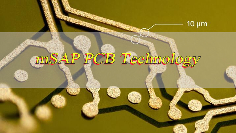
Are you troubled by traditional PCB fabrication limitations when developing smaller, denser, and faster electronic products? mSAP PCB Technology is the solution to these core pain points. Traditional etching cannot meet the demand for ultra-fine line widths and tight spacing, especially in the era of high-speed electronics where standard processes fall short. As a modified semi-additive process, mSAP achieves finer, more precise traces through selective copper plating, adapting well to advanced HDI and substrate-like PCBs. Read on to learn how mSAP can solve your PCB manufacturing challenges and unlock new design possibilities.
What is mSAP PCB Technology?
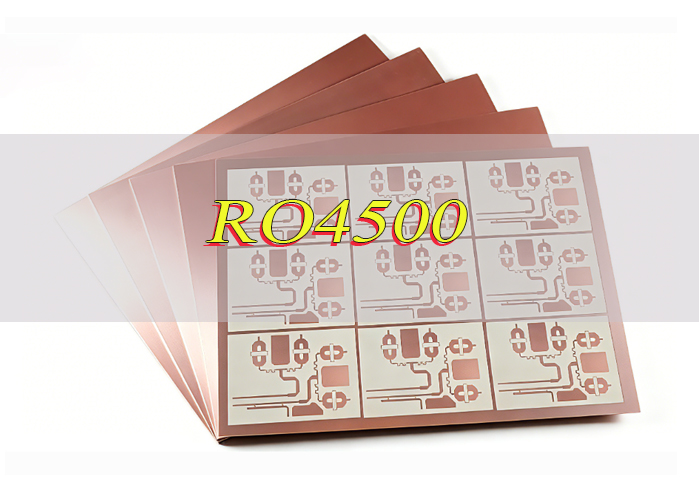
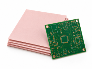
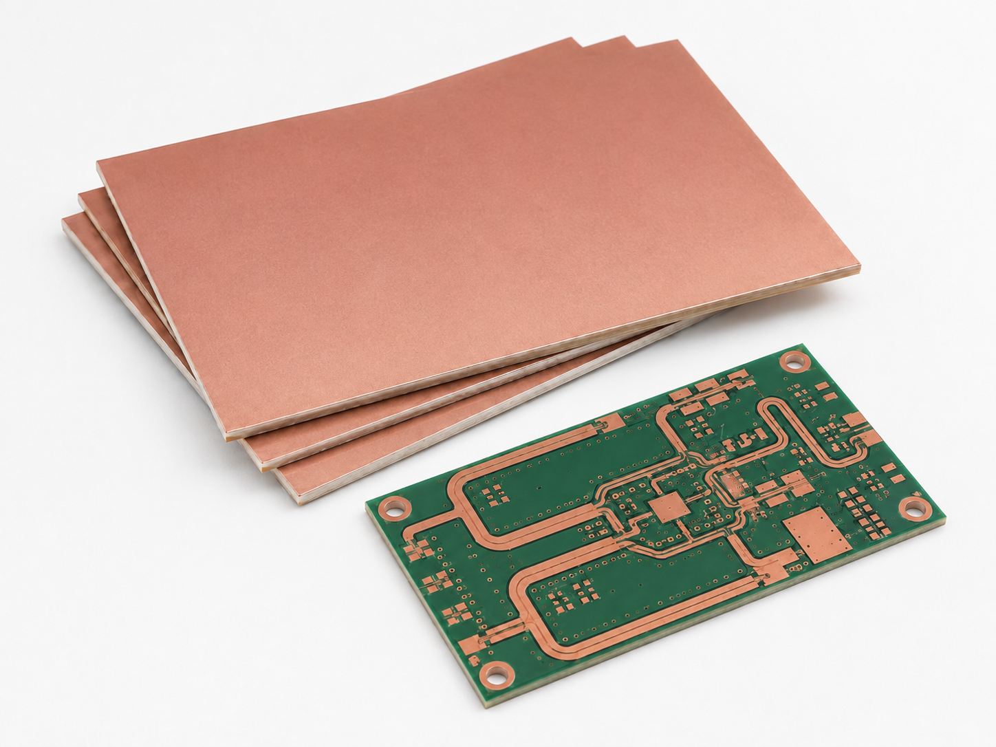
At its core, mSAP PCB technology officially the Modified Semi-Additive Process is a method for creating fine-line circuits in advanced PCB manufacturing. Unlike traditional subtractive processes, which start with a thick copper layer and etch away what’s not needed, mSAP begins with an extremely thin copper layer and selectively plates additional copper exactly where traces are required. This approach results in far finer, more precise circuit patterns, making it ideal for designs that demand small line widths, tight spacing, dense BGA escape routing, or shorter signal paths.
One of the pain points with traditional subtractive processes is that narrow traces are prone to copper undercut, which degrades sidewall quality. mSAP avoids this by focusing on building up copper rather than removing it, resulting in more vertical, tightly controlled trace profiles. From a technical standpoint, mSAP sits right between conventional HDI PCB fabrication and the more advanced SAP (Semi-Additive Process) or IC substrate processes it gives designers greater routing freedom while remaining far more practical for standard PCB production than full SAP.
What Are Advantages of mSAP PCB Technology?
mSAP really shines in advanced PCB manufacturing, especially for designs that need to pack a lot of routing into a small space. Here are its advantages:
- Finer Line and Space: Unlike conventional etching, mSAP supports much smaller line widths and spacing, letting you fit more traces into narrow routing channels.
- Higher Routing Density: With finer traces and tighter spacing, you can route more signals in the same board area either reducing the overall size of the PCB or adding more functionality without increasing its footprint.
- Better BGA Escape Routing: Fine-pitch BGA packages often require tight routing channels, and mSAP makes it easier to create more routing paths between pads critical for advanced processors, communication chips, and high-density modules.
- Cleaner Trace Geometry: Since mSAP relies on selective copper plating rather than heavy etching, trace sidewalls are more vertical, leading to more predictable electrical behavior.
- Improved Impedance Control: Stable trace geometry is key for controlled impedance designs, which are essential for high-speed digital signals, RF circuits, and communication boards.
- Shorter Signal Paths: Higher routing density means fewer long detours for signals, improving signal timing and overall layout efficiency.
- Support for Miniaturized Electronics: If you’re working on compact devices, wearables, 5G modules, or advanced HDI structures, mSAP is an excellent choice it’s built for small, high-performance PCBs.
- Better PCB Area Utilization: You can fit more functionality into the same board space, which is crucial for products where size, weight, and layout efficiency are top priorities.
What Are the Limitations of mSAP PCB Technology?
While mSAP is powerful, it’s not a one-size-fits-all solution. Here are its main limitations to keep in mind:
- Higher Manufacturing Cost: mSAP requires advanced imaging, plating, and inspection equipment, so it’s usually more expensive than standard subtractive PCB fabrication.
- Demanding Process Control: Fine-line production is sensitive to small variations even minor changes in exposure, plating, or flash etching can affect trace quality. This means you need stable equipment and precise process windows.
- Strict DFM Review: Before production, you’ll need to carefully review the layout, stackup, line/space, copper thickness, via structure, and impedance targets DFM (Design for Manufacturability) is even more critical with mSAP.
- Material Dependence: The substrate you use needs to support fine-line imaging, dimensional stability, and microvia reliability not all standard PCB materials are suitable for mSAP.
- Unnecessary for Standard Designs: For normal multilayer PCBs, power boards, or simple control boards, subtractive etching is still more efficient and cost-friendly. There’s no need to use mSAP if your design doesn’t require its fine-line capabilities.
What Are Applications of mSAP Technology?
mSAP is most useful in products where space is limited and circuit density is high. Here are some of its most common applications:
- Smartphones and Mobile Devices: These devices need compact boards with dense routing, fine-pitch components, and thin structures all areas where mSAP excels.
- Wearable Electronics: Wearables require small, lightweight, highly integrated PCBs, and mSAP helps fit more functions into a tiny space.
- 5G Communication Modules: 5G products need high-frequency performance, controlled impedance, compact layouts, and reliable signal paths mSAP delivers all of these.
- Advanced HDI PCBs: If your HDI design requires fine line/space, microvias, or high routing density, mSAP is the perfect match.
- Substrate-Like PCBs: These structures sit between conventional PCBs and IC substrates, and mSAP is well-suited to their unique requirements.
- Medical Electronics: Portable medical devices, monitoring equipment, and compact diagnostic modules often need reliable, dense interconnection mSAP fits the bill.
- Automotive Electronics: ADAS modules, sensors, control units, and high-speed automotive electronics often require fine routing and stable signal integrity mSAP delivers both.
- High-Speed Computing Modules: Advanced processors, memory modules, and high-speed interface boards benefit from mSAP’s shorter signal paths and tighter impedance control.
What Are Technical Parameters of mSAP PCB Technology?
The real value of mSAP lies in its tightly controlled parameters, all of which work together to enable its fine-line capabilities. Below is a detailed table of the technical parameters of mSAP PCB technology:
| Technical Parameter | Typical Range/Standard |
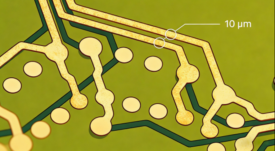
| Line Width | 20–60 μm (can reach 10–20 μm for advanced products) |
| Line Spacing | 20–60 μm (can reach 10–20 μm for advanced products) |
| Starting Copper Thickness | Extremely thin (typically a few micrometers) |
| Final Copper Thickness | Depends on design requirements, usually 10–50 μm |
| Trace Sidewall Shape | Clean, vertical (minimal undercut) |
| Registration Accuracy | High precision (typically ±5 μm or better) |
| Mask Alignment | Consistent with registration accuracy |
| Microvia Capability | Compatible with microvia formation (diameter down to 50 μm) |
| Impedance Control | Tight control (±5% tolerance typical) |
| Inspection & Testing | AOI, electrical testing, cross-section analysis |
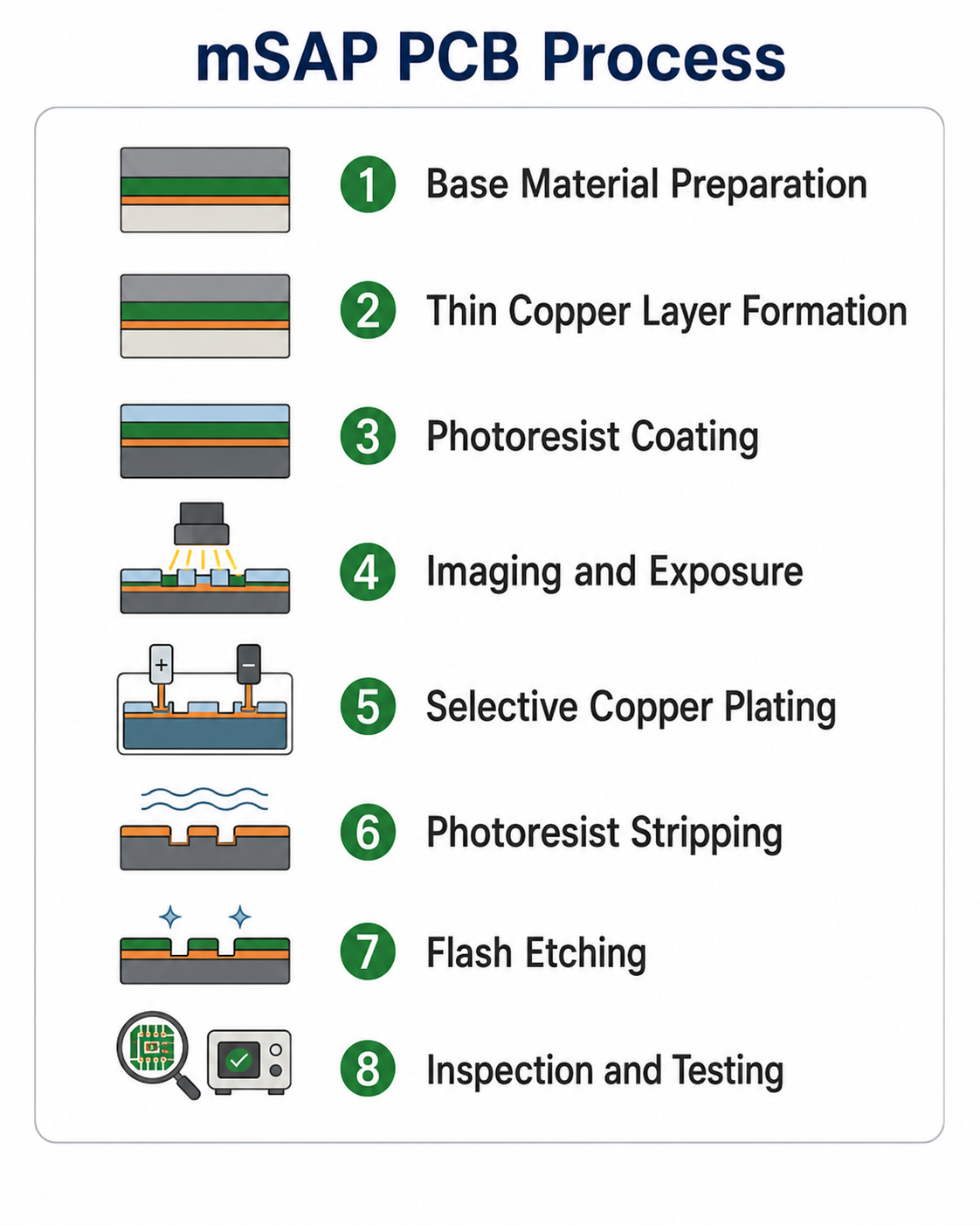
What is the Process of mSAP PCB?
The mSAP PCB process blends imaging, selective plating, and light etching, leaning more toward additive manufacturing but still including a controlled etching step to remove the thin seed copper layer. Here’s a step-by-step breakdown of how it typically works:
1. Base Material Preparation: We start with a dielectric material coated with an extremely thin copper layer one that’s suitable for fine-line imaging and microvia formation.
2. Surface Cleaning and Treatment: The copper surface is thoroughly cleaned and treated to improve adhesion, which is essential for ensuring consistent results in the subsequent plating and imaging steps.
3. Photoresist Coating: A layer of photoresist is applied to the copper surface; this layer will define exactly where copper will be plated and where it won’t.
4. Imaging and Exposure: The circuit pattern is transferred onto the photoresist via exposure, a step that requires precise mask positioning to avoid any pattern shifts even small misalignments can ruin fine-line circuits.
5. Development: The unwanted portions of the photoresist are removed, leaving open areas where copper will be plated.
6. Selective Copper Plating: Copper is plated only in the exposed circuit pattern areas this is the heart of mSAP’s fine-line advantage, as it allows for precise control over trace shape and size.
7. Photoresist Stripping: Any remaining photoresist is stripped away, leaving behind the newly plated copper traces.
8. Flash Etching: The thin seed copper layer between the traces is lightly etched away this is a gentle process, far easier to control than the heavy etching used in subtractive processes.
9. Inspection and Testing: AOI, electrical testing, and cross-section analysis are used to verify that the circuit meets all design requirements and quality standards.
To put it simply: subtractive etching forms traces by removing copper, while mSAP forms traces by adding copper selectively and only removing the thin seed layer resulting in cleaner, more precise circuits.
What is the Difference between SAP and mSAP?
While both SAP and mSAP fall under the semi-additive process family, they differ in several ways that make them suitable for different applications. Here’s a clear breakdown:
| Item | SAP | mSAP |
| Full Name | Semi-Additive Process | Modified Semi-Additive Process |
| Starting Copper Layer | Extremely thin seed copper | Thin copper layer (more PCB-production friendly) |
| Circuit Formation | Copper added to form traces (minimal starting copper) | Selective plating, then flash etching of seed layer |
| Line/Space Capability | Finer (closer to IC substrate-level) | Fine-line (for advanced HDI and substrate-like PCBs) |
| Main Application | IC substrates, ultra-fine circuits, advanced packaging | HDI PCB, compact electronics, substrate-like PCB |
| Process Complexity | Higher | High (but more adaptable to PCB manufacturing) |
| Cost | Generally higher | More practical for advanced PCB projects |
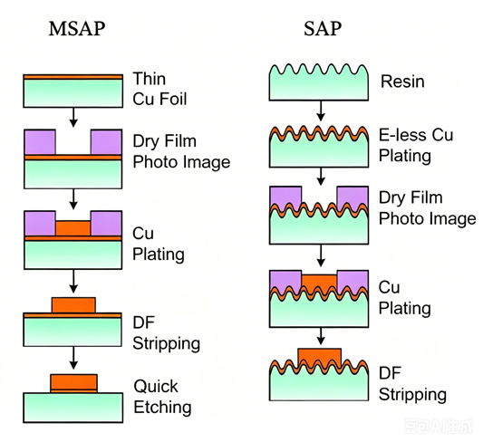
SAP is capable of extremely fine features, but it requires highly advanced process control. For most designs that need fine-line performance without the complexity of full SAP, mSAP is the preferred choice it’s far more aligned with standard PCB production methods while still delivering the necessary precision.
What is the Difference between Subtractive and mSAP?
The biggest difference between subtractive processes and mSAP boils down to how copper circuit patterns are created. Here’s a straightforward comparison to help you understand which is right for your project:
| Item | Subtractive Process | mSAP Process |
| Basic Principle | Removes unwanted copper | Adds copper where traces are needed |
| Starting Copper | Thicker copper foil | Very thin copper layer |
| Trace Formation | Mainly through etching | Mainly through selective plating |
| Fine-Line Control | Difficult for small traces | Ideal for fine-line patterns |
| Trace Sidewall | Prone to etching undercut | Cleaner, more vertical profile |
| Best Use | Standard PCB, common multilayer PCB, normal HDI | Advanced HDI, fine-line PCB, substrate-like PCB |
| Cost | More cost-effective for normal designs | Higher (but valuable for dense designs) |
Subtractive etching is still the go-to for standard PCBs it’s mature, reliable, and cost-effective. But when your design demands finer geometry, higher density, or tighter electrical control, mSAP is the clear upgrade.
Future Trends of mSAP PCB Technology
The future of mSAP is closely tied to the ongoing trends of miniaturization, high-speed electronics, and advanced packaging. Here’s what we can expect in the coming years:
- Growth of Substrate-Like PCB: As electronic products get thinner and more integrated, substrate-like PCBs will become more common and mSAP is perfectly positioned to support their fine-line and dense interconnection needs.
- More Demand from High-Speed and RF Designs: High-speed signals require tighter impedance control and more predictable trace geometry, and mSAP will become increasingly essential for these designs, especially as signal speeds continue to rise.
- Closer Connection Between PCB and Packaging: The line between PCB manufacturing and semiconductor packaging is getting blurrier, and mSAP (along with advanced HDI, SLP, and SAP) will play a key role in this integration.
- Improved Imaging and Registration Technology: Better direct imaging, exposure systems, and registration control will make mSAP more reliable, boosting yields and enabling even finer line/space capabilities.
- More Use in Compact Industrial and Medical Devices: mSAP will move beyond consumer electronics (like smartphones and wearables) and into more specialized, high-reliability applications, such as industrial sensors and medical devices.
- Stronger DFM Collaboration: Successful mSAP projects will require closer collaboration between product designers, PCB manufacturers, and assembly teams. Early DFM reviews will become even more important to reduce layout risk and ensure production success.
FAQs About mSAP PCB Technology
Q1: What is mSAP PCB Technology and how does it differ from traditional PCB manufacturing processes?
A1: mSAP (Modified Semi-Additive Process) is an advanced PCB manufacturing method designed to create fine-line circuits. Unlike traditional subtractive processes that etch away excess copper, mSAP starts with an extremely thin copper layer and selectively plates additional copper to form traces, then uses gentle flash etching to remove the remaining seed layer. This approach avoids copper undercut and achieves finer, more precise traces, making it ideal for high-density, miniaturized designs where traditional processes fall short.
Q2: What line width and spacing can mSAP PCB Technology typically achieve?
A2: The typical line width and spacing range for mSAP is 20–60 μm, and advanced mSAP processes can reach 10–20 μm. This is significantly finer than the capabilities of conventional subtractive etching, enabling higher routing density and more compact PCB designs for advanced electronic products.
Q3: How does mSAP compare to SAP (Semi-Additive Process) in terms of practicality and cost?
A3: Both are semi-additive processes, but SAP uses an extremely thin seed layer to achieve ultra-fine features (closer to IC substrate-level) with higher complexity and cost. mSAP is a modified, more practical version that balances performance and manufacturability, it supports fine-line routing but is more adaptable to standard PCB production, making it a more cost-effective choice for most advanced PCB projects.
Q5: What are the main limitations of mSAP PCB Technology that designers should consider?
A5: The primary limitations of mSAP include higher manufacturing costs (due to advanced equipment requirements), strict process control needs (small variations can affect trace quality), reliance on suitable substrate materials, and the need for rigorous DFM (Design for Manufacturability) reviews. Additionally, mSAP is unnecessary for standard PCB designs where traditional subtractive processes are more efficient and cost-friendly.
Q6: Does mSAP PCB Technology support impedance control, and why is this important?
A6: Yes, mSAP supports tight impedance control (typically ±5% tolerance) thanks to its ability to create clean, vertical trace sidewalls and precise trace geometry. This is critical for high-speed digital signals, RF circuits, and 5G modules, as stable impedance ensures reliable signal transmission and reduces interference.
Q7: What are mSAP PCB technology position masks and how do they affect the quality of mSAP PCBs?
A7: mSAP PCB technology position masks refer to the precise alignment and positioning of photoresist masks during the imaging and exposure stages of mSAP PCB manufacturing. They cover key aspects including mask positioning accuracy, photoresist alignment, exposure precision, and registration control. These masks directly affect mSAP PCB quality because even tiny deviations (a few micrometers) can lead to short circuits, inconsistent trace widths, or signal integrity issues that damage fine-line circuits.
Conclusion
mSAP PCB technology gives designers and manufacturers a practical way to build finer, denser, and more controlled circuit structures filling the gap where standard subtractive etching can no longer deliver. When comparing SAP vs mSAP, SAP offers finer capabilities but at the cost of greater complexity and expense. mSAP, on the other hand, strikes a balance between performance and practicality, making it ideal for advanced PCB production.
Subtractive processing still has its place for standard boards, but mSAP is invaluable for designs that demand fine-line HDI, compact electronics, or substrate-like PCBs. If your project requires high routing density, fine-pitch BGA escape, controlled impedance, or a smaller board size, mSAP is the technical advantage you need to bring your design to life.